Market Overview
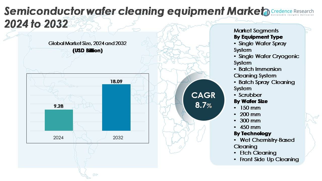
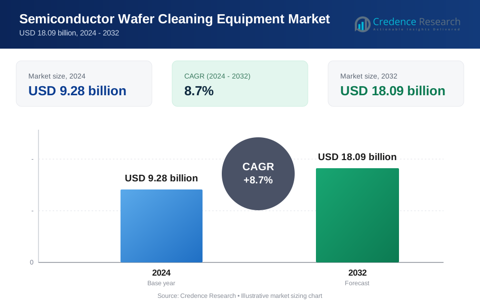
The semiconductor wafer cleaning equipment market was valued at USD 9.28 billion in 2024 and is projected to reach USD 18.09 billion by 2032, reflecting a CAGR of 8.7% during the forecast period.
| REPORT ATTRIBUTE | DETAILS |
|---|---|
| Historical Period | 2020-2023 |
| Base Year | 2024 |
| Forecast Period | 2025-2032 |
| Semiconductor Wafer Cleaning Equipment Market Size 2024 | USD 9.28 Billion |
| Semiconductor Wafer Cleaning Equipment Market, CAGR | 8.7% |
| Semiconductor Wafer Cleaning Equipment Market Size 2032 | USD 18.09 Billion |
The semiconductor wafer cleaning equipment market is shaped by a group of dominant global players, including Tokyo Electron, Lam Research, SCREEN Holdings, KLA Corporation, Hitachi High-Tech, Semes, Shibaura Mechatronics, Entegris, and Modutek, each contributing advanced wet processing, single-wafer cleaning, and contamination-control technologies. These companies compete through innovations in megasonic cleaning, precise chemical management, and low-damage processes essential for sub-5 nm nodes. Asia-Pacific leads the market with approximately 44% share, driven by extensive wafer fabrication in Taiwan, South Korea, Japan, and China. North America follows with around 28%, supported by major fab expansions in the U.S., while Europe accounts for about 17%, anchored by strong automotive and power semiconductor manufacturing.
Market Insights
- The semiconductor wafer cleaning equipment market was valued at USD 9.28 billion in 2024 and is projected to reach USD 18.09 billion by 2032, registering a CAGR of 8.7% during the forecast period.
- Strong market growth is driven by advanced-node migration below 7 nm, increased EUV adoption, and rising wafer starts across logic, memory, and specialty semiconductor production.
- Key trends include the shift toward low-damage cryogenic cleaning, wet chemistry optimization, AI-enabled process control, and increasing demand from power electronics, MEMS, and advanced packaging segments.
- The competitive landscape is dominated by Tokyo Electron, Lam Research, SCREEN Holdings, KLA, Hitachi High-Tech, Semes, Shibaura Mechatronics, Entegris, and Modutek, with single-wafer spray systems holding the largest segment share due to high precision requirements.
- Regionally, Asia-Pacific leads with ~44%, followed by North America at ~28% and Europe at ~17%, supported by major fab expansions, government incentives, and strong specialty semiconductor manufacturing.
Market Segmentation Analysis:
By Equipment Type
Single wafer spray systems dominate the semiconductor wafer cleaning equipment market, accounting for the largest share due to their ability to support advanced nodes below 10 nm, where particle removal efficiency and uniformity are critical. Their high throughput, precise chemical delivery, and compatibility with megasonic and ultrasonics enhance yield in logic and memory production. Batch immersion and batch spray systems remain relevant for legacy nodes and high-volume manufacturing, while cryogenic systems and scrubbers gain adoption in niche processes requiring minimal chemical use and reduced pattern damage. The shift toward smaller geometries continues to strengthen demand for single wafer spray platforms.
- For instance, SCREEN’s SU-3400 single-wafer cleaning system delivers up to 1,200 wafers per hour, a figure confirmed in SCREEN’s official product documentation. The platform also uses SCREEN’s proprietary Nanocontrol™ nozzle technology, which enables precise control of chemical flow and dispense positioning to protect advanced patterned wafers during high-throughput cleaning.
By Wafer Size
300 mm wafers represent the dominant wafer size segment, holding the highest market share as major foundries and IDMs operate on 300 mm production lines for high-performance computing, advanced memory, and automotive-grade semiconductors. Their larger surface area and higher die count per wafer drive extensive use of advanced cleaning tools that ensure defect-free substrates. While 200 mm wafers maintain steady demand from power electronics and analog segments, the industry’s long-term transition toward 450 mm remains slow due to high capital costs and limited ecosystem readiness. The ongoing expansion of 300 mm fabs globally reinforces the segment’s leadership.
For instance, a 300 mm wafer has a surface area of about 70,685 mm², while a 200 mm wafer has about 31,416 mm² a ratio of roughly 2.25×. This larger area supports far higher die output, which pushes fabs to adopt high-throughput wafer cleaning systems to maintain overall line efficiency.
By Technology
Wet chemistry–based cleaning leads the technology segment with the largest market share, driven by its proven efficiency in removing organic, metallic, and particulate contaminants using chemistries such as SC-1, SC-2, SPM, and dilute HF. Its adaptability to both single-wafer and batch systems makes it essential across advanced and mature nodes. Etch cleaning plays a significant role in oxide removal and surface preparation, particularly in FEOL processes, while front-side-up cleaning supports sensitive layers that require minimal pattern disruption. Continued scaling to sub-7 nm processes sustains the dominance of wet chemical cleaning solutions due to their high process reliability and selectivity.
Key Growth Drivers
Advanced Node Shrink and Rising Sensitivity to Sub-Micron Defects
Scaling toward 7 nm, 5 nm, and 3 nm nodes is one of the strongest growth drivers for semiconductor wafer cleaning equipment, as shrinking geometries significantly heighten sensitivity to nanoscale contaminants. Even particles below 20 nm can cause line bridging, contact failure, and device yield reduction, prompting fabs to adopt high-precision single-wafer cleaning systems with advanced megasonic, spray, and cryogenic technologies. More complex multilayer architectures in logic, 3D NAND, and DRAM require repeated cleaning steps often more than 80 per wafer increasing the total process count. As EUV lithography becomes mainstream, residues from photoresist materials, metal oxides, and post-etch byproducts demand new chemistries and low-damage cleaning processes. These requirements drive investment in tools with enhanced selectivity, improved chemical uniformity, and better control of pattern collapse, reinforcing the critical role of wafer cleaning equipment in sustaining device performance and yield.
- For instance, Lam Research reports that defectivity control at advanced nodes requires removal of particles as small as 3–5 nm during FEOL cleaning to prevent pattern collapse in high-aspect-ratio features.
Expansion of Global Fab Capacity and Front-End Manufacturing Investments
A surge in investments by leading foundries and IDMs is rapidly expanding the demand for advanced wafer cleaning solutions across both established and emerging semiconductor hubs. New fabrication facilities in the U.S., Europe, Taiwan, South Korea, Japan, and China are accelerating procurement of high-throughput cleaning systems to support increased wafer starts per month. Government-backed semiconductor incentive programs, reshoring strategies, and supply-chain resilience initiatives further intensify the pace of fab construction. Each new 300 mm fab requires large fleets of wet benches, single-wafer spray tools, megasonic units, and particle control systems, making cleaning equipment among the highest-volume process tools purchased. Additionally, specialty fabs producing power devices, MEMS, sensors, and automotive chips continue to upgrade to advanced cleaning platforms to meet quality and reliability standards. This robust global manufacturing expansion underpins sustained, long-term growth in equipment demand.
- For instance, TSMC’s Arizona Fab (Fab 21 Phase 1) is designed for an initial capacity of 20,000 300-mm wafers per month, requiring large fleets of single-wafer cleaning, megasonic, and wet-bench platforms to support leading-edge logic production.
Increasing Use of Complex Materials and 3D Device Architectures
The shift toward 3D structures including 3D NAND, gate-all-around FETs (GAAFETs), FinFETs, and advanced packaging significantly increases the need for specialized wafer cleaning technologies. Complex materials such as high-k dielectrics, cobalt, ruthenium, and advanced photoresists introduce new contamination challenges requiring precise chemical formulations and delicate removal processes. As vertical stacking increases surface complexity, residues become harder to access, demanding tools with enhanced chemical penetration, uniformity, and damage-free particle removal. Advanced cleaning equipment must also handle fragile low-k films and sensitive patterns without causing collapse or delamination. In heterogeneous integration and chiplet packaging, ultra-clean surfaces are essential for reliable bonding, TSV formation, and warpage-free assembly. These evolving material and architecture requirements drive adoption of specialized wet chemistry tools, cryogenic CO₂ cleaning, and ultra-low-pressure megasonic systems optimized for next-generation nodes.
Key Trends & Opportunities
Adoption of Cryogenic and Low-Damage Cleaning Processes
A major trend shaping the market is the growing adoption of cryogenic and low-damage cleaning technologies designed for delicate device structures. Cryogenic CO₂ cleaning, dry ice blasting, and reduced-pressure megasonic systems provide effective contamination removal while minimizing pattern collapse and surface erosion issues increasingly prevalent at sub-5 nm nodes. These innovations cater to advanced lithography and FEOL processes where low mechanical stress is essential. The opportunity lies in replacing traditional chemical-intensive methods with environmentally friendly alternatives that reduce consumption of sulfuric acid, ammonia, and HF-based solutions. As regulatory pressure strengthens and fabs pursue sustainability initiatives, cryogenic and low-chemical cleaning solutions gain traction. Equipment suppliers offering scalable, modular systems with hybrid cryogenic-wet cleaning capabilities stand to benefit significantly, especially in fabs transitioning toward greener, low-damage wafer cleaning ecosystems.
· For instance, CO₂ snow-jet cleaning systems documented in semiconductor process engineering studies generate particle velocities above 200 m/s, created as solid CO₂ expands through a supersonic nozzle. These high-speed particles provide enough kinetic energy to lift organic films and particles while remaining gentle on low-k and other fragile dielectric layers.
Increasing Automation, AI-Based Process Control, and Smart Fab Integration
The integration of AI-driven analytics, real-time process monitoring, and advanced automation is creating new opportunities across semiconductor cleaning operations. AI-enabled control systems optimize chemical dosing, bath life, spray parameters, and megasonic frequencies to maintain consistent results across wafer lots. Smart sensors, digital twins, and predictive maintenance models further support defect reduction and tool uptime optimization. As fabs transition toward highly automated “lights-out” manufacturing environments, wafer cleaning equipment must integrate seamlessly with factory automation platforms, AMHS systems, and advanced metrology. This trend enables productivity gains, lower operational costs, and significantly improved contamination control. Vendors offering AI-enhanced, fully automated single-wafer cleaning systems with remote diagnostics and closed-loop process feedback become increasingly valuable partners to semiconductor manufacturers.
- For instance, Lam Research’s Sense.i® platform captures more than 1,000 tool-state signals per second and generates over 1 terabyte of equipment data per day, enabling machine-learning models to identify process drifts before they affect wafer quality.
Growth of Specialty Segments Power Electronics, MEMS, and Advanced Packaging
Beyond leading-edge logic and memory, rising demand from specialty semiconductor segments presents strong opportunities for equipment suppliers. Power electronics based on SiC and GaN require robust cleaning processes to handle harder, more abrasive materials and high-temperature etch residues. MEMS fabrication depends heavily on precise wet etching and cleaning cycles to ensure sensor accuracy and microstructure integrity. Advanced packaging such as fan-out, CoWoS, and chiplets relies on ultra-clean surfaces for bonding, plating, and through-silicon via processing. These segments demand both high-throughput batch systems and advanced single-wafer tools tailored to diverse substrate materials. As electrification, IoT, and automotive electronics grow, specialized wafer cleaning becomes a key enabler of quality, reliability, and device performance.
Key Challenges
Complexity of Cleaning Fragile Structures at Sub-5 nm Nodes
As semiconductor nodes continue to shrink, cleaning equipment faces increasing difficulty in maintaining structural integrity while removing contaminants. Ultra-thin films, narrow trenches, and delicate 3D architectures are highly susceptible to pattern collapse, watermark formation, surface roughness, and dielectric erosion. Traditional high-power megasonic systems and aggressive chemistries can damage sensitive materials such as low-k dielectrics and high-aspect ratio structures. Ensuring uniform chemical distribution across complex geometries becomes another major challenge. Equipment manufacturers must continuously innovate low-pressure, low-damage solutions with precise control over particle energy, chemical exposure, and mechanical forces. Balancing cleaning effectiveness with structural protection remains one of the most persistent technical obstacles for tool suppliers.
High Capital Costs and Complexity of Integration in Advanced Fabs
Deploying advanced wafer cleaning tools involves significant capital investment, complex installation requirements, and lengthy qualification cycles. Fabs operating at 300 mm scale require large fleets of single-wafer tools, wet benches, dilution systems, and chemical recycling infrastructure, contributing to high total cost of ownership. Integrating new cleaning platforms with existing fab automation, metrology systems, and safety protocols adds further complications. The cost and complexity are particularly challenging for emerging fabs, small foundries, and specialty device manufacturers with limited budgets. Additionally, fluctuations in semiconductor demand cycles delay procurement and extend payback periods. Overcoming these economic and operational barriers requires equipment vendors to provide modular, scalable, and energy-efficient tools that reduce footprint, chemical usage, and long-term operating costs.
Regional Analysis
North America
North America holds around 28% of the global market, supported by strong investments in advanced semiconductor manufacturing driven by U.S. CHIPS Act incentives. Major foundries, including Intel, TSMC Arizona, and Micron, continue expanding 300 mm fabrication capacity, creating sustained demand for high-precision single-wafer and cryogenic cleaning tools. The region’s strong focus on leading-edge nodes below 5 nm intensifies requirements for advanced wet chemistry systems and low-damage megasonic equipment. Growth is further supported by increased adoption of AI, HPC, and automotive chips manufactured in U.S.-based fabs, reinforcing the region’s high technology intensity and equipment procurement momentum.
Europe
Europe accounts for approximately 17% of the market, driven by robust activity in specialty semiconductor production across Germany, France, the Netherlands, and Italy. Regional fabrication strengths include power electronics, MEMS, automotive semiconductors, and advanced packaging, all of which require specialized wafer cleaning solutions tailored to SiC, GaN, and sensor substrates. EU-backed semiconductor sovereignty programs and investments from players such as STMicroelectronics, Infineon, and GlobalFoundries expand regional equipment demand. Europe’s strong environmental regulations also accelerate the shift toward chemical-efficient wet benches and low-emission cleaning systems, positioning the region as a growing adopter of sustainable wafer cleaning technologies
Asia-Pacific
Asia-Pacific leads the global market with an estimated 44% share, driven by extensive wafer manufacturing in Taiwan, South Korea, Japan, and China. Major fabs including TSMC, Samsung, SK Hynix, UMC, SMIC, and Kioxia collectively account for the majority of global 300 mm wafer starts, requiring large-scale deployment of single-wafer spray tools, immersion benches, and megasonic systems. The region’s rapid transition to EUV-enabled nodes below 5 nm further boosts demand for ultra-pure, damage-free cleaning platforms. Expanding DRAM, NAND, logic, and foundry capacities, along with aggressive government subsidies, reinforce Asia-Pacific’s dominant role in the semiconductor wafer cleaning equipment ecosystem.
Latin America
Latin America holds around 6% of the market, primarily supported by growing demand for semiconductor packaging, testing, and electronics assembly operations in Mexico and Brazil. While the region does not host major advanced-node fabs, increasing investments in automotive electronics, consumer device assembly, and industrial automation support the adoption of cleaning tools for backend and specialty semiconductor applications. Multinational OEMs operating in Mexico’s electronics clusters drive procurement of batch cleaning systems, scrubbers, and wet benches. As regional manufacturing diversifies and supply chains shift closer to North America, Latin America’s demand for wafer cleaning equipment continues to gradually expand.
Middle East & Africa
The Middle East & Africa region accounts for an estimated 5% share, with growth emerging from government-led technology investments particularly in Israel and the UAE. Israel’s advanced semiconductor ecosystem, anchored by Intel and local design-to-manufacturing partners, drives demand for high-precision cleaning solutions in R&D and pilot-scale production. GCC countries are increasingly investing in microelectronics research parks and semiconductor supply-chain localization initiatives, generating opportunities for wet chemistry and contamination-control equipment. While large-scale wafer fabrication is still limited, rising interest in semiconductor diversification and strategic alliances supports gradual market penetration of cleaning technologies across the region.
Market Segmentations:
By Equipment Type
- Single Wafer Spray System
- Single Wafer Cryogenic System
- Batch Immersion Cleaning System
- Batch Spray Cleaning System
- Scrubber
By Wafer Size
- 150 mm
- 200 mm
- 300 mm
- 450 mm
By Technology
- Wet Chemistry-Based Cleaning
- Etch Cleaning
- Front Side Up Cleaning
By Geography
- North America
- U.S.
- Canada
- Mexico
- Europe
- Germany
- France
- U.K.
- Italy
- Spain
- Rest of Europe
- Asia Pacific
- China
- Japan
- India
- South Korea
- South-east Asia
- Rest of Asia Pacific
- Latin America
- Brazil
- Argentina
- Rest of Latin America
- Middle East & Africa
- GCC Countries
- South Africa
- Rest of the Middle East and Africa
Competitive Landscape
The competitive landscape of the semiconductor wafer cleaning equipment market is characterized by a concentrated group of global players specializing in advanced wet processing, single-wafer cleaning, and cryogenic technologies. Leading companies such as Tokyo Electron (TEL), SCREEN Semiconductor Solutions, Lam Research, Applied Materials, DNS, and SEMES dominate the high-end segment through continuous innovation in megasonic systems, chemical distribution control, and EUV-compatible cleaning platforms. These vendors compete on process precision, throughput, low-damage capability, and integration with smart fab automation. Mid-tier players, including Modutek, ACM Research, Entegris, and Ultron Systems, strengthen their presence by offering cost-effective wet benches, batch immersion tools, and modular systems tailored to specialty device manufacturing. Strategic partnerships with major foundries and IDMs are critical, enabling co-development of cleaning chemistries and process recipes. Ongoing investments in R&D, sustainability-driven chemical reduction, and AI-enabled process optimization further define competition, as suppliers aim to meet the demands of sub-5 nm nodes and increasingly complex 3D device architectures.
Key Player Analysis
- Shibaura Mechatronics Corporation (Japan)
- Modutek Corporation (US)
- Semes Co., Ltd. (South Korea)
- Entegris, Inc. (US)
- Tokyo Electron Limited (Japan)
- KLA Corporation (US)
- SCREEN Holdings Co., Ltd. (Japan)
- Hitachi High-Tech Corporation (Japan)
- Lam Research Corporation (US)
Recent Developments
- In September 2025, Entegris held a “Clean & Sustainable Fluid Delivery Technology Day,” highlighting its latest innovations and commitment to sustainable fluid-management systems across semiconductor manufacturing processes. While not a pure “wafer cleaning tool” launch, this reflects Entegris’ broader emphasis on contamination control, chemical delivery, and yield-enhancement integral complements to wafer cleaning workflows.
- In March 2024, Hitachi High-Tech introduced the LS9300AD a wafer-inspection tool that incorporates a new Differential Interference Contrast (DIC) optical system enabling detection of “low-aspect microscopic defects” on wafer surfaces and backsides. The system retains a rotating-stage wafer edge-grip and supports high throughput front/backside inspection, thereby improving defect detection sensitivity and yield control on unpatterned wafers.
Report Coverage
The research report offers an in-depth analysis based on Equipment type, Wafer size, Technology and Geography. It details leading market players, providing an overview of their business, product offerings, investments, revenue streams, and key applications. Additionally, the report includes insights into the competitive environment, SWOT analysis, current market trends, as well as the primary drivers and constraints. Furthermore, it discusses various factors that have driven market expansion in recent years. The report also explores market dynamics, regulatory scenarios, and technological advancements that are shaping the industry. It assesses the impact of external factors and global economic changes on market growth. Lastly, it provides strategic recommendations for new entrants and established companies to navigate the complexities of the market.
Future Outlook
- Demand for advanced wafer cleaning tools will accelerate as fabs transition to sub-5 nm and future 2 nm nodes.
- Adoption of EUV lithography will increase the need for ultra-low-damage cleaning processes and new chemistries.
- Single-wafer spray systems will gain stronger dominance due to higher precision and compatibility with advanced device architectures.
- Cryogenic CO₂ and dry-clean technologies will expand as fabs prioritize reduced chemical usage and sustainability.
- AI-driven process control and automation will become standard in next-generation cleaning platforms.
- Growth in 3D NAND, GAAFETs, and chiplet-based packaging will drive demand for more complex, selective cleaning solutions.
- Regional fab expansions in Asia-Pacific and North America will significantly boost long-term equipment procurement.
- Power electronics, MEMS, and advanced packaging fabs will increase investments in specialized cleaning tools.
- Vendors will focus on energy-efficient, resource-optimized tools to reduce total cost of ownership.
- Collaborative process development between equipment makers and leading foundries will intensify to meet next-generation cleaning challenges.
Request a Free Sample
Fill in your details and we'll send you a free sample report.
- Sample data tables & charts
- Research methodology
Market Dynamics
Advanced Node Shrink and Sub-Micron Defect Sensitivity
The migration to sub-7 nm, 5 nm, and 3 nm nodes increases sensitivity to nanoscale contaminants, requiring highly precise wafer cleaning equipment to prevent yield loss and device failure. This drives demand for advanced single-wafer cleaning systems with megasonic, spray, and cryogenic technologies.
Expansion of Global Fab Capacity
Significant investments in new fabrication facilities across the U.S., Asia, and Europe, supported by government incentives and reshoring strategies, are increasing the need for high-throughput wafer cleaning equipment to support rising wafer starts and advanced manufacturing processes.
Increasing Use of Complex Materials and 3D Architectures
The adoption of 3D NAND, GAAFETs, FinFETs, and advanced packaging introduces new contamination challenges, requiring specialized cleaning technologies and chemistries to handle fragile structures and complex material stacks without causing damage.
Adoption of Cryogenic and Low-Damage Cleaning Processes
As device structures become more delicate at advanced nodes, fabs are increasingly adopting cryogenic CO₂ and low-damage cleaning solutions to minimize pattern collapse and surface erosion, supporting both yield and sustainability goals.
Integration of AI-Based Process Control and Automation
The move toward smart, highly automated fabs is driving demand for wafer cleaning equipment with AI-enabled process control, real-time monitoring, and predictive maintenance, enabling higher productivity, lower operational costs, and improved contamination control.
Need a Custom Version of This Report?
Tailor the scope, geography, or segments to your exact requirements.
- Custom geography or segment scope
- Direct access to our analyst team
Frequently Asked Questions
What is the current market size for the Semiconductor Wafer Cleaning Equipment market, and what is its projected size in 2032?
At what Compound Annual Growth Rate is the Semiconductor Wafer Cleaning Equipment market projected to grow between 2024 and 2032?
Which Semiconductor Wafer Cleaning Equipment segment held the largest share in 2024?
What are the primary factors fueling the growth of the Semiconductor Wafer Cleaning Equipment market?
Who are the leading companies in the Semiconductor Wafer Cleaning Equipment market?
Which region commanded the largest share of the Semiconductor Wafer Cleaning Equipment market in 2024?
Table of Content
Chapter 1 Market Segmentation
- 1.1 Segmentation Framework
- 1.1.1 Product and Service Classification
- 1.1.2 Application and End-Use Classification
- 1.1.3 Technology and Solution Classification
- 1.1.4 Customer and Distribution Channel Classification
- 1.1.5 Geographic Segmentation
- 1.1.6 Market Segment Definitions and Boundaries
- 1.2 By Technology
- 1.2.1 Wet Chemistry-Based Cleaning
- 1.2.2 Etch Cleaning
- 1.2.3 Front Side Up Cleaning
- 1.3 By Wafer Size
- 1.3.1 150 mm
- 1.3.2 200 mm
- 1.3.3 300 mm
- 1.3.4 450 mm
- 1.4 By Equipment Type
- 1.4.1 Single Wafer Spray System
- 1.4.2 Single Wafer Cryogenic System
- 1.4.3 Batch Immersion Cleaning System
- 1.4.4 Batch Spray Cleaning System
- 1.4.5 Scrubber
Chapter 2 Introduction
- 2.1 Report Objectives and Scope
- 2.2 Product Definition and Industry Terminology
- 2.3 Market Inclusions and Exclusions
- 2.4 Research Process
- 2.4.1 Primary Research and Expert Interviews
- 2.4.2 Secondary Research and Source Review
- 2.4.3 Top-Down and Bottom-Up Estimation
- 2.4.4 Data Triangulation and Verification
- 2.5 Market Size Measurement Basis
- 2.5.1 2024: USD 9.28 billion → 2032: USD 18.09 billion
- 2.6 Historical and Forecast Reference Periods
- 2.6.1 Base Year: 2024
- 2.6.2 Forecast Period: 2024-2032
- 2.7 Research Assumptions and Limitations
Chapter 3 Executive Summary
- 3.1 Market Snapshot and Key Findings
- 3.2 Base-Year Market Size, 2024
- 3.3 Forecast Market Size, 2032
- 3.4 Revenue and Volume Growth Outlook
- 3.5 Key Demand and Supply Indicators
- 3.6 Leading Market Segments
- 3.7 Fastest-Growing Market Opportunities
- 3.8 Regional Performance Highlights
- 3.9 Technology and Industry Transformation
- 3.10 Competitive Landscape Summary
- 3.11 Analyst View and Strategic Implications
Chapter 4 Global Semiconductor Wafer Cleaning Equipment Market Trends and Developments
- 4.1 Historical Industry Development
- 4.2 Recent Market Trends and Developments
- 4.3 Demand and Customer Behavior Trends
- 4.4 Technology and Product Innovation
- 4.5 Artificial Intelligence, Automation and Digitalization
- 4.6 Local Manufacturing and Supply Chain Realignment
- 4.7 Industry Partnerships, Mergers and Acquisitions
- 4.8 Sustainability and Circular Economy Developments
- 4.9 Government and Private Sector Investment Trends
- 4.10 Emerging Business Models and Commercialization
- 4.11 Industry Developments and Announcements
Chapter 5 Global Semiconductor Wafer Cleaning Equipment Market Production, Supply and Demand Analysis
- 5.1 Demand Trend and Consumption Analysis
- 5.2 Demand Forecast, 2024-2032
- 5.3 Production and Output Trend
- 5.4 Production and Output Forecast, 2024-2032
- 5.5 Installed Capacity and Capacity Utilization
- 5.6 Company-Wise Production Plants and Statistics
- 5.6.1 Installed Production Capacity
- 5.6.2 Actual Production
- 5.6.3 Planned Capacity and Expansion Targets
- 5.7 Supply Chain Structure and Procurement Trends
- 5.8 Supply-Demand Gap and Bottlenecks
- 5.9 Import Dependence and Sourcing Structure
- 5.10 Contract Manufacturing and Outsourcing
- 5.11 Regional Supply and Demand Concentration
Chapter 6 Global Semiconductor Wafer Cleaning Equipment Market Pricing Analysis
- 6.1 Pricing Structure and Measurement
- 6.2 Historical Pricing Trends
- 6.3 Pricing Outlook, 2024-2032
- 6.4 Average Selling Price and Unit Economics
- 6.5 Pricing by Product and Market Segment
- 6.6 Geographic Pricing Differences
- 6.7 Key Input, Energy, Labor and Logistics Costs
- 6.8 Contract Pricing and Purchasing Models
- 6.9 Pricing Sensitivity and Competitive Positioning
- 6.10 Price, Margin and Profitability Implications
Chapter 7 Global Semiconductor Wafer Cleaning Equipment Market Dynamics
- 7.1 Market Growth Drivers
- 7.1.1 Demand-Side Drivers
- 7.1.2 Technology and Innovation Drivers
- 7.1.3 Infrastructure and Investment Drivers
- 7.1.4 Regulatory and Policy Drivers
- 7.2 Market Restraints
- 7.2.1 Cost and Affordability Constraints
- 7.2.2 Technology and Adoption Barriers
- 7.2.3 Supply Chain and Operational Constraints
- 7.3 Market Challenges
- 7.3.1 Competitive Pressure and Margin Erosion
- 7.3.2 Skills, Infrastructure and Implementation Gaps
- 7.4 Emerging Market Opportunities
- 7.5 Market Dynamics Impact and Time-Horizon Assessment
Chapter 8 Global Semiconductor Wafer Cleaning Equipment Value Chain Analysis
- 8.1 Industry Value Chain Overview
- 8.2 Upstream Suppliers and Critical Inputs
- 8.3 Technology and Component Providers
- 8.4 Manufacturing or Service Delivery
- 8.5 Distribution, Channel Partners and Integrators
- 8.6 Downstream Applications and End Users
- 8.7 Value Addition and Profit Pools
- 8.8 Vertical Integration and Outsourcing
- 8.9 Supplier Concentration and Risk
- 8.10 Supply Chain Localization and Resilience
Chapter 9 Global Semiconductor Wafer Cleaning Equipment Market Regulations and Policies
- 9.1 Relevant Laws, Standards and Compliance Frameworks
- 9.2 Product, Service, Safety and Quality Requirements
- 9.3 Government Policies, Incentives and Subsidies
- 9.4 Imports, Exports and Trade Barriers
- 9.5 Public Procurement and Local Content Requirements
- 9.6 Environmental and Sustainability Compliance
- 9.7 Upcoming Policy Changes and Market Implications
Chapter 10 Global Semiconductor Wafer Cleaning Equipment Market Hotspots and Opportunities
- 10.1 Market Opportunity Mapping and Growth Hotspots
- 10.2 High-Growth Applications and Customer Groups
- 10.3 Underserved Markets and White-Space Opportunities
- 10.4 Emerging Technology and Product Opportunities
- 10.5 New Capacity and Investment Hotspots
- 10.6 Market Entry and Expansion Opportunities
- 10.7 Distribution and Partnership Opportunities
- 10.8 Near-Term and Long-Term Commercial Potential
- 10.9 Opportunity Attractiveness and Execution Risks
Chapter 11 Global Semiconductor Wafer Cleaning Equipment Market Outlook, 2024-2032
- 11.1 Market Size and Analysis
- 11.1.1 Revenue (Market Measurement: 2024: USD 9.28 billion → 2032: USD 18.09 billion)
- 11.1.2 Market Volume and Quantity Sold
- 11.1.3 Historical Market Size
- 11.1.4 Base-Year Market Size, 2024
- 11.2 Market Forecast, 2024-2032
- 11.2.1 Revenue Forecast to 2032
- 11.2.2 Volume Forecast to 2032
- 11.2.3 CAGR and Year-on-Year Growth
- 11.2.4 Incremental Revenue Opportunity
- 11.3 Forecast Assumptions and Scenario Analysis
- 11.3.1 Base-Case Forecast
- 11.3.2 Optimistic and Conservative Scenarios
- 11.3.3 Technology, Pricing and Policy Sensitivities
- 11.4 Market Attractiveness and Growth Outlook
Chapter 12 Global Semiconductor Wafer Cleaning Equipment Market Segmentation and Outlook
- 12.1 Segmentation Summary and Market Shares, 2024
- 12.2 Largest and Fastest-Growing Segments
- 12.3 By Technology - Market Size and Forecast, 2024-2032
- 12.3.1 Segment Definition and Scope
- 12.3.2 Historical Market Size
- 12.3.3 Revenue Forecast, 2024-2032
- 12.3.4 Volume Forecast, 2024-2032
- 12.3.5 Base-Year Market Share, 2024
- 12.3.6 Segment CAGR and Growth Drivers
- 12.3.7 Subsegment Market Size and Forecast
- 12.3.7.1 Wet Chemistry-Based Cleaning
- 12.3.7.2 Etch Cleaning
- 12.3.7.3 Front Side Up Cleaning
- 12.3.8 Subsegment Pricing and Adoption Trends
- 12.3.9 Leading Suppliers and Competition
- 12.3.10 Regional Demand and Opportunities
- 12.4 By Wafer Size - Market Size and Forecast, 2024-2032
- 12.4.1 Segment Definition and Scope
- 12.4.2 Historical Market Size
- 12.4.3 Revenue Forecast, 2024-2032
- 12.4.4 Volume Forecast, 2024-2032
- 12.4.5 Base-Year Market Share, 2024
- 12.4.6 Segment CAGR and Growth Drivers
- 12.4.7 Subsegment Market Size and Forecast
- 12.4.7.1 150 mm
- 12.4.7.2 200 mm
- 12.4.7.3 300 mm
- 12.4.7.4 450 mm
- 12.4.8 Subsegment Pricing and Adoption Trends
- 12.4.9 Leading Suppliers and Competition
- 12.4.10 Regional Demand and Opportunities
- 12.5 By Equipment Type - Market Size and Forecast, 2024-2032
- 12.5.1 Segment Definition and Scope
- 12.5.2 Historical Market Size
- 12.5.3 Revenue Forecast, 2024-2032
- 12.5.4 Volume Forecast, 2024-2032
- 12.5.5 Base-Year Market Share, 2024
- 12.5.6 Segment CAGR and Growth Drivers
- 12.5.7 Subsegment Market Size and Forecast
- 12.5.7.1 Single Wafer Spray System
- 12.5.7.2 Single Wafer Cryogenic System
- 12.5.7.3 Batch Immersion Cleaning System
- 12.5.7.4 Batch Spray Cleaning System
- 12.5.7.5 Scrubber
- 12.5.8 Subsegment Pricing and Adoption Trends
- 12.5.9 Leading Suppliers and Competition
- 12.5.10 Regional Demand and Opportunities
- 12.6 Segment Growth Comparison
- 12.7 Segment Attractiveness and Priority Matrix
Chapter 13 Global Semiconductor Wafer Cleaning Equipment Geographic Market Outlook, 2024-2032
- 13.1 Regional Market Size and Share, 2024
- 13.2 Regional Market Forecast, 2024-2032
- 13.3 Regional Pricing, Production and Demand Differences
- 13.4 North America
- 13.4.1 United States
- 13.4.2 Canada
- 13.4.3 Mexico
- 13.5 Europe
- 13.5.1 Germany
- 13.5.2 France
- 13.5.3 Italy
- 13.5.4 United Kingdom
- 13.5.5 Spain
- 13.5.6 Poland
- 13.5.7 Russia
- 13.5.8 Netherlands
- 13.5.9 Belgium
- 13.5.10 Sweden
- 13.5.11 Denmark
- 13.5.12 Norway
- 13.5.13 Rest of Europe
- 13.6 Asia Pacific
- 13.6.1 China
- 13.6.2 India
- 13.6.3 Japan
- 13.6.4 South Korea
- 13.6.5 Thailand
- 13.6.6 Indonesia
- 13.6.7 Vietnam
- 13.6.8 Malaysia
- 13.6.9 Australia
- 13.6.10 Rest of Asia Pacific
- 13.7 Latin America
- 13.7.1 Brazil
- 13.7.2 Argentina
- 13.7.3 Colombia
- 13.7.4 Chile
- 13.7.5 Rest of Latin America
- 13.8 Middle East
- 13.8.1 Saudi Arabia
- 13.8.2 United Arab Emirates
- 13.8.3 Turkey
- 13.8.4 Israel
- 13.8.5 Iran
- 13.8.6 Rest of the Middle East
- 13.9 Africa
- 13.9.1 South Africa
- 13.9.2 Egypt
- 13.9.3 Nigeria
- 13.9.4 Morocco
- 13.9.5 Rest of Africa
- 13.10 Regional Investment, Policy and Supply Chain Differences
- 13.11 Regional Competitive Landscape
- 13.12 Geographic Growth Hotspots
Chapter 14 Global Semiconductor Wafer Cleaning Equipment Technology, Innovation and Sustainability Outlook
- 14.1 Technology Landscape and Maturity
- 14.2 Product, Process and Service Innovation
- 14.3 AI, Automation and Digital Tools in the Industry
- 14.4 Technology Adoption and Performance Benchmarking
- 14.5 Innovation Pipeline and R&D Investment
- 14.6 Patent and Intellectual Property Trends
- 14.7 Energy Efficiency and Resource Management
- 14.8 Sustainability, Recycling and Circularity
- 14.9 Technology Roadmap, 2024-2032
- 14.10 Risks of Obsolescence and Technology Substitution
Chapter 15 Global Semiconductor Wafer Cleaning Equipment Market Key Strategic Imperatives
- 15.1 Growth and Market Entry Priorities
- 15.2 High-Return Products and Segments
- 15.3 Pricing, Profitability and Cost Optimization
- 15.4 Technology Investment and Product Differentiation
- 15.5 Supply Chain Localization and Resilience
- 15.6 Distribution and Customer Acquisition
- 15.7 Partnership, Acquisition and Capacity Strategy
- 15.8 Regional Expansion Priorities
- 15.9 Short-, Medium- and Long-Term Actions
Chapter 16 Competition Outlook
- 16.1 Industry Competition Characteristics
- 16.2 Market Structure and Concentration
- 16.3 Market Share and Competitive Positioning, 2024
- 16.4 Company-Wise Revenue and Product Benchmarking
- 16.5 Production and Service Capacity Benchmarking
- 16.6 Technology, Pricing and Differentiation
- 16.7 Regional Footprint and Distribution Strength
- 16.8 Mergers, Acquisitions and Strategic Alliances
- 16.9 New Entrants and Competitive Threats
- 16.10 Porter's Five Forces and Industry Attractiveness
- 16.11 Competitive Outlook, 2024-2032
Chapter 17 Company Profiles
- 17.1 Company Coverage and Selection Criteria
- 17.2 Tokyo Electron Limited
- 17.2.1 Business Description
- 17.2.2 Company Ownership and Geographic Presence
- 17.2.3 Product and Service Portfolio
- 17.2.4 Manufacturing and Operating Footprint
- 17.2.5 Production Capacity and Expansion Plans
- 17.2.6 Financial Performance and Investment
- 17.2.7 Market Share and Competitive Position
- 17.2.8 Technology and Innovation Capabilities
- 17.2.9 Strategic Alliances or Partnerships
- 17.2.10 Recent Developments
- 17.2.11 Growth Strategy and Outlook
- 17.3 Lam Research Corporation
- 17.4 SCREEN Holdings Co., Ltd.
- 17.5 KLA Corporation
- 17.6 Hitachi High-Tech Corporation
- 17.7 Semes Co., Ltd.
- 17.8 Shibaura Mechatronics Corporation
- 17.9 Entegris, Inc.
- 17.10 Modutek Corporation
- 17.11 Applied Materials
- 17.12 Other Relevant Market Participants
Note: Every listed company is profiled on the structure shown under the first company. The company list is preliminary and may change based on research findings, market developments, data availability and client requirements.
Chapter 18 Disclaimer
- 18.1 Research and Forecast Disclaimer
- 18.2 Data Source and Estimation Limitations
Note: The depth of individual sections depends on data availability for this market. Volume, capacity, trade and other unit-based metrics are included where applicable.