
Infineon Makes First Power Devices on 300 mm Silicon Carbide Wafers in Volume Fab
Infineon Technologies AG said Nov. 9 that it has processed 300-millimeter silicon carbide wafers into working power semiconductor devices inside a full-scale production fab in Villach, Austria, a step the Munich-based chipmaker described as a world first. The company ran the wafers on manufacturing equipment already used for silicon, and a day later it reported record fourth-quarter revenue and set aside part of next year's capital budget for further silicon carbide capacity in Malaysia.
Key developments
- Infineon converted 300 mm silicon carbide (SiC) wafers into functional power devices in a full-scale fab environment in Villach, using existing silicon production tools.
- The company said a 300 mm wafer yields 2.3 times as many chips as a 200 mm wafer.
- Infineon will set 300 mm SiC technology and ramp timing with customers and partners while it continues its 200 mm SiC roadmap.
- The company showed that its Cold Split wafering process works with 300 mm SiC at its site in Dresden, Germany.
- On Nov. 10, Infineon reported fiscal 2026 revenue of 16.353 billion euros, up 12%, and planned fiscal 2027 investments of 3.0 billion to 3.5 billion euros, including SiC capacity expansion in Kulim, Malaysia.
How the technology works
Silicon carbide is a wide-bandgap semiconductor that handles higher voltages, temperatures and switching frequencies than conventional silicon. Those properties make it the material of choice for power conversion in electric vehicle traction inverters and on-board chargers, fast chargers, solar and storage systems, industrial drives and uninterruptible power supplies. Infineon also listed AI data centers, where SiC is used in solid-state transformers, circuit breakers and power supply units.
The material is hard to grow and hard to cut. Much of the industry's SiC output has come from 150 mm wafers, and producers have spent several years moving to 200 mm. Larger wafers spread fixed processing costs across more chips, which is why the jump to 300 mm matters. Infineon's approach relies on running SiC through tools built for 300 mm silicon, a format the company already uses at high volume in Villach and Dresden. Its Cold Split process, a laser-based technique, separates wafers from a SiC crystal boule with less material loss and much less processing time than wire sawing, so each crystal produces more wafers.
The wafer will go on public display at the electronica trade fair in Munich, which runs Nov. 10 to 13. Infineon did not disclose yields, device ratings, production volumes or a date for commercial output.
Industry implications
The announcement moves 300 mm SiC from substrate demonstrations toward device manufacturing. Wolfspeed said in January 2026 that it had produced a single-crystal 300 mm SiC wafer, and it described a path to future volume commercialization without giving a production date. Infineon's claim covers a later stage of the chain: finished, functional power devices processed in a production fab rather than a lab line.
For automakers and power electronics makers, the main question is cost. SiC devices still carry a premium over silicon insulated-gate bipolar transistors, and that premium has shaped how quickly EV makers adopt 800-volt platforms and SiC inverters. A wafer that carries 2.3 times as many chips, processed on depreciated silicon tooling, points to lower unit costs once yields mature. Infineon's own guidance on timing is cautious, however, and the company is pairing the 300 mm work with continued investment in 200 mm production.
The milestone also fits Infineon's push into data center power. Chief Executive Jochen Hanebeck said the milestone strengthens the company's position in power systems. He added that silicon, gallium nitride and now 300 mm SiC give Infineon a basis to scale manufacturing and grow profitably.
Competitive and supply chain implications
The SiC supply chain has been under strain. Chinese producers have added substrate capacity, EV demand in Europe and the United States has grown more slowly than planned, and several Western manufacturers have scaled back. Onsemi said Nov. 6 that it would not go ahead with an expansion of up to $2 billion at its SiC site in Rožnov pod Radhoštěm, Czech Republic. Against that backdrop, Infineon is betting that process scale and existing silicon tooling can protect margins.
Using silicon equipment also reduces reliance on specialized SiC tool sets and could ease the capital burden of new capacity. Wafer supply remains a constraint. Infineon sources substrates from several suppliers, including Wolfspeed, and is developing its own wafering capability with Cold Split. Larger-diameter substrates in commercial quantities will determine how fast any 300 mm ramp can proceed, which gives crystal growers a central role in the next phase.
Rivals including STMicroelectronics, onsemi, Rohm, Bosch and Chinese device makers have been moving production to 200 mm wafers. A credible 300 mm route could push them to revisit their own technology plans.
Regional implications
Europe gains the most immediate benefit. Villach, where the wafers were processed, is also the site of Infineon's planned high-volume gallium nitride fab on 300 mm wafers, an investment of about 1.1 billion euros announced Oct. 27. Dresden, where the Cold Split feasibility work took place, hosts Infineon's newest silicon fab, which the company is ramping in fiscal 2027.
Malaysia remains the center of Infineon's SiC volume plans. The company opened the first phase of its Kulim 3 fab in August 2024, a 2 billion euro investment that it described as the world's largest 200 mm SiC power fab, with about 5 billion euros in new design wins and about 1 billion euros in customer prepayments at the time. Infineon's results release named SiC capacity expansion in Kulim as one of its main investment projects for fiscal 2027.
Credence Research analysis
Infineon's milestone is significant mainly for what it suggests about cost structure. By showing SiC devices can be made on silicon-class 300 mm tools, the company is signaling that future SiC capacity may be added at existing silicon fabs rather than in dedicated plants. That would let Infineon shift tools and cleanroom space between silicon, gallium nitride and SiC as demand moves, an advantage in a cycle where EV-related SiC demand has been uneven and data center power demand has risen fast.
The gap between a working device and volume output is still wide. Infineon has not given yields or a ramp date, and 300 mm substrates are not yet available in commercial quantities. The near-term effect is therefore on customer negotiations and competitor planning more than on supply. The timing, alongside a record quarter and a capital budget of up to 3.5 billion euros, shows that Infineon is willing to keep investing in power semiconductors while peers retreat.
What comes next
- Public showing of the 300 mm SiC wafer at electronica in Munich, Nov. 10 to 13, 2026.
- Talks with customers and partners to set 300 mm SiC technology specifications and ramp timing.
- Continued execution of Infineon's 200 mm SiC roadmap, including capacity expansion in Kulim during fiscal 2027.
- Progress on the 1.1 billion euro, 300 mm gallium nitride fab in Villach and the Dresden fab ramp.
- Further disclosures from Wolfspeed and other substrate makers on commercial supply of 300 mm SiC wafers.
Sources
- Infineon: world's first 300-millimeter power silicon carbide wafer (Nov. 9, 2026)
- Infineon fiscal 2026 results release via EQS (Nov. 10, 2026)
- Wolfspeed: 300mm silicon carbide technology breakthrough (Jan. 13, 2026)
- Power Electronics News: Infineon inaugurates 200 mm SiC fab in Kulim (Aug. 2024)
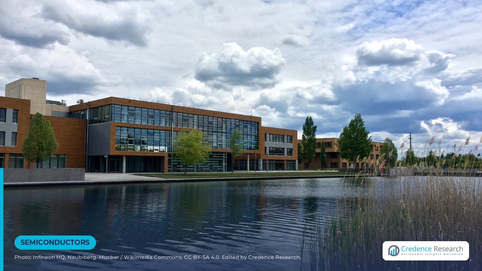
Image: Campeon headquarters of Infineon Technologies AG in Neubiberg near Munich, by Mucber via Wikimedia Commons, CC BY-SA 4.0. Cropped and edited by Credence Research.

About the Author

Senior News Editor at Credence Research Inc