
Infineon to Invest 1.1 Billion Euros in First High-Volume 300mm GaN Power Chip Fab in Villach
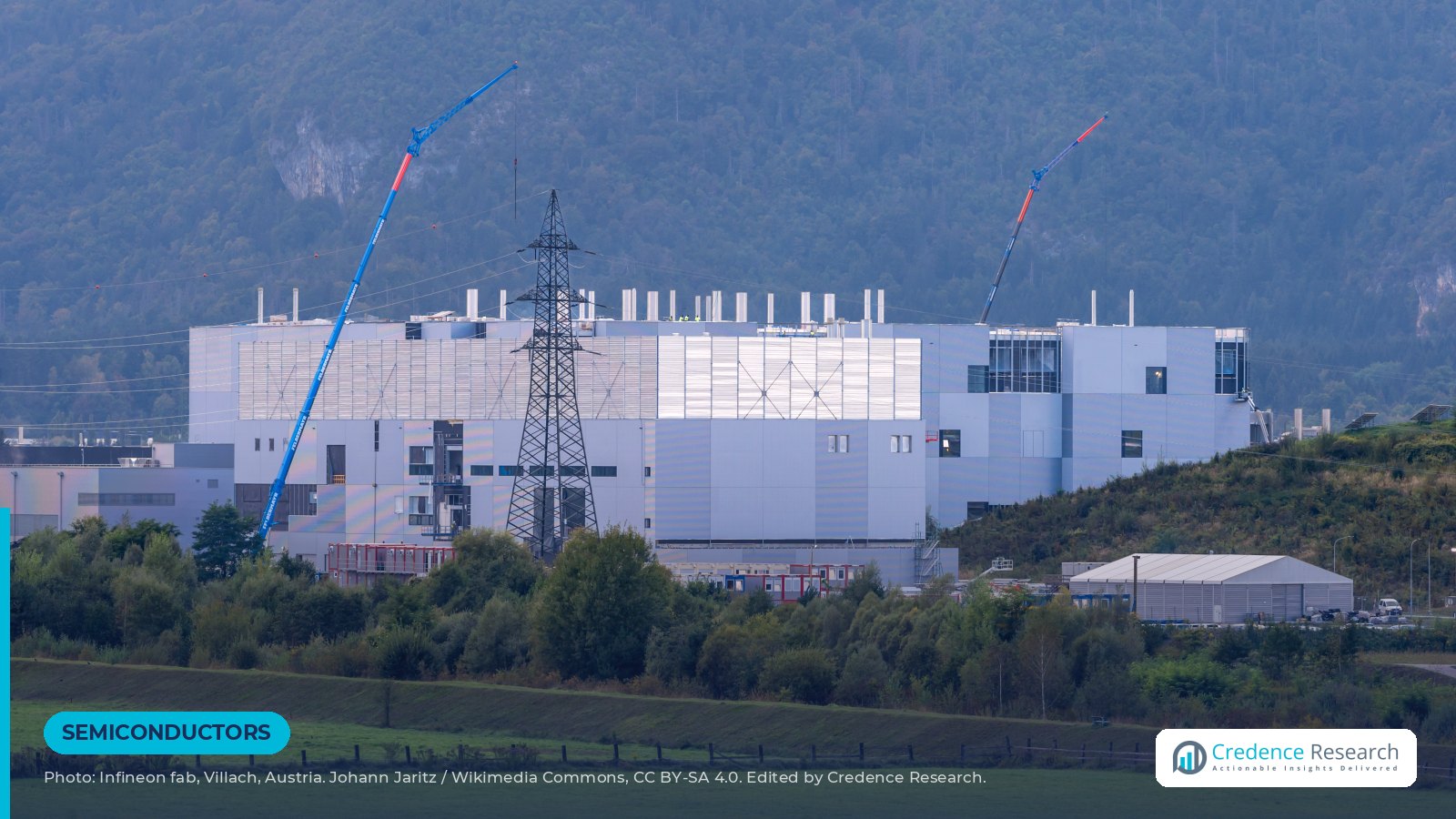
Infineon Technologies said on Oct. 27, 2026, that it will invest about 1.1 billion euros in its Villach, Austria, site to build what it describes as the world's first high-volume manufacturing facility for gallium nitride power semiconductors on 300-millimeter wafers. The Munich-based chipmaker plans to install the new production inside existing cleanrooms in Villach, with output scheduled to start by the end of 2027 and spending running through 2034.
Key developments
- Infineon will invest about 1.1 billion euros by 2034 in existing and upgraded cleanroom infrastructure at Villach for gallium nitride (GaN) power chips made on 300-millimeter wafers.
- Production is scheduled to begin by the end of 2027, and the company said capacity will be ramped in line with demand.
- The European Commission has approved 319 million euros in state aid for the project under the European Chips Act. Austria's Federal Ministry for Economic Affairs, Energy and Tourism still has to issue a formal funding commitment, subject to location-specific criteria.
- Infineon said a 300-millimeter GaN wafer yields about 2.3 times as many chips as a 200-millimeter wafer.
- Infineon Austria employs about 5,800 people, about 4,800 of them in Villach. The company did not say how many new jobs the facility will add.
How the technology works
Gallium nitride is a wide-bandgap semiconductor material. In power electronics it switches faster and converts electricity with lower losses than conventional silicon transistors, which means less waste heat and smaller, lighter power supplies, chargers and inverters. Infineon named AI data centers, energy infrastructure, e-mobility, robotics and consumer electronics as the main applications for the chips it will make in Villach.
Most GaN power devices today are built on 200-millimeter or smaller wafers. Moving to 300 millimeters lets a fab produce far more chips per wafer pass and use the same large-diameter tools that silicon fabs already run. Infineon said it processed the world's first 300-millimeter GaN power wafers two years ago and is now transferring that process into volume production for customers. The company has also said it is working with NVIDIA on GaN-based power conversion for 800-volt direct-current AI data center architectures, one of the fastest-growing uses for high-efficiency power chips.
Villach is Infineon's long-standing center for power semiconductors. The company opened a 300-millimeter power electronics fab at the site in 2021, and the GaN project will reuse cleanroom space there rather than requiring a new building, which Infineon said keeps the expansion cost-efficient.
Industry implications
The announcement moves GaN power electronics a step closer to the cost and volume profile of silicon. Data center operators are under pressure to cut conversion losses as rack power densities climb, and automakers and industrial equipment makers are looking for smaller, cooler power stages. A larger wafer format improves the economics of each device, which could widen GaN adoption beyond chargers and niche high-end applications into server power supplies, onboard chargers and motor drives.
The timing also matters for buyers who plan multiyear product cycles. A firm production start date at the end of 2027 gives power supply designers and data center hardware suppliers a qualification window, and Infineon's statement that capacity will follow demand signals a phased rather than all-at-once build.
Competitive and supply chain implications
Infineon operates as an integrated device manufacturer, designing and fabricating its own chips, and it strengthened its GaN position when it acquired Canada's GaN Systems in 2023. Owning 300-millimeter GaN capacity gives the company control over supply at a time when the foundry route is narrowing. TrendForce has reported that TSMC plans to exit GaN production by July 2027, which leaves fabless GaN designers that relied on it lining up other foundries.
For rivals that build GaN on smaller wafers, a high-volume 300-millimeter line raises the bar on cost per chip. It also keeps more of the power semiconductor supply chain inside Europe, where Infineon already makes silicon and silicon carbide power devices. Equipment and materials suppliers that serve 300-millimeter tools and epitaxy could see follow-on orders as the line is built out through 2034.
Regional implications
Austrian officials framed the project as a national industrial milestone. Federal Chancellor Christian Stocker called it one of the largest single investments in the history of Austria's high-tech industry. Economy Minister Wolfgang Hattmannsdorfer noted that Europe accounts for only about 10% of global chip production and said Austria intends to support the project with up to 319 million euros, tied to clear funding criteria.
The investment adds to a series of European Chips Act-backed fabs, including TSMC's joint venture plant in Dresden and Infineon's own expansion in that city. Sabine Herlitschka, chief executive of Infineon Technologies Austria, described the Villach project as a flagship for moving research into industrial production, with ties to local universities, research institutes and start-ups in the Carinthia region.
Credence Research analysis
The most significant element of the announcement is the combination of wafer size and timing. GaN has long been held back less by performance than by cost and supply concentration. By placing 300-millimeter GaN into an existing power fab with a production date of late 2027, Infineon is positioning itself to absorb demand from data center power and electrification customers just as one of the largest GaN foundry sources is reported to be winding down. The use of existing cleanrooms also lowers execution risk compared with greenfield construction.
Several conditions still apply. The Austrian funding commitment is not yet final, the company has not disclosed initial capacity or headcount additions, and the ramp will be paced by demand. Infineon shares had fallen about 40% since mid-June before the announcement, according to Reuters, suggesting investors will watch how the spending fits within the company's broader capital plans. Customer qualification results and design wins in data center power supplies will be the clearest early signals of whether the investment pays off.
What comes next
- Formal funding commitment from Austria's Federal Ministry for Economic Affairs, Energy and Tourism.
- Equipment installation and transfer of the 300-millimeter GaN process into existing Villach cleanrooms ahead of the production start.
- Start of 300-millimeter GaN volume production by the end of 2027.
- Customer qualification and design wins in AI data center power, e-mobility and industrial systems.
- Phased capacity expansion and continued investment at the site through 2034.
Sources
- Infineon Technologies press release, Oct. 27, 2026 (via PCIM News)
- Semiconductor Today, Oct. 27, 2026
- Reuters report via Global Banking and Finance Review, Oct. 27, 2026
- TrendForce: TSMC to exit GaN production by July 2027
Image: Infineon's 300-millimeter power semiconductor fab under construction in Villach-Auen, Austria, in 2020, by Johann Jaritz via Wikimedia Commons, CC BY-SA 4.0. Cropped and edited by Credence Research.

About the Author

Senior News Editor at Credence Research Inc