
Samsung Breaks Ground on Onyang HBM Packaging Fab as Chungcheong Mega Project Starts
Samsung Electronics broke ground on Nov. 12 on a dedicated high-bandwidth memory (HBM) packaging fab at its Onyang Campus in Asan, South Chungcheong Province, marking the formal start of a Samsung group investment plan for South Korea's Chungcheong region. President Lee Jae-myung and Samsung Electronics Executive Chairman Lee Jae-yong attended the ceremony, which South Korea's Ministry of Industry and Trade used to unveil a comprehensive government support package for what it calls the Chungcheong Mega Project.
Key developments
- The Ministry of Industry and Trade said Samsung Electronics will invest 6 trillion won in a new fab dedicated to HBM packaging at Onyang Campus, one of three Samsung projects that started construction on Nov. 12.
- The Korea Times reported that Samsung plans a total of 46 trillion won at Onyang, with 6 trillion won for construction and 40 trillion won for equipment installed in stages, and that the new fifth line targets operation in June 2028, a year ahead of the original schedule.
- The ministry listed two affiliate projects alongside Onyang: an 8 trillion won Samsung Electro-Mechanics investment in semiconductor package substrate lines for GPUs and CPUs in Sejong, and a 67 trillion won Samsung Display investment in an 8.6-generation IT panel line in Cheonan and Asan.
- Korean media reported that Samsung raised its group-wide Chungcheong commitment to 144 trillion won, up from about 140 trillion won announced on July 2.
- The government pledged 1.9 trillion won through 2030 for 14 advanced-industry infrastructure facilities, 1.5 trillion won to upgrade industrial complexes and training for 10,000 advanced-industry workers a year in the region.
Why HBM packaging matters
High-bandwidth memory stacks multiple DRAM dies vertically and connects them through thousands of interconnects, so that AI accelerators can move data far faster than conventional memory allows. The stacking, bonding and testing steps happen in back-end packaging plants, and those steps have become a production bottleneck as each new HBM generation adds layers and input/output pins. Samsung's HBM4, which it said in February 2026 had entered mass production and commercial shipment, doubles data I/Os to 2,048 pins and supports stacks of up to 16 layers.
Onyang has historically handled conventional chip assembly and testing. According to the Korea Times, the new line will add about 31,000 square meters of cleanroom across three floors and lift the campus floor area from about 270,000 to about 420,000 square meters. Samsung first outlined five HBM fab lines for Onyang in its July 2 plan, which also covered HBM equipment upgrades in Cheonan, a next-generation battery verification line for Samsung SDI in Cheonan and expanded AI server substrate capacity for Samsung Electro-Mechanics in Sejong. The company set a target of 250,000 jobs for the overall regional plan.
Industry implications
The acceleration signals that Samsung sees packaging, rather than wafer output alone, as the constraint on HBM supply. The Korea Times reported that Samsung said at its third-quarter earnings that it had completed HBM supply volume negotiations for 2027 but that customers had requested additional volume, and that the company expects supply shortages to persist through 2028. Pulling the Onyang start forward by a year is the clearest operational response to that position.
Executive Chairman Lee told the ceremony that the site would become a leading hub for advanced HBM, which he described as the heart of AI chips. The Seoul Economic Daily reported that Lee told President Lee that Samsung would mass-produce HBM4E, its next generation, at the new line. For AI accelerator designers and hyperscale cloud operators, a dedicated packaging fab with a firm 2028 date offers a planning anchor for memory availability as next-generation GPU and custom accelerator platforms ramp.
Competitive and supply chain implications
The project intensifies a capacity race in advanced memory packaging. SK hynix broke ground in August 2026 on an advanced packaging plant in West Lafayette, Indiana, with expected spending of more than $4 billion, a cleanroom due by October 2028 and mass production of next-generation HBM planned for the second half of 2029, according to Evertiq. Samsung's Onyang timetable would put its new domestic capacity online ahead of that U.S. plant.
The supply chain effects extend well beyond Samsung. The 40 trillion won equipment budget reported for Onyang points to sustained orders for thermocompression and hybrid bonding tools, wafer-level test equipment and inspection systems. Samsung Electro-Mechanics' Sejong substrate lines address another tight input for AI servers. The ministry also earmarked 48.7 billion won through 2028 for 17 joint R&D projects between parts and materials suppliers and anchor companies, aimed at deepening the domestic supplier base around the new fabs.
Regional implications
The Ministry of Industry and Trade said the Chungcheong plan covers eight anchor companies and 10 projects, with six starting construction in 2026, two in 2027 and two in 2028 or 2029. Alongside the infrastructure and industrial complex funding, the government plans four advanced national industrial complexes, four specialized parts and materials complexes and three advanced-industry specialized complexes, plus faster permitting, subsidies, tax credits and help with power and water supply. Industry Minister Kim Jung-kwan described Chungcheong as a central hub for semiconductors, displays, batteries and biotechnology.
The Korea Times reported that the Onyang fab is expected to create about 700 jobs and that construction will employ an average of 3,400 workers a day. It also reported that South Chungcheong Province and Asan City cut permit review times to about one-third of the usual period. The talent program will run through a new college at Chungnam National University, specialized universities, academies and bootcamps.
Credence Research analysis
The Onyang groundbreaking shows how the bottleneck in AI memory has shifted downstream. Front-end DRAM capacity still matters, but HBM output now depends on how quickly makers can stack, bond and test 12- and 16-high dies at acceptable yields. By dedicating a fab to packaging and committing most of the reported budget to equipment, Samsung is treating back-end process control as a competitive capability in its own right, rather than a cost center. The June 2028 target also aligns the plant with the expected transition to HBM4E, giving Samsung a facility designed around that generation from the start.
The government's role is equally significant. Bundling permits, utilities, training and supplier R&D into one package reduces execution risk for a project of this size and keeps advanced packaging, along with its skilled workforce, inside South Korea even as rivals add U.S. capacity. The main risks are execution and timing: equipment lead times, bonding yields at higher stack counts and the pace of AI infrastructure spending will determine whether a 2028 start converts into competitive supply.
What comes next
- Construction of Onyang Line 5, targeting operation in June 2028, as reported by the Korea Times.
- Staged installation of packaging and test equipment at Onyang under the reported 40 trillion won equipment budget.
- Samsung Electro-Mechanics' Sejong substrate lines, which the Korea Times reported are set for mass production in September 2028.
- Construction starts on the remaining Chungcheong anchor projects under the ministry's schedule of six starts in 2026, two in 2027 and two in 2028 or 2029.
- Rollout of the government's infrastructure, industrial complex and talent programs through 2030.
Sources
- Ministry of Industry and Trade via Korea.kr: Chungcheong Mega Project groundbreaking and support plan (Korean)
- Samsung Newsroom: Samsung plans 140 trillion won investment in Chungcheong (Korean)
- The Korea Times: Samsung Electronics breaks ground on new HBM packaging facility in Asan
- Evertiq: SK hynix breaks ground on packaging facility in Indiana
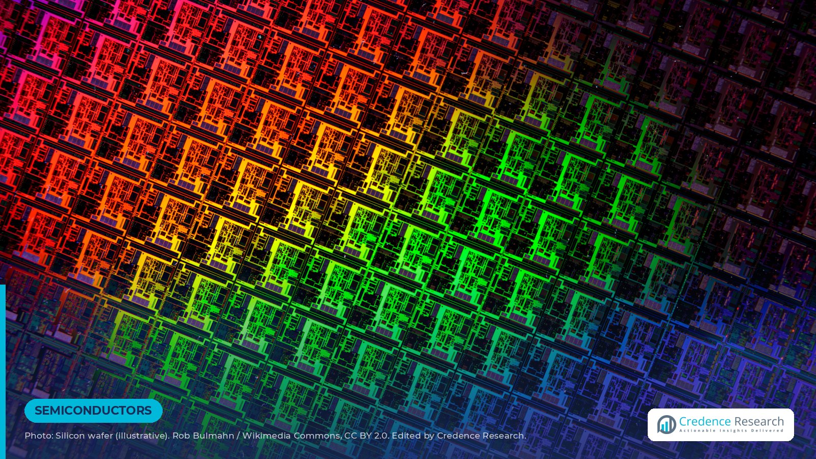
Image: Silicon wafer (illustrative), by Rob Bulmahn via Wikimedia Commons, CC BY 2.0. Cropped and edited by Credence Research.

About the Author

Senior News Editor at Credence Research Inc