Market Overview
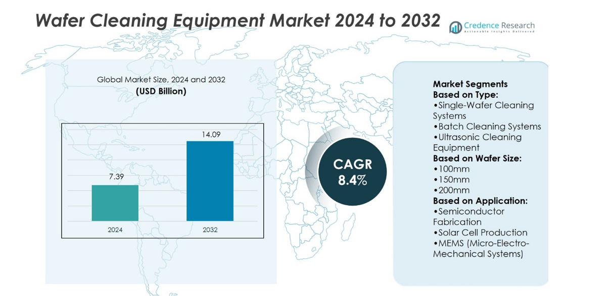
Wafer Cleaning Equipment Market size was valued at USD 7.39 billion in 2024 and is anticipated to reach USD 14.09 billion by 2032, at a CAGR of 8.4% during the forecast period.
| REPORT ATTRIBUTE | DETAILS |
|---|---|
| Historical Period | 2020-2023 |
| Base Year | 2024 |
| Forecast Period | 2025-2032 |
| Wafer Cleaning Equipment Market Size 2024 | USD 7.39 billion |
| Wafer Cleaning Equipment Market, CAGR | 8.4% |
| Wafer Cleaning Equipment Market Size 2032 | USD 14.09 billion |
The Wafer Cleaning Equipment Market grows through strong demand for advanced semiconductor devices, stricter contamination control, and expansion of global fabrication facilities. It benefits from the shift toward single-wafer cleaning systems that deliver higher precision and support advanced nodes below 10nm. Automation, AI-driven monitoring, and eco-efficient designs enhance equipment efficiency and reduce operational costs. The rise of 300mm and upcoming 450mm wafers drives innovation in cleaning technologies. Growing applications in semiconductor fabrication, solar cells, MEMS, and LEDs strengthen adoption. Sustainability goals and green manufacturing practices further shape trends, positioning cleaning equipment as a critical enabler of next-generation chip production.
The Wafer Cleaning Equipment Market shows strong geographical concentration in Asia-Pacific, holding the largest share due to extensive semiconductor production in China, Taiwan, South Korea, and Japan. North America and Europe follow with advanced fabs, research institutions, and strong adoption of eco-efficient technologies, while Latin America and the Middle East & Africa remain emerging markets. Key players driving the market include Applied Materials, Tokyo Electron, Lam Research, Screen Holdings, Entegris, Suss Microtec, PVA Tepla, Shibaura Mechatronics, and Modutek.com.
Market Insights
- Wafer Cleaning Equipment Market size was USD 7.39 billion in 2024 and will reach USD 14.09 billion by 2032, growing at a CAGR of 8.4%.
- Strong demand for advanced semiconductor devices and strict contamination control drives steady market expansion.
- Single-wafer cleaning systems gain preference for advanced nodes below 10nm due to higher precision.
- Automation, AI-based monitoring, and eco-efficient technologies improve productivity and reduce operational costs.
- High equipment costs and technical complexity remain restraints for small and mid-sized fabs.
- Asia-Pacific leads the market with the largest share, followed by North America and Europe, while Latin America and Middle East & Africa emerge gradually.
- Key players strengthen competition through innovation, partnerships, and eco-friendly product portfolios.
Market Drivers
Rising Demand for Advanced Semiconductor Devices Driving Cleaning Equipment Adoption
The Wafer Cleaning Equipment Market expands with the increasing complexity of semiconductor devices. Advanced chips for AI, 5G, and IoT require ultra-clean surfaces to ensure efficiency. Manufacturers invest in cleaning systems that handle nanoscale contamination without damaging delicate structures. It supports consistent yields and stable production for high-performance devices. Stringent quality standards push suppliers to deliver precision cleaning technologies. This demand strengthens equipment adoption across both memory and logic chip segments.
- For instance, Shibaura Mechatronics Corporation manufactures and sells equipment for semiconductor manufacturing, including advanced wafer cleaning systems. The company develops high-performance cleaning solutions to meet the industry's demand for high throughput and sub-10 nm particle removal efficiency.
Stringent Industry Standards and Regulatory Compliance Accelerating Market Growth
Global semiconductor manufacturing follows strict standards for defect-free wafers. Regulatory bodies and industry groups enforce contamination control to maintain performance reliability. It drives higher adoption of advanced cleaning solutions capable of meeting these standards. Vendors develop systems that integrate precision, automation, and eco-friendly processes. Compliance requirements encourage foundries and IDMs to replace legacy equipment with next-generation solutions. This trend accelerates capital spending in wafer cleaning tools across global fabs.
- For instance, Tokyo Electron launched its CELLESTA MS2. This dual-fluid spray system cleans both sides of a 300 mm wafer simultaneously. It delivers more than 1.5× productivity versus prior single-side systems.
Expansion of Foundries and IDMs Enhancing Equipment Investments
Wafer fabrication plants continue to expand capacity to meet rising chip demand. Leading foundries and IDMs scale operations in the United States, Taiwan, South Korea, and China. It drives strong procurement of cleaning equipment to support production lines. Larger wafer sizes, including 300mm and upcoming 450mm, demand advanced tools. Investments in fabrication capacity highlight the role of cleaning systems in yield management. Equipment suppliers benefit from consistent demand linked to fab expansions.
Shift Toward Green Manufacturing and Sustainable Cleaning Processes
Sustainability goals influence procurement strategies within semiconductor production. Companies prioritize wafer cleaning systems that reduce water and chemical consumption. It encourages suppliers to design eco-efficient tools with closed-loop systems. Energy-efficient operations further align with corporate carbon neutrality targets. Government incentives support sustainable upgrades in semiconductor manufacturing equipment. This trend pushes adoption of innovative cleaning technologies with lower environmental impact.
Market Trends
Growing Adoption of Single-Wafer Cleaning Systems for Advanced Nodes
The Wafer Cleaning Equipment Market experiences a clear shift toward single-wafer cleaning systems. Advanced nodes below 10nm require precise contamination removal without damaging wafer surfaces. It supports better control over particle removal and reduced defect density. Single-wafer systems also enable higher throughput and lower risk of cross-contamination. Leading manufacturers prioritize these systems to meet advanced logic and memory requirements. This trend strengthens their presence in high-performance semiconductor production.
- For instance, Modutek’s single-chamber unit performs HF-last etch and IPA vapor drying in the same chamber-eliminating the wafer transfer step and reducing particle introduction to just about 20 added particles in the 0.3–5 µm range per wafer.
Integration of Automation and Smart Control Features in Cleaning Equipment
Automation shapes the design of next-generation wafer cleaning tools. Equipment integrates robotics, sensors, and real-time process monitoring. It enhances productivity, reduces operator intervention, and improves consistency in cleaning results. Smart control features optimize chemical use and minimize energy waste. Predictive maintenance enabled by data analytics reduces equipment downtime. Vendors focus on automation to align with fully digital semiconductor manufacturing environments.
- For instance, Applied Materials’ Enlight® optical inspection system classifies yield-critical defects by analyzing only 0.001% of sampled signals, dramatically reducing inspection load while maintaining data fidelity.
Rising Focus on Advanced Materials and Complex Device Structures
The introduction of new materials in semiconductor devices reshapes cleaning needs. High-k dielectrics, compound semiconductors, and 3D architectures demand tailored cleaning solutions. It requires equipment capable of handling sensitive surfaces with minimal damage. Customized chemistries and process flexibility gain prominence in tool design. The growing use of 3D NAND and FinFET devices amplifies this requirement. Manufacturers rely on adaptable systems to meet evolving material challenges.
Emphasis on Eco-Friendly and Resource-Efficient Cleaning Technologies
Sustainability drives innovation in wafer cleaning solutions. Companies adopt eco-friendly tools that use less water and fewer chemicals. It reduces overall manufacturing costs while supporting environmental goals. Equipment suppliers incorporate closed-loop recycling systems and low-energy operations. Green technologies align with global efforts to cut carbon emissions. This trend reinforces the transition toward sustainable semiconductor manufacturing practices.
Market Challenges Analysis
High Cost of Advanced Cleaning Systems Limiting Wider Adoption
The Wafer Cleaning Equipment Market faces a challenge with the high cost of advanced systems. State-of-the-art single-wafer tools and eco-efficient technologies require heavy capital investment. It places financial pressure on small and mid-sized fabs with limited budgets. The long replacement cycle for cleaning equipment further restricts market penetration. Vendors struggle to balance innovation with affordability for broader adoption. Rising R&D expenses also increase overall production costs. This cost barrier slows adoption in emerging economies and smaller semiconductor manufacturers.
Technical Complexity and Risk of Process-Induced Damage
The cleaning process becomes increasingly complex with shrinking device nodes and advanced materials. It raises the risk of surface damage, material loss, or micro-cracks during cleaning cycles. High precision requirements demand continuous innovation in chemistries and process control. Equipment must adapt to evolving device structures such as 3D NAND and FinFET. Vendors face challenges in ensuring reliability without compromising wafer yield. Process optimization takes significant time and resources, creating operational hurdles. These technical issues remain critical constraints for manufacturers seeking high throughput and low defect density.
Market Opportunities
Expansion of Semiconductor Fabrication Facilities Driving Equipment Demand
The Wafer Cleaning Equipment Market benefits from global investments in new semiconductor fabs. Countries such as the United States, South Korea, and Taiwan expand capacity to meet chip demand. It creates consistent opportunities for equipment suppliers to provide advanced cleaning tools. Larger wafer sizes, including 300mm and upcoming 450mm, require specialized systems. Foundries and IDMs seek high-precision solutions to maintain yields in advanced nodes. Government incentives and supply chain security initiatives further strengthen investment momentum. This expansion provides long-term growth opportunities for equipment manufacturers.
Rising Demand for Eco-Efficient and Next-Generation Cleaning Solutions
Sustainability goals open new opportunities for innovative cleaning technologies. It pushes companies to adopt systems with reduced water and chemical consumption. Closed-loop designs and energy-efficient operations gain strong interest from global fabs. Vendors can differentiate by offering eco-friendly solutions that lower operational costs. Integration of smart monitoring and predictive maintenance enhances equipment value. The growing focus on green manufacturing creates a favorable environment for sustainable cleaning technologies. Suppliers leveraging these trends gain a competitive edge in future semiconductor production.
Market Segmentation Analysis:
By Type
The Wafer Cleaning Equipment Market is segmented by type into single-wafer cleaning systems, batch cleaning systems, ultrasonic cleaning equipment, and others. Single-wafer cleaning systems dominate demand due to their precision and suitability for advanced nodes below 10nm. It offers strong process control and reduced defect levels, making it essential for high-performance semiconductor production. Batch cleaning systems remain relevant for mature nodes and applications where cost efficiency matters. Ultrasonic cleaning equipment finds use in specific contamination removal tasks, offering effective solutions for delicate wafer surfaces. Other cleaning technologies provide flexibility for specialized processes across niche applications.
- For instance, SCREEN SPE’s SU-3400 single-wafer cleaning system handles up to 1,200 wafers per hour using a six-level stacked chamber platform with 24 chambers, while shrinking its footprint by 30 percent compared to its predecessor.
By Wafer Size
The market is divided by wafer size into 100mm, 150mm, 200mm, 300mm, and 450mm categories. 300mm wafers represent the largest segment, supported by extensive adoption in leading foundries and integrated device manufacturers. It ensures higher output per cycle and reduces production costs, which supports continued dominance. Demand for 200mm wafers persists in automotive, analog, and power semiconductors. Smaller sizes, including 100mm and 150mm, continue to serve research labs and low-volume industries. The upcoming 450mm wafers create opportunities for next-generation cleaning systems, although adoption is gradual due to high equipment costs and infrastructure needs.
- For instance, SUSS MicroTec’s XBC300 Gen2 Debonder & Cleaner platform handles both 200 mm and 300 mm wafers, and is capable of processing tape-mounted wafers as thin as 50 µm or thinner, with full automation and modular cluster design.
By Application
Applications of wafer cleaning equipment span semiconductor fabrication, solar cell production, MEMS, LED production, and others. Semiconductor fabrication leads the segment, driven by stringent requirements for particle-free wafers in advanced chipmaking. It strengthens demand for single-wafer systems and eco-efficient cleaning tools. Solar cell production uses cleaning systems to improve cell efficiency and reduce manufacturing defects. MEMS applications rely on precision cleaning to maintain performance of sensors and actuators. LED production incorporates cleaning solutions to enhance brightness and reliability of devices. Other applications such as R&D and niche electronics benefit from tailored cleaning systems that address specific material challenges.
Segments:
Based on Type:
- Single-Wafer Cleaning Systems
- Batch Cleaning Systems
- Ultrasonic Cleaning Equipment
Based on Wafer Size:
- 100mm
- 150mm
- 200mm
Based on Application:
- Semiconductor Fabrication
- Solar Cell Production
- MEMS (Micro-Electro-Mechanical Systems)
Based on the Geography:
- North America
- U.S.
- Canada
- Mexico
- Europe
- UK
- France
- Germany
- Italy
- Spain
- Russia
- Belgium
- Netherlands
- Austria
- Sweden
- Poland
- Denmark
- Switzerland
- Rest of Europe
- Asia Pacific
- China
- Japan
- South Korea
- India
- Australia
- Thailand
- Indonesia
- Vietnam
- Malaysia
- Philippines
- Taiwan
- Rest of Asia Pacific
- Latin America
- Brazil
- Argentina
- Peru
- Chile
- Colombia
- Rest of Latin America
- Middle East
- UAE
- KSA
- Israel
- Turkey
- Iran
- Rest of Middle East
- Africa
- Egypt
- Nigeria
- Algeria
- Morocco
- Rest of Africa
Regional Analysis
North America
North America holds a significant share of around 25% of the Wafer Cleaning Equipment Market. The United States dominates with advanced fabs, strong R&D, and government-backed semiconductor programs. Large players invest in high-precision cleaning technologies for AI, automotive, and defense applications. It benefits from a well-established ecosystem of equipment suppliers and universities. Rising demand for clean wafers in advanced chip designs supports steady growth. Strategic supply chain initiatives keep North America competitive. The region stands as the second-largest contributor after Asia-Pacific.
Europe
Europe contributes nearly 20% of the Wafer Cleaning Equipment Market. Germany, the Netherlands, and France play key roles with their strong semiconductor and automotive industries. It emphasizes sustainable and eco-friendly wafer cleaning technologies. European companies focus on reducing water and chemical use to meet environmental goals. EU policies promoting semiconductor independence strengthen the region’s demand outlook. Research collaborations and advanced suppliers add to growth momentum. Europe maintains a stable market base with a clear focus on quality and sustainability.
Asia-Pacific
Asia-Pacific holds the largest share at about 30% of the Wafer Cleaning Equipment Market. China, Taiwan, South Korea, and Japan lead global chip production and fab expansions. It benefits from strong government support and heavy investments in advanced semiconductor nodes. Local equipment makers such as Tokyo Electron and SCREEN Holdings strengthen competitiveness. Demand rises with growing production of memory, logic, and 3D devices. Asia-Pacific also records the fastest growth, supported by high-capacity fabs and new R&D centers. The region remains the core driver of global demand.
Latin America
Latin America accounts for about 5% of the Wafer Cleaning Equipment Market. The region is still at an early stage in semiconductor production. Countries such as Brazil and Mexico are investing in technology hubs and partnerships. It shows increasing demand through renewable energy and electronics manufacturing projects. Suppliers see opportunities in pilot fabs and regional electronics growth. Government initiatives encourage investments to expand semiconductor infrastructure. Latin America remains a small but promising market with long-term potential.
Middle East & Africa
The Middle East & Africa hold around 5% of the Wafer Cleaning Equipment Market. Growth is supported by government programs promoting technology and advanced industries. Countries such as Israel and the UAE lead regional semiconductor innovation. It benefits from rising demand in defense, telecom, and energy-related electronics. International collaborations and new technology parks improve infrastructure. Equipment suppliers explore opportunities in pilot fabs and R&D facilities. The region stays small today but has growing importance for future expansion.
Key Player Analysis
- Shibaura Mechatronics Corporation (Japan)
- PVA Teplaag (Germany)
- Lam Research Corporation (U.S.)
- Tokyo Electron Limited (Japan)
- com (U.S.)
- Applied Materials, Inc. (U.S.)
- Screen Holdings Co. Ltd. (Japan)
- Suss Microtec SE. (Germany)
- Entegris (U.S.)
- Applied Materials (U.S.)
Competitive Analysis
The Wafer Cleaning Equipment Market features such as Applied Materials, Inc. (U.S.), Tokyo Electron Limited (Japan), Lam Research Corporation (U.S.), Screen Holdings Co. Ltd. (Japan), Entegris (U.S.), Suss Microtec SE (Germany), PVA Tepla AG (Germany), Shibaura Mechatronics Corporation (Japan), and Modutek.com (U.S.). The Wafer Cleaning Equipment Market is highly competitive, shaped by rapid innovation and constant demand for precision technologies. Companies focus on delivering advanced cleaning systems that support smaller nodes, complex materials, and 3D architectures. The market emphasizes eco-efficient solutions that reduce water, chemical, and energy use while maintaining high yields. Automation, AI-driven monitoring, and predictive maintenance strengthen product value and improve operational efficiency. Strategic collaborations with semiconductor fabs and research institutions drive adoption of next-generation tools. Continuous R&D and targeted investments ensure suppliers remain aligned with the evolving needs of global chip manufacturing.
Recent Developments
- In July 2025, Taiwan Speciality Chemicals' purchase of Hung Jie Technology widened dry-clean service coverage for OSAT customers. The wafer cleaning equipment revenue lift through dry-clean vertical integration.
- In November 2024, ACM Research upgraded its Ultra C Tahoe wafer cleaning tool reducing sulfuric acid usage by 75% and saving fabs up to annually while maintaining high cleaning performance.
- In June 2024, SioResin announced a new water-based, high-temperature graphene silicone resin coating using their SiO-715 silicone resin emulsion. This coating combines high-temperature resistance with water-based formulation and thermal conductivity, targeting applications in industrial pipelines, heating vessels, and domestic heating.
- In March 2024, Shin-Etsu Chemical Co., Ltd. developed the first emulsifier-free, water-based silicone resin, named the KRW-6000 Series. This resin boasts superior film properties, quick curing through heating, and excellent durability. Its water-solvent composition omits organic solvents, contributing to VOC-free products and reducing greenhouse gas emissions due to its fast-curing capabilities at low temperatures.
Report Coverage
The research report offers an in-depth analysis based on Type, Wafer Size, Application and Geography. It details leading market players, providing an overview of their business, product offerings, investments, revenue streams, and key applications. Additionally, the report includes insights into the competitive environment, SWOT analysis, current market trends, as well as the primary drivers and constraints. Furthermore, it discusses various factors that have driven market expansion in recent years. The report also explores market dynamics, regulatory scenarios, and technological advancements that are shaping the industry. It assesses the impact of external factors and global economic changes on market growth. Lastly, it provides strategic recommendations for new entrants and established companies to navigate the complexities of the market.
Future Outlook
- The market will expand with rising demand for advanced semiconductor nodes.
- Single-wafer cleaning systems will see stronger adoption in high-performance applications.
- Eco-efficient cleaning technologies will gain importance with stricter sustainability goals.
- Automation and AI-driven monitoring will become standard features in equipment.
- Larger wafer sizes, including 300mm and 450mm, will drive tool innovation.
- Growing MEMS and LED industries will create new opportunities for suppliers.
- Regional investments in fabs will increase demand across Asia-Pacific and North America.
- Integration of smart control features will improve efficiency and reduce downtime.
- Partnerships between fabs and equipment suppliers will shape competitive advantages.
- Continuous R&D will focus on adapting tools for complex materials and 3D structures.

Request a Free Sample
Fill in your details and we'll send you a free sample report.
- Sample data tables & charts
- Research methodology
Market Dynamics
Rising Demand for Advanced Semiconductor Devices
The increasing complexity and miniaturization of semiconductor devices for AI, 5G, and IoT applications require ultra-clean wafer surfaces, driving investments in advanced cleaning equipment that can handle nanoscale contamination and support high yields.
Stringent Industry Standards and Regulatory Compliance
Global semiconductor manufacturing is governed by strict contamination control standards, pushing fabs to adopt next-generation cleaning systems with precision, automation, and eco-friendly features to ensure defect-free wafers and regulatory compliance.
Expansion of Foundries and IDMs
Ongoing investments in new and expanded wafer fabrication facilities, especially in Asia-Pacific and North America, are fueling demand for high-throughput, advanced cleaning equipment to support increased chip production and larger wafer sizes.
Shift Toward Green Manufacturing and Sustainable Cleaning Processes
Sustainability initiatives and environmental regulations are encouraging the adoption of wafer cleaning systems that minimize water and chemical usage, prompting suppliers to innovate with eco-efficient and closed-loop technologies.
Adoption of Automation and AI-Driven Monitoring
The integration of automation, robotics, and AI-based monitoring in cleaning equipment enhances productivity, reduces operational costs, and ensures consistent cleaning results, making these features increasingly standard in new installations.
Need a Custom Version of This Report?
Tailor the scope, geography, or segments to your exact requirements.
- Custom geography or segment scope
- Direct access to our analyst team
Frequently Asked Questions
What is the current market size for Wafer Cleaning Equipment Market, and what is its projected size in 2032?
Which Wafer Cleaning Equipment Market segment held the largest share in 2024?
What are the primary factors fueling the growth of the Wafer Cleaning Equipment Market?
5Who are the leading companies in the Wafer Cleaning Equipment Market?
Table of Content
Chapter 1 Market Segmentation
- 1.1 Segmentation Framework
- 1.1.1 Product and Service Classification
- 1.1.2 Application and End-Use Classification
- 1.1.3 Technology and Solution Classification
- 1.1.4 Customer and Distribution Channel Classification
- 1.1.5 Geographic Segmentation
- 1.1.6 Market Segment Definitions and Boundaries
- 1.2 By Type
- 1.2.1 Single-Wafer Cleaning Systems
- 1.2.2 Batch Cleaning Systems
- 1.2.3 Ultrasonic Cleaning Equipment
- 1.2.4 Other Cleaning Technologies
- 1.3 By Wafer Size
- 1.3.1 100mm
- 1.3.2 150mm
- 1.3.3 200mm
- 1.3.4 300mm
- 1.3.5 450mm
- 1.4 By Application
- 1.4.1 Semiconductor Fabrication
- 1.4.2 Solar Cell Production
- 1.4.3 MEMS (Micro-Electro-Mechanical Systems)
- 1.4.4 LED Production
- 1.4.5 Other Applications
Chapter 2 Introduction
- 2.1 Report Objectives and Scope
- 2.2 Product Definition and Industry Terminology
- 2.3 Market Inclusions and Exclusions
- 2.4 Research Process
- 2.4.1 Primary Research and Expert Interviews
- 2.4.2 Secondary Research and Source Review
- 2.4.3 Top-Down and Bottom-Up Estimation
- 2.4.4 Data Triangulation and Verification
- 2.5 Market Size Measurement Basis
- 2.5.1 2024: USD 7.39 billion → 2032: USD 14.09 billion
- 2.6 Historical and Forecast Reference Periods
- 2.6.1 Base Year: 2024
- 2.6.2 Forecast Period: 2024-2032
- 2.7 Research Assumptions and Limitations
Chapter 3 Executive Summary
- 3.1 Market Snapshot and Key Findings
- 3.2 Base-Year Market Size, 2024
- 3.3 Forecast Market Size, 2032
- 3.4 Revenue and Volume Growth Outlook
- 3.5 Key Demand and Supply Indicators
- 3.6 Leading Market Segments
- 3.7 Fastest-Growing Market Opportunities
- 3.8 Regional Performance Highlights
- 3.9 Technology and Industry Transformation
- 3.10 Competitive Landscape Summary
- 3.11 Analyst View and Strategic Implications
Chapter 4 Global Wafer Cleaning Equipment Market Trends and Developments
- 4.1 Historical Industry Development
- 4.2 Recent Market Trends and Developments
- 4.3 Demand and Customer Behavior Trends
- 4.4 Technology and Product Innovation
- 4.5 Artificial Intelligence, Automation and Digitalization
- 4.6 Local Manufacturing and Supply Chain Realignment
- 4.7 Industry Partnerships, Mergers and Acquisitions
- 4.8 Sustainability and Circular Economy Developments
- 4.9 Government and Private Sector Investment Trends
- 4.10 Emerging Business Models and Commercialization
- 4.11 Industry Developments and Announcements
Chapter 5 Global Wafer Cleaning Equipment Market Production, Supply and Demand Analysis
- 5.1 Demand Trend and Consumption Analysis
- 5.2 Demand Forecast, 2024-2032
- 5.3 Production and Output Trend
- 5.4 Production and Output Forecast, 2024-2032
- 5.5 Installed Capacity and Capacity Utilization
- 5.6 Company-Wise Production Plants and Statistics
- 5.6.1 Installed Production Capacity
- 5.6.2 Actual Production
- 5.6.3 Planned Capacity and Expansion Targets
- 5.7 Supply Chain Structure and Procurement Trends
- 5.8 Supply-Demand Gap and Bottlenecks
- 5.9 Import Dependence and Sourcing Structure
- 5.10 Contract Manufacturing and Outsourcing
- 5.11 Regional Supply and Demand Concentration
Chapter 6 Global Wafer Cleaning Equipment Market Pricing Analysis
- 6.1 Pricing Structure and Measurement
- 6.2 Historical Pricing Trends
- 6.3 Pricing Outlook, 2024-2032
- 6.4 Average Selling Price and Unit Economics
- 6.5 Pricing by Product and Market Segment
- 6.6 Geographic Pricing Differences
- 6.7 Key Input, Energy, Labor and Logistics Costs
- 6.8 Contract Pricing and Purchasing Models
- 6.9 Pricing Sensitivity and Competitive Positioning
- 6.10 Price, Margin and Profitability Implications
Chapter 7 Global Wafer Cleaning Equipment Market Dynamics
- 7.1 Market Growth Drivers
- 7.1.1 Demand-Side Drivers
- 7.1.2 Technology and Innovation Drivers
- 7.1.3 Infrastructure and Investment Drivers
- 7.1.4 Regulatory and Policy Drivers
- 7.2 Market Restraints
- 7.2.1 Cost and Affordability Constraints
- 7.2.2 Technology and Adoption Barriers
- 7.2.3 Supply Chain and Operational Constraints
- 7.3 Market Challenges
- 7.3.1 Competitive Pressure and Margin Erosion
- 7.3.2 Skills, Infrastructure and Implementation Gaps
- 7.4 Emerging Market Opportunities
- 7.5 Market Dynamics Impact and Time-Horizon Assessment
Chapter 8 Global Wafer Cleaning Equipment Value Chain Analysis
- 8.1 Industry Value Chain Overview
- 8.2 Upstream Suppliers and Critical Inputs
- 8.3 Technology and Component Providers
- 8.4 Manufacturing or Service Delivery
- 8.5 Distribution, Channel Partners and Integrators
- 8.6 Downstream Applications and End Users
- 8.7 Value Addition and Profit Pools
- 8.8 Vertical Integration and Outsourcing
- 8.9 Supplier Concentration and Risk
- 8.10 Supply Chain Localization and Resilience
Chapter 9 Global Wafer Cleaning Equipment Market Regulations and Policies
- 9.1 Relevant Laws, Standards and Compliance Frameworks
- 9.2 Product, Service, Safety and Quality Requirements
- 9.3 Government Policies, Incentives and Subsidies
- 9.4 Imports, Exports and Trade Barriers
- 9.5 Public Procurement and Local Content Requirements
- 9.6 Environmental and Sustainability Compliance
- 9.7 Upcoming Policy Changes and Market Implications
Chapter 10 Global Wafer Cleaning Equipment Market Hotspots and Opportunities
- 10.1 Market Opportunity Mapping and Growth Hotspots
- 10.2 High-Growth Applications and Customer Groups
- 10.3 Underserved Markets and White-Space Opportunities
- 10.4 Emerging Technology and Product Opportunities
- 10.5 New Capacity and Investment Hotspots
- 10.6 Market Entry and Expansion Opportunities
- 10.7 Distribution and Partnership Opportunities
- 10.8 Near-Term and Long-Term Commercial Potential
- 10.9 Opportunity Attractiveness and Execution Risks
Chapter 11 Global Wafer Cleaning Equipment Market Outlook, 2024-2032
- 11.1 Market Size and Analysis
- 11.1.1 Revenue (Market Measurement: 2024: USD 7.39 billion → 2032: USD 14.09 billion)
- 11.1.2 Market Volume and Quantity Sold
- 11.1.3 Historical Market Size
- 11.1.4 Base-Year Market Size, 2024
- 11.2 Market Forecast, 2024-2032
- 11.2.1 Revenue Forecast to 2032
- 11.2.2 Volume Forecast to 2032
- 11.2.3 CAGR and Year-on-Year Growth
- 11.2.4 Incremental Revenue Opportunity
- 11.3 Forecast Assumptions and Scenario Analysis
- 11.3.1 Base-Case Forecast
- 11.3.2 Optimistic and Conservative Scenarios
- 11.3.3 Technology, Pricing and Policy Sensitivities
- 11.4 Market Attractiveness and Growth Outlook
Chapter 12 Global Wafer Cleaning Equipment Market Segmentation and Outlook
- 12.1 Segmentation Summary and Market Shares, 2024
- 12.2 Largest and Fastest-Growing Segments
- 12.3 By Type - Market Size and Forecast, 2024-2032
- 12.3.1 Segment Definition and Scope
- 12.3.2 Historical Market Size
- 12.3.3 Revenue Forecast, 2024-2032
- 12.3.4 Volume Forecast, 2024-2032
- 12.3.5 Base-Year Market Share, 2024
- 12.3.6 Segment CAGR and Growth Drivers
- 12.3.7 Subsegment Market Size and Forecast
- 12.3.7.1 Single-Wafer Cleaning Systems
- 12.3.7.2 Batch Cleaning Systems
- 12.3.7.3 Ultrasonic Cleaning Equipment
- 12.3.7.4 Other Cleaning Technologies
- 12.3.8 Subsegment Pricing and Adoption Trends
- 12.3.9 Leading Suppliers and Competition
- 12.3.10 Regional Demand and Opportunities
- 12.4 By Wafer Size - Market Size and Forecast, 2024-2032
- 12.4.1 Segment Definition and Scope
- 12.4.2 Historical Market Size
- 12.4.3 Revenue Forecast, 2024-2032
- 12.4.4 Volume Forecast, 2024-2032
- 12.4.5 Base-Year Market Share, 2024
- 12.4.6 Segment CAGR and Growth Drivers
- 12.4.7 Subsegment Market Size and Forecast
- 12.4.7.1 100mm
- 12.4.7.2 150mm
- 12.4.7.3 200mm
- 12.4.7.4 300mm
- 12.4.7.5 450mm
- 12.4.8 Subsegment Pricing and Adoption Trends
- 12.4.9 Leading Suppliers and Competition
- 12.4.10 Regional Demand and Opportunities
- 12.5 By Application - Market Size and Forecast, 2024-2032
- 12.5.1 Segment Definition and Scope
- 12.5.2 Historical Market Size
- 12.5.3 Revenue Forecast, 2024-2032
- 12.5.4 Volume Forecast, 2024-2032
- 12.5.5 Base-Year Market Share, 2024
- 12.5.6 Segment CAGR and Growth Drivers
- 12.5.7 Subsegment Market Size and Forecast
- 12.5.7.1 Semiconductor Fabrication
- 12.5.7.2 Solar Cell Production
- 12.5.7.3 MEMS (Micro-Electro-Mechanical Systems)
- 12.5.7.4 LED Production
- 12.5.7.5 Other Applications
- 12.5.8 Subsegment Pricing and Adoption Trends
- 12.5.9 Leading Suppliers and Competition
- 12.5.10 Regional Demand and Opportunities
- 12.6 Segment Growth Comparison
- 12.7 Segment Attractiveness and Priority Matrix
Chapter 13 Global Wafer Cleaning Equipment End-Use and Application Market Outlook
- 13.1 End-Use Industry and Customer Demand Structure
- 13.2 Leading Applications and Customer Groups
- 13.3 End-Use Market Size, Share and Forecast
- 13.4 Major End-Use Industry Deep Dives
- 13.4.1 Customer Requirements and Use Cases
- 13.4.2 Demand and Replacement Cycles
- 13.4.3 Technical and Regulatory Considerations
- 13.4.4 Purchasing and Procurement Models
- 13.4.5 Leading Vendors and Distribution Channels
- 13.4.6 Forecast and Commercial Opportunities
- 13.5 Emerging Applications and Cross-Segment Demand
- 13.6 End-Use Industry Investment Priorities
Chapter 14 Global Wafer Cleaning Equipment Geographic Market Outlook, 2024-2032
- 14.1 Regional Market Size and Share, 2024
- 14.2 Regional Market Forecast, 2024-2032
- 14.3 Regional Pricing, Production and Demand Differences
- 14.4 North America
- 14.4.1 United States
- 14.4.2 Canada
- 14.4.3 Mexico
- 14.5 Europe
- 14.5.1 Germany
- 14.5.2 France
- 14.5.3 Italy
- 14.5.4 United Kingdom
- 14.5.5 Spain
- 14.5.6 Poland
- 14.5.7 Russia
- 14.5.8 Netherlands
- 14.5.9 Belgium
- 14.5.10 Sweden
- 14.5.11 Denmark
- 14.5.12 Norway
- 14.5.13 Rest of Europe
- 14.6 Asia Pacific
- 14.6.1 China
- 14.6.2 India
- 14.6.3 Japan
- 14.6.4 South Korea
- 14.6.5 Thailand
- 14.6.6 Indonesia
- 14.6.7 Vietnam
- 14.6.8 Malaysia
- 14.6.9 Australia
- 14.6.10 Rest of Asia Pacific
- 14.7 Latin America
- 14.7.1 Brazil
- 14.7.2 Argentina
- 14.7.3 Colombia
- 14.7.4 Chile
- 14.7.5 Rest of Latin America
- 14.8 Middle East
- 14.8.1 Saudi Arabia
- 14.8.2 United Arab Emirates
- 14.8.3 Turkey
- 14.8.4 Israel
- 14.8.5 Iran
- 14.8.6 Rest of the Middle East
- 14.9 Africa
- 14.9.1 South Africa
- 14.9.2 Egypt
- 14.9.3 Nigeria
- 14.9.4 Morocco
- 14.9.5 Rest of Africa
- 14.10 Regional Investment, Policy and Supply Chain Differences
- 14.11 Regional Competitive Landscape
- 14.12 Geographic Growth Hotspots
Chapter 15 Global Wafer Cleaning Equipment Technology, Innovation and Sustainability Outlook
- 15.1 Technology Landscape and Maturity
- 15.2 Product, Process and Service Innovation
- 15.3 AI, Automation and Digital Tools in the Industry
- 15.4 Technology Adoption and Performance Benchmarking
- 15.5 Innovation Pipeline and R&D Investment
- 15.6 Patent and Intellectual Property Trends
- 15.7 Energy Efficiency and Resource Management
- 15.8 Sustainability, Recycling and Circularity
- 15.9 Technology Roadmap, 2024-2032
- 15.10 Risks of Obsolescence and Technology Substitution
Chapter 16 Global Wafer Cleaning Equipment Market Key Strategic Imperatives
- 16.1 Growth and Market Entry Priorities
- 16.2 High-Return Products and Segments
- 16.3 Pricing, Profitability and Cost Optimization
- 16.4 Technology Investment and Product Differentiation
- 16.5 Supply Chain Localization and Resilience
- 16.6 Distribution and Customer Acquisition
- 16.7 Partnership, Acquisition and Capacity Strategy
- 16.8 Regional Expansion Priorities
- 16.9 Short-, Medium- and Long-Term Actions
Chapter 17 Competition Outlook
- 17.1 Industry Competition Characteristics
- 17.2 Market Structure and Concentration
- 17.3 Market Share and Competitive Positioning, 2024
- 17.4 Company-Wise Revenue and Product Benchmarking
- 17.5 Production and Service Capacity Benchmarking
- 17.6 Technology, Pricing and Differentiation
- 17.7 Regional Footprint and Distribution Strength
- 17.8 Mergers, Acquisitions and Strategic Alliances
- 17.9 New Entrants and Competitive Threats
- 17.10 Porter's Five Forces and Industry Attractiveness
- 17.11 Competitive Outlook, 2024-2032
Chapter 18 Company Profiles
- 18.1 Company Coverage and Selection Criteria
- 18.2 Applied Materials, Inc.
- 18.2.1 Business Description
- 18.2.2 Company Ownership and Geographic Presence
- 18.2.3 Product and Service Portfolio
- 18.2.4 Manufacturing and Operating Footprint
- 18.2.5 Production Capacity and Expansion Plans
- 18.2.6 Financial Performance and Investment
- 18.2.7 Market Share and Competitive Position
- 18.2.8 Technology and Innovation Capabilities
- 18.2.9 Strategic Alliances or Partnerships
- 18.2.10 Recent Developments
- 18.2.11 Growth Strategy and Outlook
- 18.3 Tokyo Electron Limited
- 18.4 Lam Research Corporation
- 18.5 Screen Holdings Co. Ltd.
- 18.6 Entegris
- 18.7 Suss Microtec SE
- 18.8 PVA Tepla AG
- 18.9 Shibaura Mechatronics Corporation
- 18.10 Modutek.com
- 18.11 Other Relevant Market Participants
Note: Every listed company is profiled on the structure shown under the first company. The company list is preliminary and may change based on research findings, market developments, data availability and client requirements.
Chapter 19 Disclaimer
- 19.1 Research and Forecast Disclaimer
- 19.2 Data Source and Estimation Limitations
Note: The depth of individual sections depends on data availability for this market. Volume, capacity, trade and other unit-based metrics are included where applicable.