200mm Silicon Wafers Market: USD 2.94 billion in 2025, Anchored by Power and Analog Chips
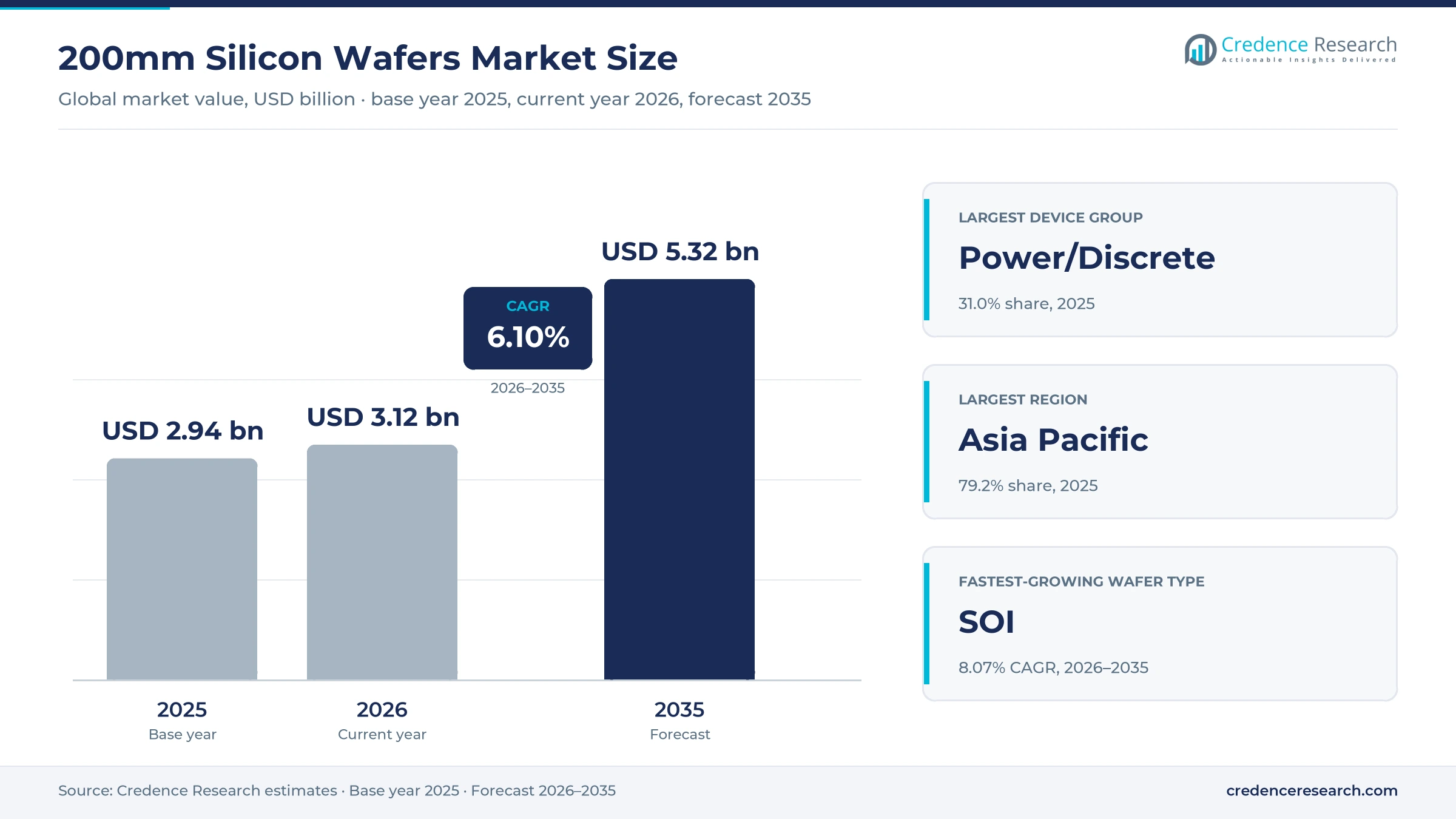
Credence Research values the 200mm silicon wafers market at USD 2.94 billion in 2025 and projects USD 5.32 billion by 2035, a 6.10% CAGR over 2026–2035, with USD 3.12 billion expected in 2026. Eight-inch wafers remain the workhorse substrate for power transistors, analog chips, microcontrollers and sensors, even as leading-edge logic and memory moved to 300mm long ago.
Growth is steady rather than fast. Demand tracks the capacity of more than 200 high-volume 200mm fabs, many of them in China, and the mix of power and automotive chips they run.
What does the market cover?
The market covers silicon wafers of 200mm (8-inch) diameter sold to chipmakers and foundries. The scope includes:
- Prime polished, epitaxial, annealed, silicon-on-insulator (SOI) and specialty silicon wafers.
- Test and monitor wafers, and reclaimed wafers returned to service after cleaning and polishing.
- Wafers grown by the Czochralski, magnetic Czochralski and float-zone methods.
The scope excludes 300mm and 150mm-and-smaller wafers, silicon carbide and gallium nitride wafers, polysilicon and ingots sold without slicing. Values are wafer sales in USD billion at current prices, allocated to the region where the wafers are consumed. The 200mm band is one slice of the wider silicon wafers market.
How was the estimate built?
All figures are Credence Research estimates, built from 200mm fab capacity, typical wafer starts per device type and published wafer price trends, and checked against supplier disclosures.
What do the public indicators show?
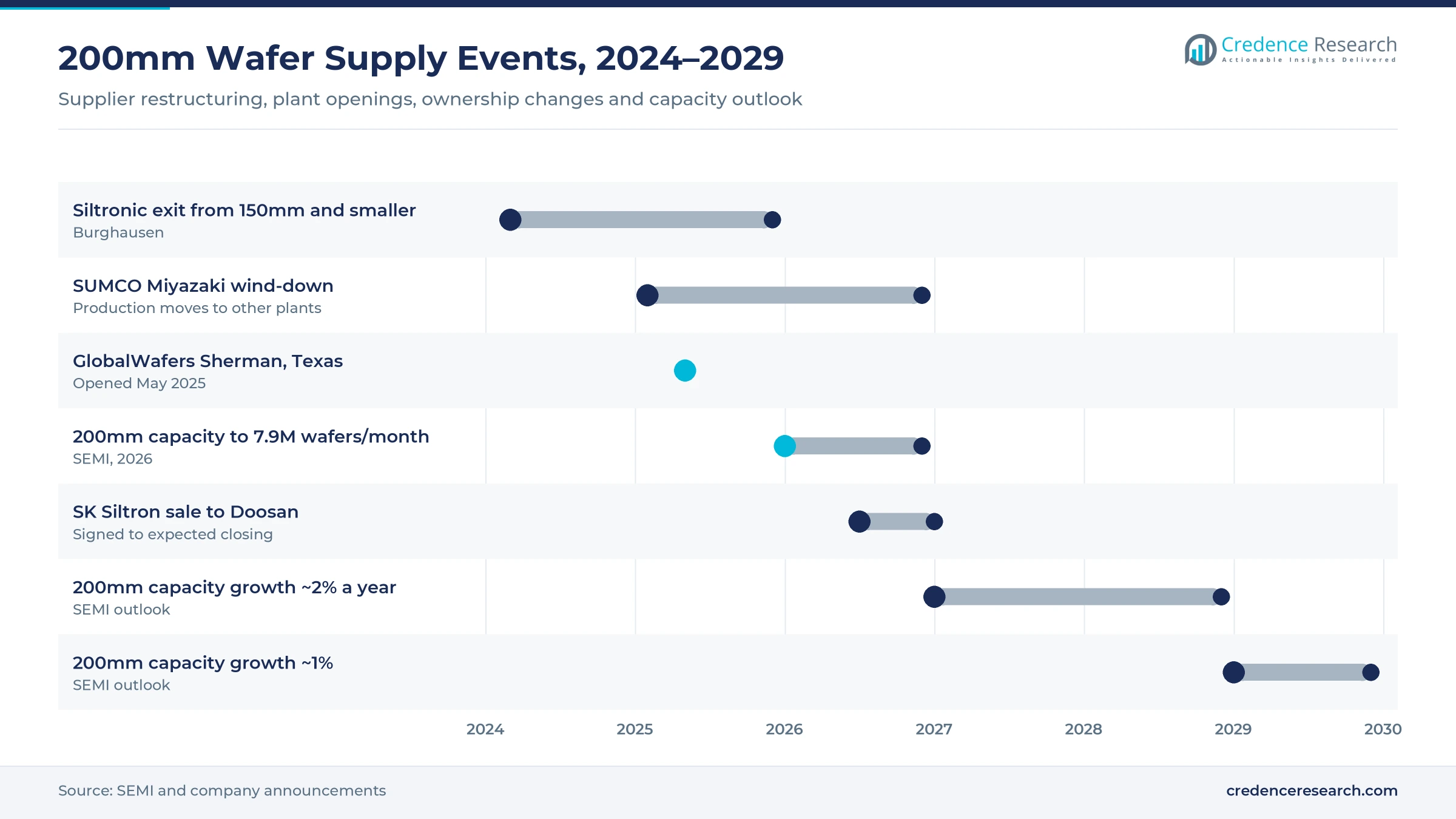
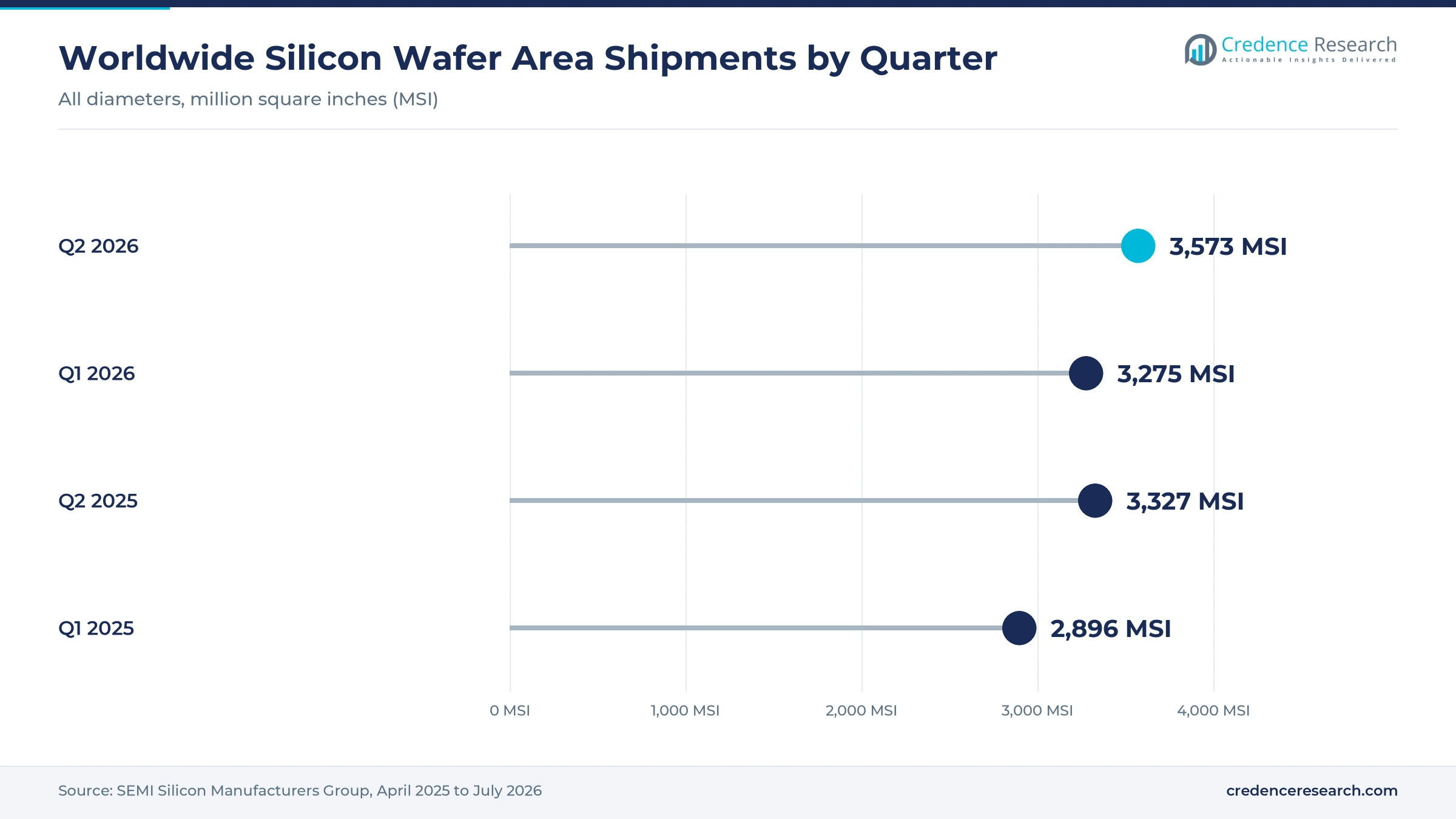
Global 200mm fab capacity is set to reach 7.9 million wafers per month in 2026, up 3%, across 227 high-volume fabs including 16 new ones, according to the SEMI 200mm Fab Outlook. SEMI expects growth to slow to about 2% a year in 2027 and 2028 and 1% in 2029. Worldwide silicon wafer area shipments across all diameters reached 3,573 million square inches in the second quarter of 2026, up 7.4% from a year earlier.
Report Attributes
| Attribute | Details |
|---|---|
| Historical Period | 2018–2024 |
| Base Year | 2025 |
| Forecast Period | 2026–2035 |
| Market Size 2025 | USD 2.94 billion |
| Market Size 2026 (estimate) | USD 3.12 billion |
| Market Size 2035 (forecast) | USD 5.32 billion |
| CAGR (2026–2035) | 6.10% |
| Segments Covered | By Wafer Type, By Device, By Crystal Growth, By End Use, By Process/Application, By Grade |
| Regions Covered | North America, Europe, Asia Pacific, Latin America, Middle East & Africa |
| Companies Covered | Shin-Etsu Chemical Co., Ltd., SUMCO Corporation, GlobalWafers Co., Ltd., Siltronic AG, SK Siltron Co., Ltd., National Silicon Industry Group, Wafer Works Corporation |
200mm Silicon Wafers Market Insights
- The 200mm silicon wafers market was worth USD 2.94 billion in 2025 and is forecast to reach USD 5.32 billion by 2035, a 6.10% CAGR over 2026–2035.
- Credence Research estimates the market at USD 3.12 billion in 2026, the current year.
- Power and discrete devices lead with a 31.0% share and grow fastest at 7.06% a year.
- Automotive is the largest end use at 30.0% and also the fastest-growing at 7.02%.
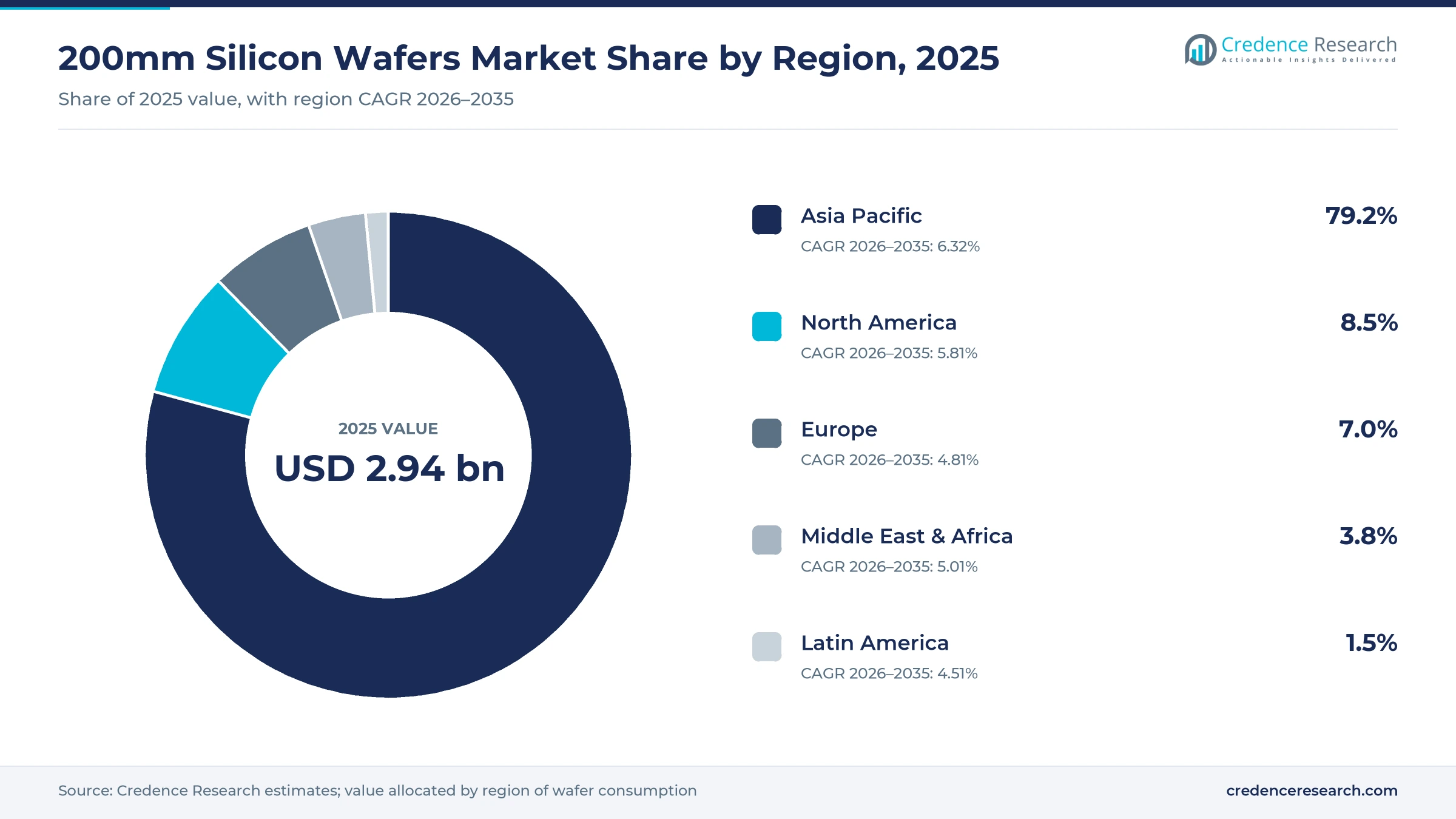
- Asia Pacific consumes 79.2% of 2025 value and grows fastest at 6.32%.
- Global 200mm fab capacity is set to reach 7.9 million wafers per month in 2026, according to SEMI.
Polished Wafers for Power and Automotive Chips Lead 200mm Value
Which wafer type leads?
Polished wafers lead with a 46.0% share in 2025, followed by epitaxial wafers. Annealed, SOI and specialty silicon wafers serve narrower needs. SOI grows fastest at 8.07% a year.
Which device group leads?
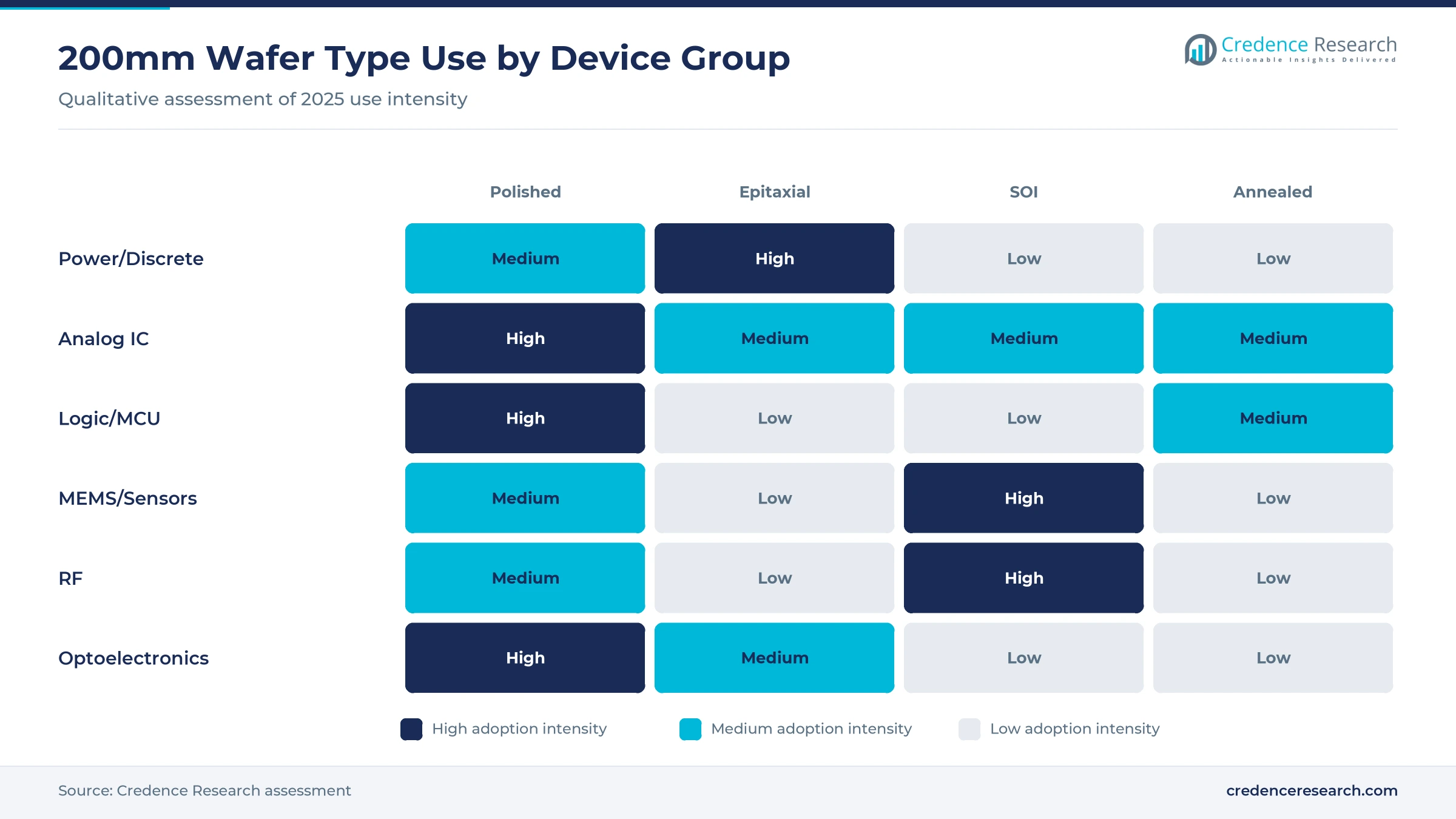
Power and discrete devices lead with a 31.0% share and grow fastest at 7.06% a year. Analog ICs, microcontrollers, MEMS and sensors, RF devices and optoelectronics form the rest of demand.
Which crystal growth method leads?
Standard Czochralski crystals lead with a 50.0% share. Float-zone crystals serve high-voltage power devices. Magnetic Czochralski grows fastest at 7.24% a year.
Which end use leads?
Automotive leads with a 30.0% share and grows fastest at 7.02% a year. Consumer electronics, industrial, telecom and healthcare electronics follow.
Which process family and grade lead?
Power processes lead by process family with a 28.0% share. Prime wafers lead by grade with a 74.0% share, while reclaimed wafers grow fastest at 6.75% a year as fabs cut costs on test runs. Epitaxial supply is covered in more depth in the epitaxial wafer market, and SOI in the silicon on insulator market.
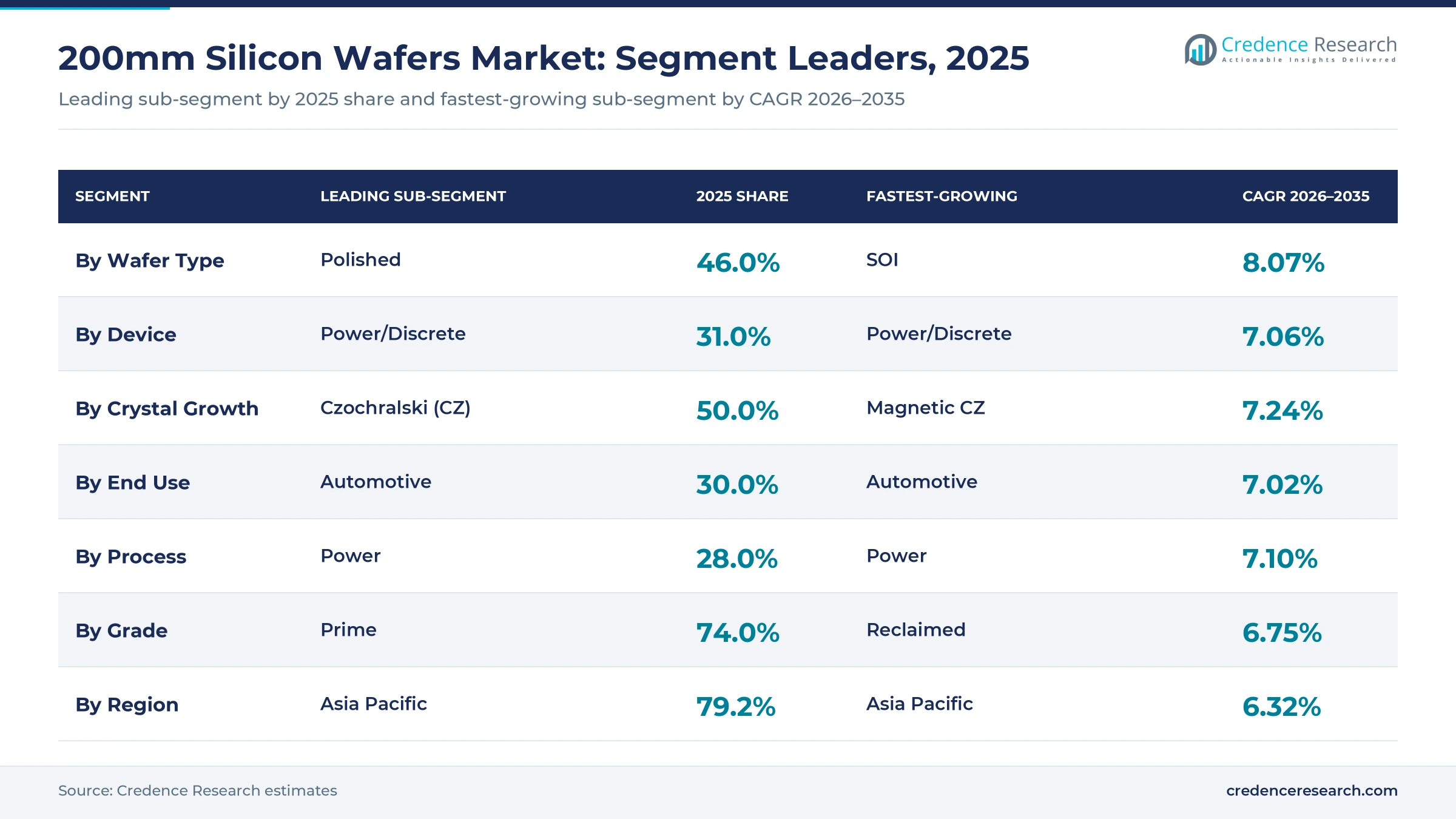
| Segment Group | Leading Sub-segment | 2025 Share | Fastest-growing Sub-segment | CAGR 2026–2035 |
|---|---|---|---|---|
| By Wafer Type | Polished | 46.0% | SOI | 8.07% |
| By Device | Power/Discrete | 31.0% | Power/Discrete | 7.06% |
| By Crystal Growth | Czochralski (CZ) | 50.0% | Magnetic CZ | 7.24% |
| By End Use | Automotive | 30.0% | Automotive | 7.02% |
| By Process/Application | Power | 28.0% | Power | 7.10% |
| By Grade | Prime | 74.0% | Reclaimed | 6.75% |
Request a Free Sample
Fill in your details and we'll send you a free sample report.
- Sample data tables & charts
- Research methodology
Mature-Node Chips, New Eight-Inch Fabs and Vehicle Electronics Keep Demand Steady
Why does mature-node demand matter most? (~+1.8% impact on forecast CAGR)
Sustained demand for power, analog, MEMS and microcontroller devices made on mature nodes is the strongest driver, adding an estimated 1.8 percentage points to the forecast CAGR. These chips do not benefit from smaller transistors, so chipmakers keep making them on depreciated 200mm lines where costs are low. Power and discrete devices lead device demand with a 31.0% share of 2025 value and are the fastest-growing device group at 7.06% a year. SEMI's industry group noted in July 2026 that AI demand is spreading to power devices and photonics. The limit is migration: as some power and analog makers move high-volume parts to 300mm, part of this demand shifts out of the 200mm market.
How do new fabs and localization add demand? (~+1.4% impact on forecast CAGR)
200mm fab additions and the localization of mature-node capacity add about 1.4 percentage points to the forecast CAGR. Governments in China, the United States, Europe and Southeast Asia fund domestic chip supply, and mature-node lines are the cheapest and fastest to build. Each new line needs a qualified wafer supply, often from more than one vendor, and qualification ties the fab to its chosen suppliers for years. The condition is utilization: new fabs buy wafers only when they load their tools, and capacity growth is expected to slow after 2026.
Why do vehicles and factories matter? (~+1.1% impact on forecast CAGR)
Automotive electrification and industrial electronics add about 1.1 percentage points to the forecast CAGR. An electric vehicle uses far more power semiconductors, battery-management chips and sensors than a combustion car, and most of them are made on 200mm wafers. Automotive is the largest end use with a 30.0% share and also the fastest-growing at 7.02% a year. Industrial automation and renewable-energy inverters add similar demand. The risk is cyclical: inventory corrections in automotive and industrial markets can cut wafer orders for several quarters, as happened in 2024 and 2025.
Epitaxial and SOI Wafers Gain as Suppliers Rationalize Small-Diameter Lines
Trend 1: Are higher-value wafers gaining share?
Yes. Epitaxial wafers serve most power devices, and SOI wafers suit RF switches, automotive chips and MEMS. SOI is the fastest-growing wafer type at 8.07% a year, while polished wafers lead with a 46.0% share.
Trend 2: Are suppliers closing older lines?
Yes. Siltronic completed its exit from wafers of 150mm and smaller at Burghausen in 2025, and SUMCO announced in February 2025 that it would end wafer production at its Miyazaki plant by the end of 2026. These moves concentrate supply on 200mm and 300mm and support pricing for the remaining 200mm capacity.
Trend 3: Is ownership consolidating?
SK Inc. agreed in July 2026 to sell 70.6% of SK Siltron, a 300mm and 200mm wafer maker, to Doosan for KRW 2.3 trillion, with closing expected in January 2027, as reported by Digital Today. Changes of ownership can shift investment priorities between diameters.
Trend 4: Is magnetic Czochralski growth spreading?
Magnetic Czochralski crystals offer lower oxygen content and better uniformity for power devices. They are the fastest-growing growth method at 7.24% a year, while standard Czochralski leads with a 50.0% share.
High Inventories, Slower Capacity Growth and Migration to 300mm Weigh on Prices
Why are inventories a problem?
Customers built large wafer stocks during the 2021–2022 shortage. Siltronic said in its first-quarter 2026 results that 200mm inventories remained persistently high, especially among power device customers. Wafer makers face lower volumes and price pressure until those stocks are used up.
Is 200mm capacity growth slowing?
Yes. SEMI expects 200mm capacity growth to fall from 3% in 2026 to about 1% by 2029. Slower capacity growth caps volume growth for wafer suppliers after the current wave of new fabs.
Why is migration to 300mm a threat?
Large power and analog makers have opened 300mm lines for high-volume products to lower cost per chip. Each migration removes 200mm wafer demand permanently. Smaller fabs and specialty devices stay on 200mm, so the market keeps growing, but more slowly than chip demand.
How does price competition affect suppliers?
Chinese wafer makers have added 200mm capacity with state support, raising competition for standard polished wafers. Suppliers with higher-value epitaxial and SOI products are less exposed.
Where are the opportunities?
New 200mm fabs in Southeast Asia, India and the United States need qualified local wafer supply. Suppliers that offer epitaxial and SOI wafers with short logistics can win these customers. The execution risk is qualification time, which can take a year or more per product.
Asia Pacific Consumes Four of Every Five 200mm Wafers
Value is allocated to the region where wafers are consumed in fabs.
| Region | Share 2025 | CAGR 2026–2035 |
|---|---|---|
| Asia Pacific | 79.2% | 6.32% |
| North America | 8.5% | 5.81% |
| Europe | 7.0% | 4.81% |
| Middle East & Africa | 3.8% | 5.01% |
| Latin America | 1.5% | 4.51% |
Why does Asia Pacific dominate?
Asia Pacific holds a 79.2% share in 2025 and is the fastest-growing region at 6.32% a year. China has the largest 200mm fab base and keeps adding mature-node capacity for domestic power and analog chips. Taiwan, Japan, South Korea and Southeast Asia host large foundries and integrated device makers, and Japan and South Korea are home to major wafer suppliers.
What drives North America?
North America holds 8.5% and grows at 5.81% a year. Analog, power and MEMS makers run 200mm fabs in the United States, and federal incentives support new mature-node capacity. GlobalWafers opened its Sherman, Texas, site in May 2025 and plans a second phase, according to DatacenterDynamics.
What shapes Europe?
Europe holds 7.0% and grows at 4.81% a year. Automotive and industrial chipmakers in Germany, France, Italy and Austria rely on 200mm lines, while some have moved high-volume power products to 300mm.
What about Latin America and the Middle East & Africa?
Latin America holds 1.5% and grows at 4.51%, with small specialty and assembly-related demand. The Middle East & Africa region holds 3.8% and grows at 5.01%, led by Israel's analog and specialty fabs and new semiconductor programs in the Gulf.
Shipment Data, Supplier Results and Ownership Changes, 2025–2026
| Development | Status and why it matters |
|---|---|
| In August 2026, SUMCO reported that shipments of 200mm and smaller wafers increased in the second quarter and expected a gradual recovery in the third quarter. | Reported. Signals the end of the inventory correction. |
| In July 2026, SEMI announced worldwide silicon wafer shipments of 3,573 million square inches in the second quarter of 2026, up 7.4% year on year. | Published. Confirms a broad wafer recovery. |
| In July 2026, SK Inc. signed an agreement to sell 70.6% of SK Siltron to Doosan for KRW 2.3 trillion, with closing expected in January 2027. | Announced. Changes ownership of a major 200mm supplier. |
| In April 2026, Siltronic announced first-quarter sales of EUR 306.5 million and said 200mm inventories remained high. | Reported. Shows continued pressure on 200mm volumes. |
| In February 2026, Siltronic announced 2026 guidance with sales down by a mid-single-digit percentage, citing declining 200mm demand. | Announced. Sets a cautious tone for 2026. |
| In January 2026, GlobalWafers announced plans for a second phase at Sherman, Texas, and a conversion of its epitaxy facility there to silicon carbide. | Planned. Expands US wafer capacity. |
| In May 2025, GlobalWafers opened its Sherman, Texas, wafer site. | Opened. Adds US-based wafer supply. |
| In February 2025, SUMCO announced it would end wafer production at its Miyazaki plant by the end of 2026, moving output to other plants. | Announced. Rationalizes small-diameter supply. |
Need a Custom Version of This Report?
Tailor the scope, geography, or segments to your exact requirements.
- Custom geography or segment scope
- Direct access to our analyst team
Five Global Wafer Makers Face Rising Chinese Competition
The 200mm wafer business is concentrated. A few global suppliers serve most qualified fabs, and Chinese suppliers are gaining domestic share. No share ranking is given because suppliers do not report 200mm sales separately in a comparable way.
Who are the global suppliers?
Shin-Etsu Chemical Co., Ltd. and SUMCO Corporation of Japan are the two largest silicon wafer makers, and both supply 200mm wafers alongside 300mm. SUMCO reports its 200mm-and-smaller shipments separately and said they increased in the second quarter of 2026. GlobalWafers Co., Ltd. of Taiwan runs plants in Asia, the United States and Europe. Siltronic AG of Germany produces 200mm and 300mm wafers after exiting smaller diameters. SK Siltron Co., Ltd. of South Korea makes 300mm and 200mm wafers and is being sold to Doosan.
Who are the regional challengers?
National Silicon Industry Group leads China's push for domestic wafer supply, with subsidiaries that make 200mm and 300mm wafers, including SOI. Wafer Works Corporation of Taiwan focuses on 200mm and smaller polished and epitaxial wafers for power and discrete devices.
How do suppliers compete?
Suppliers compete on quality consistency, epitaxial and SOI capability, and long-term supply agreements. Qualification takes months, so customers rarely switch suppliers quickly, which protects incumbents. Chinese suppliers compete on price and on government-backed customer relationships.
How are suppliers responding?
Global suppliers are shifting investment to 300mm while running 200mm lines for cash, closing smaller-diameter lines and adding higher-value products. Equipment for these lines is covered in the wafer processing equipment market.
Frequently Asked Questions
How big is the 200mm silicon wafers market?
Why are 200mm wafers still used?
What drives demand for 200mm wafers?
Which wafer type grows fastest?
Which region consumes the most 200mm wafers?
Who are the main suppliers?
Table of Content
Chapter 1 Market Segmentation
- 1.1 Segmentation Framework
- 1.1.1 Product and Service Classification
- 1.1.2 Application and End-Use Classification
- 1.1.3 Technology and Solution Classification
- 1.1.4 Customer and Distribution Channel Classification
- 1.1.5 Geographic Segmentation
- 1.1.6 Market Segment Definitions and Boundaries
- 1.2 By Wafer Type
- 1.2.1 Polished
- 1.2.2 Epitaxial
- 1.2.3 Annealed
- 1.2.4 SOI
- 1.2.5 Specialty Silicon
- 1.3 By Device
- 1.3.1 Power/Discrete
- 1.3.2 Analog IC
- 1.3.3 Logic/MCU
- 1.3.4 MEMS/Sensors
- 1.3.5 RF
- 1.3.6 Optoelectronics
- 1.4 By Crystal Growth
- 1.4.1 Czochralski (CZ)
- 1.4.2 Magnetic CZ
- 1.4.3 Float Zone (FZ)
- 1.5 By End Use
- 1.5.1 Automotive
- 1.5.2 Consumer Electronics
- 1.5.3 Industrial
- 1.5.4 Telecom
- 1.5.5 Healthcare
- 1.6 By Process/Application
- 1.6.1 Power
- 1.6.2 Mature Logic
- 1.6.3 BCD/Analog
- 1.6.4 MEMS
- 1.6.5 Specialty Devices
- 1.7 By Grade
- 1.7.1 Prime
- 1.7.2 Test/Monitor
- 1.7.3 Reclaimed
Chapter 2 Introduction
- 2.1 Report Objectives and Scope
- 2.2 Product Definition and Industry Terminology
- 2.3 Market Inclusions and Exclusions
- 2.4 Research Process
- 2.4.1 Primary Research and Expert Interviews
- 2.4.2 Secondary Research and Source Review
- 2.4.3 Top-Down and Bottom-Up Estimation
- 2.4.4 Data Triangulation and Verification
- 2.5 Market Size Measurement Basis
- 2.5.1 2025: USD 2.94 billion → 2035: USD 5.32 billion
- 2.6 Historical and Forecast Reference Periods
- 2.6.1 Historical Period: 2018-2025
- 2.6.2 Base Year: 2025
- 2.6.3 Forecast Period: 2025-2035
- 2.7 Research Assumptions and Limitations
Chapter 3 Executive Summary
- 3.1 Market Snapshot and Key Findings
- 3.2 Base-Year Market Size, 2025
- 3.3 Forecast Market Size, 2035
- 3.4 Revenue and Volume Growth Outlook
- 3.5 Key Demand and Supply Indicators
- 3.6 Leading Market Segments
- 3.7 Fastest-Growing Market Opportunities
- 3.8 Regional Performance Highlights
- 3.9 Technology and Industry Transformation
- 3.10 Competitive Landscape Summary
- 3.11 Analyst View and Strategic Implications
Chapter 4 Global 200mm Silicon Wafers Market Trends and Developments
- 4.1 Historical Industry Development, 2018-2025
- 4.2 Recent Market Trends and Developments
- 4.3 Demand and Customer Behavior Trends
- 4.4 Technology and Product Innovation
- 4.5 Artificial Intelligence, Automation and Digitalization
- 4.6 Local Manufacturing and Supply Chain Realignment
- 4.7 Industry Partnerships, Mergers and Acquisitions
- 4.8 Sustainability and Circular Economy Developments
- 4.9 Government and Private Sector Investment Trends
- 4.10 Emerging Business Models and Commercialization
- 4.11 Industry Developments and Announcements
Chapter 5 Global 200mm Silicon Wafers Market Production, Supply and Demand Analysis
- 5.1 Demand Trend and Consumption Analysis, 2018-2025
- 5.2 Demand Forecast, 2025-2035
- 5.3 Production and Output Trend, 2018-2025
- 5.4 Production and Output Forecast, 2025-2035
- 5.5 Installed Capacity and Capacity Utilization
- 5.6 Company-Wise Production Plants and Statistics
- 5.6.1 Installed Production Capacity
- 5.6.2 Actual Production
- 5.6.3 Planned Capacity and Expansion Targets
- 5.7 Supply Chain Structure and Procurement Trends
- 5.8 Supply-Demand Gap and Bottlenecks
- 5.9 Import Dependence and Sourcing Structure
- 5.10 Contract Manufacturing and Outsourcing
- 5.11 Regional Supply and Demand Concentration
Chapter 6 Global 200mm Silicon Wafers Market Pricing Analysis
- 6.1 Pricing Structure and Measurement
- 6.2 Historical Pricing Trends, 2018-2025
- 6.3 Pricing Outlook, 2025-2035
- 6.4 Average Selling Price and Unit Economics
- 6.5 Pricing by Product and Market Segment
- 6.6 Geographic Pricing Differences
- 6.7 Key Input, Energy, Labor and Logistics Costs
- 6.8 Contract Pricing and Purchasing Models
- 6.9 Pricing Sensitivity and Competitive Positioning
- 6.10 Price, Margin and Profitability Implications
Chapter 7 Global 200mm Silicon Wafers Market Dynamics
- 7.1 Market Growth Drivers
- 7.1.1 Demand-Side Drivers
- 7.1.2 Technology and Innovation Drivers
- 7.1.3 Infrastructure and Investment Drivers
- 7.1.4 Regulatory and Policy Drivers
- 7.2 Market Restraints
- 7.2.1 Cost and Affordability Constraints
- 7.2.2 Technology and Adoption Barriers
- 7.2.3 Supply Chain and Operational Constraints
- 7.3 Market Challenges
- 7.3.1 Competitive Pressure and Margin Erosion
- 7.3.2 Skills, Infrastructure and Implementation Gaps
- 7.4 Emerging Market Opportunities
- 7.5 Market Dynamics Impact and Time-Horizon Assessment
Chapter 8 Global 200mm Silicon Wafers Value Chain Analysis
- 8.1 Industry Value Chain Overview
- 8.2 Upstream Suppliers and Critical Inputs
- 8.3 Technology and Component Providers
- 8.4 Manufacturing or Service Delivery
- 8.5 Distribution, Channel Partners and Integrators
- 8.6 Downstream Applications and End Users
- 8.7 Value Addition and Profit Pools
- 8.8 Vertical Integration and Outsourcing
- 8.9 Supplier Concentration and Risk
- 8.10 Supply Chain Localization and Resilience
Chapter 9 Global 200mm Silicon Wafers Market Regulations and Policies
- 9.1 Relevant Laws, Standards and Compliance Frameworks
- 9.2 Product, Service, Safety and Quality Requirements
- 9.3 Government Policies, Incentives and Subsidies
- 9.4 Imports, Exports and Trade Barriers
- 9.5 Public Procurement and Local Content Requirements
- 9.6 Environmental and Sustainability Compliance
- 9.7 Upcoming Policy Changes and Market Implications
Chapter 10 Global 200mm Silicon Wafers Market Hotspots and Opportunities
- 10.1 Market Opportunity Mapping and Growth Hotspots
- 10.2 High-Growth Applications and Customer Groups
- 10.3 Underserved Markets and White-Space Opportunities
- 10.4 Emerging Technology and Product Opportunities
- 10.5 New Capacity and Investment Hotspots
- 10.6 Market Entry and Expansion Opportunities
- 10.7 Distribution and Partnership Opportunities
- 10.8 Near-Term and Long-Term Commercial Potential
- 10.9 Opportunity Attractiveness and Execution Risks
Chapter 11 Global 200mm Silicon Wafers Market Outlook, 2025-2035
- 11.1 Market Size and Analysis
- 11.1.1 Revenue (Market Measurement: 2025: USD 2.94 billion → 2035: USD 5.32 billion)
- 11.1.2 Market Volume and Quantity Sold
- 11.1.3 Historical Market Size, 2018-2025
- 11.1.4 Base-Year Market Size, 2025
- 11.2 Market Forecast, 2025-2035
- 11.2.1 Revenue Forecast to 2035
- 11.2.2 Volume Forecast to 2035
- 11.2.3 CAGR and Year-on-Year Growth
- 11.2.4 Incremental Revenue Opportunity
- 11.3 Forecast Assumptions and Scenario Analysis
- 11.3.1 Base-Case Forecast
- 11.3.2 Optimistic and Conservative Scenarios
- 11.3.3 Technology, Pricing and Policy Sensitivities
- 11.4 Market Attractiveness and Growth Outlook
Chapter 12 Global 200mm Silicon Wafers Market Segmentation and Outlook
- 12.1 Segmentation Summary and Market Shares, 2025
- 12.2 Largest and Fastest-Growing Segments
- 12.3 By Wafer Type - Market Size and Forecast, 2025-2035
- 12.3.1 Segment Definition and Scope
- 12.3.2 Historical Market Size, 2018-2025
- 12.3.3 Revenue Forecast, 2025-2035
- 12.3.4 Volume Forecast, 2025-2035
- 12.3.5 Base-Year Market Share, 2025
- 12.3.6 Segment CAGR and Growth Drivers
- 12.3.7 Subsegment Market Size and Forecast
- 12.3.7.1 Polished
- 12.3.7.2 Epitaxial
- 12.3.7.3 Annealed
- 12.3.7.4 SOI
- 12.3.7.5 Specialty Silicon
- 12.3.8 Subsegment Pricing and Adoption Trends
- 12.3.9 Leading Suppliers and Competition
- 12.3.10 Regional Demand and Opportunities
- 12.4 By Device - Market Size and Forecast, 2025-2035
- 12.4.1 Segment Definition and Scope
- 12.4.2 Historical Market Size, 2018-2025
- 12.4.3 Revenue Forecast, 2025-2035
- 12.4.4 Volume Forecast, 2025-2035
- 12.4.5 Base-Year Market Share, 2025
- 12.4.6 Segment CAGR and Growth Drivers
- 12.4.7 Subsegment Market Size and Forecast
- 12.4.7.1 Power/Discrete
- 12.4.7.2 Analog IC
- 12.4.7.3 Logic/MCU
- 12.4.7.4 MEMS/Sensors
- 12.4.7.5 RF
- 12.4.7.6 Optoelectronics
- 12.4.8 Subsegment Pricing and Adoption Trends
- 12.4.9 Leading Suppliers and Competition
- 12.4.10 Regional Demand and Opportunities
- 12.5 By Crystal Growth - Market Size and Forecast, 2025-2035
- 12.5.1 Segment Definition and Scope
- 12.5.2 Historical Market Size, 2018-2025
- 12.5.3 Revenue Forecast, 2025-2035
- 12.5.4 Volume Forecast, 2025-2035
- 12.5.5 Base-Year Market Share, 2025
- 12.5.6 Segment CAGR and Growth Drivers
- 12.5.7 Subsegment Market Size and Forecast
- 12.5.7.1 Czochralski (CZ)
- 12.5.7.2 Magnetic CZ
- 12.5.7.3 Float Zone (FZ)
- 12.5.8 Subsegment Pricing and Adoption Trends
- 12.5.9 Leading Suppliers and Competition
- 12.5.10 Regional Demand and Opportunities
- 12.6 By End Use - Market Size and Forecast, 2025-2035
- 12.6.1 Segment Definition and Scope
- 12.6.2 Historical Market Size, 2018-2025
- 12.6.3 Revenue Forecast, 2025-2035
- 12.6.4 Volume Forecast, 2025-2035
- 12.6.5 Base-Year Market Share, 2025
- 12.6.6 Segment CAGR and Growth Drivers
- 12.6.7 Subsegment Market Size and Forecast
- 12.6.7.1 Automotive
- 12.6.7.2 Consumer Electronics
- 12.6.7.3 Industrial
- 12.6.7.4 Telecom
- 12.6.7.5 Healthcare
- 12.6.8 Subsegment Pricing and Adoption Trends
- 12.6.9 Leading Suppliers and Competition
- 12.6.10 Regional Demand and Opportunities
- 12.7 By Process/Application - Market Size and Forecast, 2025-2035
- 12.7.1 Segment Definition and Scope
- 12.7.2 Historical Market Size, 2018-2025
- 12.7.3 Revenue Forecast, 2025-2035
- 12.7.4 Volume Forecast, 2025-2035
- 12.7.5 Base-Year Market Share, 2025
- 12.7.6 Segment CAGR and Growth Drivers
- 12.7.7 Subsegment Market Size and Forecast
- 12.7.7.1 Power
- 12.7.7.2 Mature Logic
- 12.7.7.3 BCD/Analog
- 12.7.7.4 MEMS
- 12.7.7.5 Specialty Devices
- 12.7.8 Subsegment Pricing and Adoption Trends
- 12.7.9 Leading Suppliers and Competition
- 12.7.10 Regional Demand and Opportunities
- 12.8 By Grade - Market Size and Forecast, 2025-2035
- 12.8.1 Segment Definition and Scope
- 12.8.2 Historical Market Size, 2018-2025
- 12.8.3 Revenue Forecast, 2025-2035
- 12.8.4 Volume Forecast, 2025-2035
- 12.8.5 Base-Year Market Share, 2025
- 12.8.6 Segment CAGR and Growth Drivers
- 12.8.7 Subsegment Market Size and Forecast
- 12.8.7.1 Prime
- 12.8.7.2 Test/Monitor
- 12.8.7.3 Reclaimed
- 12.8.8 Subsegment Pricing and Adoption Trends
- 12.8.9 Leading Suppliers and Competition
- 12.8.10 Regional Demand and Opportunities
- 12.9 Segment Growth Comparison
- 12.10 Segment Attractiveness and Priority Matrix
Chapter 13 Global 200mm Silicon Wafers End-Use and Application Market Outlook
- 13.1 End-Use Industry and Customer Demand Structure
- 13.2 Leading Applications and Customer Groups
- 13.3 End-Use Market Size, Share and Forecast
- 13.4 Major End-Use Industry Deep Dives
- 13.4.1 Customer Requirements and Use Cases
- 13.4.2 Demand and Replacement Cycles
- 13.4.3 Technical and Regulatory Considerations
- 13.4.4 Purchasing and Procurement Models
- 13.4.5 Leading Vendors and Distribution Channels
- 13.4.6 Forecast and Commercial Opportunities
- 13.5 Emerging Applications and Cross-Segment Demand
- 13.6 End-Use Industry Investment Priorities
Chapter 14 Global 200mm Silicon Wafers Geographic Market Outlook, 2025-2035
- 14.1 Regional Market Size and Share, 2025
- 14.2 Regional Market Forecast, 2025-2035
- 14.3 Regional Pricing, Production and Demand Differences
- 14.4 North America
- 14.4.1 United States
- 14.4.2 Canada
- 14.4.3 Mexico
- 14.5 Europe
- 14.5.1 Germany
- 14.5.2 France
- 14.5.3 Italy
- 14.5.4 United Kingdom
- 14.5.5 Spain
- 14.5.6 Poland
- 14.5.7 Russia
- 14.5.8 Netherlands
- 14.5.9 Belgium
- 14.5.10 Sweden
- 14.5.11 Denmark
- 14.5.12 Norway
- 14.5.13 Rest of Europe
- 14.6 Asia Pacific
- 14.6.1 China
- 14.6.2 India
- 14.6.3 Japan
- 14.6.4 South Korea
- 14.6.5 Thailand
- 14.6.6 Indonesia
- 14.6.7 Vietnam
- 14.6.8 Malaysia
- 14.6.9 Australia
- 14.6.10 Rest of Asia Pacific
- 14.7 Latin America
- 14.7.1 Brazil
- 14.7.2 Argentina
- 14.7.3 Colombia
- 14.7.4 Chile
- 14.7.5 Rest of Latin America
- 14.8 Middle East
- 14.8.1 Saudi Arabia
- 14.8.2 United Arab Emirates
- 14.8.3 Turkey
- 14.8.4 Israel
- 14.8.5 Iran
- 14.8.6 Rest of the Middle East
- 14.9 Africa
- 14.9.1 South Africa
- 14.9.2 Egypt
- 14.9.3 Nigeria
- 14.9.4 Morocco
- 14.9.5 Rest of Africa
- 14.10 Regional Investment, Policy and Supply Chain Differences
- 14.11 Regional Competitive Landscape
- 14.12 Geographic Growth Hotspots
Chapter 15 Global 200mm Silicon Wafers Technology, Innovation and Sustainability Outlook
- 15.1 Technology Landscape and Maturity
- 15.2 Product, Process and Service Innovation
- 15.3 AI, Automation and Digital Tools in the Industry
- 15.4 Technology Adoption and Performance Benchmarking
- 15.5 Innovation Pipeline and R&D Investment
- 15.6 Patent and Intellectual Property Trends
- 15.7 Energy Efficiency and Resource Management
- 15.8 Sustainability, Recycling and Circularity
- 15.9 Technology Roadmap, 2025-2035
- 15.10 Risks of Obsolescence and Technology Substitution
Chapter 16 Global 200mm Silicon Wafers Market Key Strategic Imperatives
- 16.1 Growth and Market Entry Priorities
- 16.2 High-Return Products and Segments
- 16.3 Pricing, Profitability and Cost Optimization
- 16.4 Technology Investment and Product Differentiation
- 16.5 Supply Chain Localization and Resilience
- 16.6 Distribution and Customer Acquisition
- 16.7 Partnership, Acquisition and Capacity Strategy
- 16.8 Regional Expansion Priorities
- 16.9 Short-, Medium- and Long-Term Actions
Chapter 17 Competition Outlook
- 17.1 Industry Competition Characteristics
- 17.2 Market Structure and Concentration
- 17.3 Market Share and Competitive Positioning, 2025
- 17.4 Company-Wise Revenue and Product Benchmarking
- 17.5 Production and Service Capacity Benchmarking
- 17.6 Technology, Pricing and Differentiation
- 17.7 Regional Footprint and Distribution Strength
- 17.8 Mergers, Acquisitions and Strategic Alliances
- 17.9 New Entrants and Competitive Threats
- 17.10 Porter's Five Forces and Industry Attractiveness
- 17.11 Competitive Outlook, 2025-2035
Chapter 18 Company Profiles
- 18.1 Company Coverage and Selection Criteria
- 18.2 Shin-Etsu Chemical Co., Ltd.
- 18.2.1 Business Description
- 18.2.2 Company Ownership and Geographic Presence
- 18.2.3 Product and Service Portfolio
- 18.2.4 Manufacturing and Operating Footprint
- 18.2.5 Production Capacity and Expansion Plans
- 18.2.6 Financial Performance and Investment
- 18.2.7 Market Share and Competitive Position
- 18.2.8 Technology and Innovation Capabilities
- 18.2.9 Strategic Alliances or Partnerships
- 18.2.10 Recent Developments
- 18.2.11 Growth Strategy and Outlook
- 18.3 SUMCO Corporation
- 18.4 GlobalWafers Co., Ltd.
- 18.5 Siltronic AG
- 18.6 SK Siltron Co., Ltd.
- 18.7 National Silicon Industry Group
- 18.8 Wafer Works Corporation
- 18.9 Other Relevant Market Participants
Note: Every listed company is profiled on the structure shown under the first company. The company list is preliminary and may change based on research findings, market developments, data availability and client requirements.
Chapter 19 Disclaimer
- 19.1 Research and Forecast Disclaimer
- 19.2 Data Source and Estimation Limitations
Note: The depth of individual sections depends on data availability for this market. Volume, capacity, trade and other unit-based metrics are included where applicable.