2.5D and 3D Semiconductor Packaging Market: USD 11.15 billion in 2025, Driven by AI Accelerators
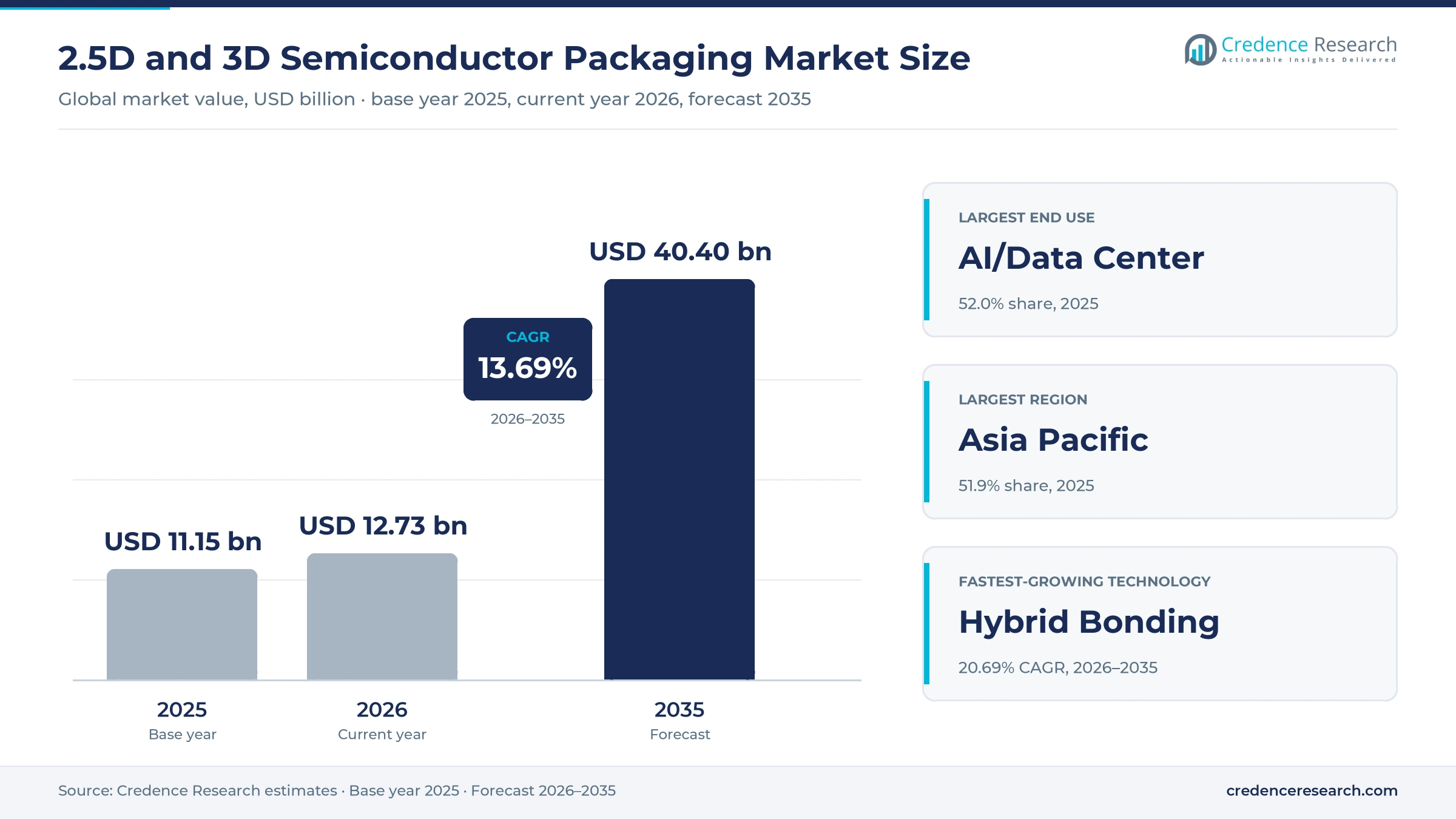
At USD 11.15 billion in 2025, the 2.5D and 3D semiconductor packaging market is on course for USD 40.40 billion by 2035, according to Credence Research, a 13.69% CAGR over 2026–2035. The 2026 estimate is USD 12.73 billion. Packaging has become a bottleneck for AI chips, because a modern accelerator is several dies and memory stacks joined on one interposer or substrate.
As transistor scaling slows and costs rise, chipmakers gain performance by stacking and placing dies side by side. That shifts value from the front-end fab to the package.
What does the market include?
The market covers packaging services and the associated interposers and substrates that join multiple dies in two-and-a-half or three dimensions. The scope includes:
- 2.5D packaging on silicon interposers, organic redistribution layers or embedded bridges, and fan-out on substrate.
- 3D stacking with through-silicon vias (TSV), hybrid bonding, and panel-level fan-out.
- Work done by foundries, outsourced assembly and test (OSAT) firms and integrated device makers (IDM).
The scope excludes conventional wire-bond and flip-chip packages with a single die, front-end wafer fabrication, the value of the dies themselves, and packaging equipment. Values are packaging revenue in USD billion at current prices, allocated by the region of the customer that buys the packaged device. The topic overlaps with the advanced semiconductor packaging market, which also counts single-die advanced packages.
How was the estimate built?
All figures are Credence Research estimates, built from disclosed advanced-packaging revenue, announced capacity, AI accelerator and HBM shipment trends, and typical packaging cost per device.
What do the indicators show?
ASE Technology said in a July 2026 filing on SEC Form 6-K that its leading-edge advanced packaging revenue was tracking ahead of USD 3.5 billion for 2026. SEMI forecasts assembly and packaging equipment sales of USD 6.7 billion in 2026 and USD 8.6 billion in 2028, as stated in its mid-year equipment forecast.
Report Attributes
| Attribute | Details |
|---|---|
| Historical Period | 2018–2024 |
| Base Year | 2025 |
| Forecast Period | 2026–2035 |
| Market Size 2025 | USD 11.15 billion |
| Market Size 2026 (estimate) | USD 12.73 billion |
| Market Size 2035 (forecast) | USD 40.40 billion |
| CAGR (2026–2035) | 13.69% |
| Segments Covered | By Packaging Technology, By Application, By Substrate, By End Use, By Integration, By Provider Type |
| Regions Covered | North America, Europe, Asia Pacific, Latin America, Middle East & Africa |
| Companies Covered | Taiwan Semiconductor Manufacturing Co., Samsung Electronics, Intel Corporation, ASE Technology Holding, Amkor Technology, JCET Group, SK hynix, Micron Technology |
2.5D and 3D Semiconductor Packaging Market Insights
- The 2.5D and 3D semiconductor packaging market was worth USD 11.15 billion in 2025 and is forecast to reach USD 40.40 billion by 2035, a 13.69% CAGR over 2026–2035.
- Credence Research estimates the market at USD 12.73 billion in 2026, the current year.
- AI accelerators and HBM are the strongest driver, adding about 4.2 percentage points to the forecast CAGR.
- 2.5D interposer packaging leads with a 46.0% share; hybrid bonding grows fastest at 20.69% a year.
- AI and data center products hold 52.0% of 2025 value and grow fastest at 16.20%.
- Asia Pacific is the largest region at 51.9%; the Middle East & Africa grows fastest at 15.39%.
Interposer-Based 2.5D Packaging for AI and HBM Leads Value
Which packaging technology leads?
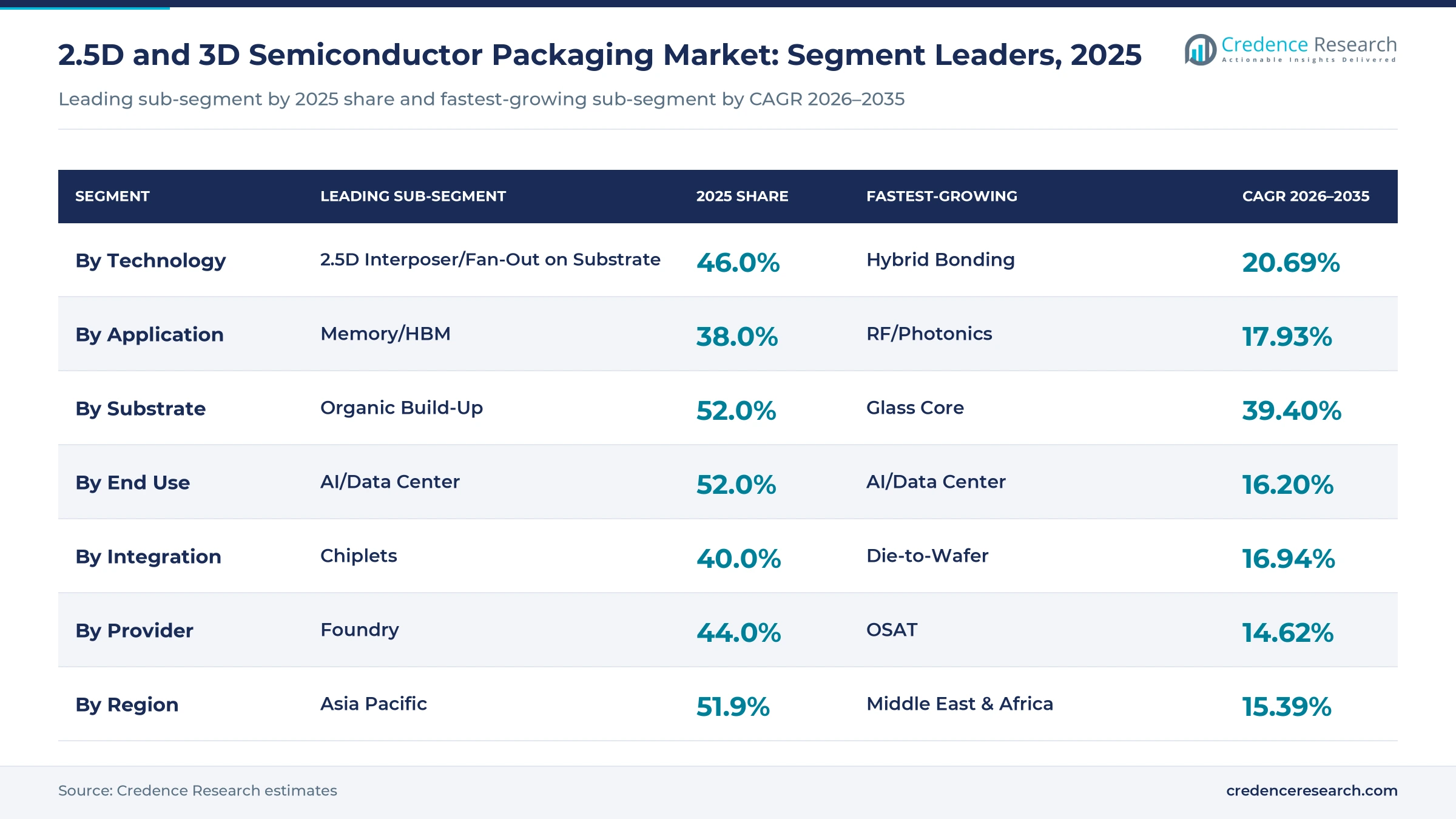
2.5D interposer and fan-out-on-substrate packaging leads with a 46.0% share in 2025. 3D TSV stacking, used mainly in HBM, follows. Hybrid bonding grows fastest at 20.69% a year.
Which application leads?
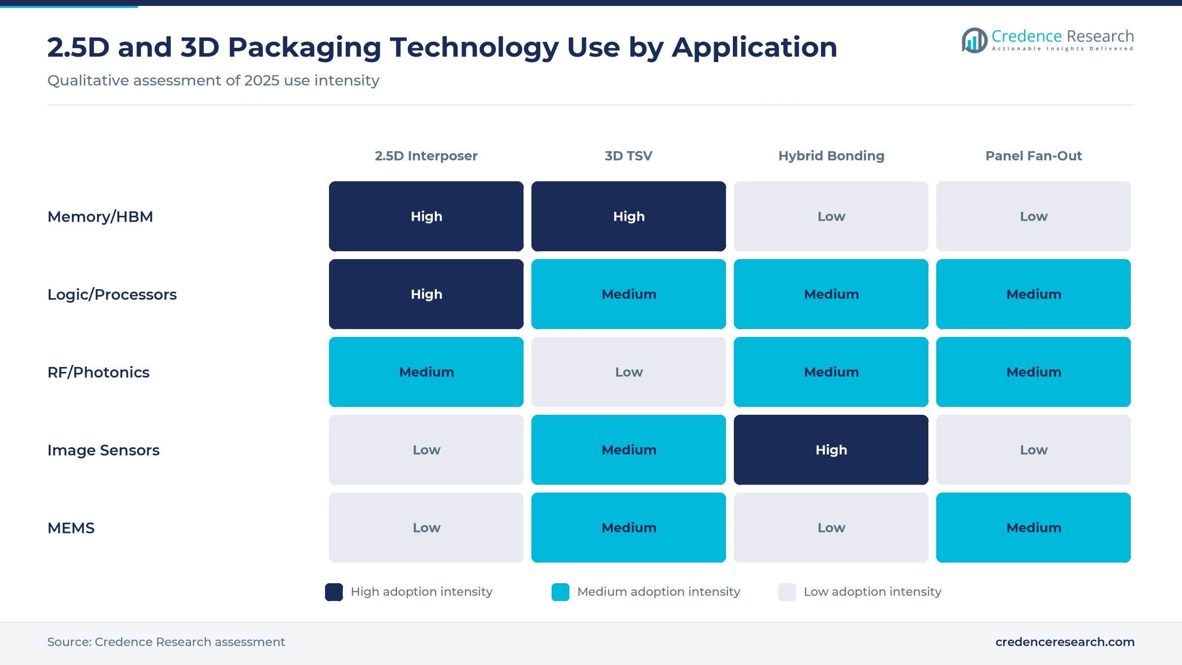
Memory and HBM lead with a 38.0% share, followed by logic and processors. Image sensors and MEMS use stacked designs at lower value per unit. RF and photonics grow fastest at 17.93% a year.
Which substrate leads?
Organic build-up substrates lead with a 52.0% share, while silicon interposers carry the highest-density designs. Ceramic substrates serve defense and harsh-environment uses. Glass cores grow fastest at 39.40% a year.
Which end use leads?
AI and data center products lead with a 52.0% share and grow fastest at 16.20% a year. Consumer electronics, automotive and ADAS, telecom, and aerospace and defense follow.
Which integration approach and provider lead?
Chiplets lead integration approaches with a 40.0% share, while die-to-wafer bonding grows fastest at 16.94% a year. Foundries lead providers with a 44.0% share; OSATs grow fastest at 14.62% a year as foundries outsource part of their packaging. See the chiplet packaging technology market for chiplet-specific detail.
| Segment Group | Leading Sub-segment | 2025 Share | Fastest-growing Sub-segment | CAGR 2026–2035 |
|---|---|---|---|---|
| By Packaging Technology | 2.5D Interposer/Fan-Out on Substrate | 46.0% | Hybrid Bonding | 20.69% |
| By Application | Memory/HBM | 38.0% | RF/Photonics | 17.93% |
| By Substrate | Organic Build-Up | 52.0% | Glass Core | 39.40% |
| By End Use | AI/Data Center | 52.0% | AI/Data Center | 16.20% |
| By Integration | Chiplets | 40.0% | Die-to-Wafer | 16.94% |
| By Provider Type | Foundry | 44.0% | OSAT | 14.62% |
Request a Free Sample
Fill in your details and we'll send you a free sample report.
- Sample data tables & charts
- Research methodology
AI Accelerators, Chiplet Designs and Record Packaging Investment Push Demand
Why are AI accelerators the main driver? (~+4.2% impact on forecast CAGR)
AI accelerators and high-bandwidth memory (HBM) stacks need ultra-high bandwidth between dies, and this is the strongest driver, adding an estimated 4.2 percentage points to the forecast CAGR. A data-center GPU places a large logic die next to several HBM stacks on an interposer, so every accelerator shipped requires 2.5D and 3D packaging. Each HBM stack is itself a 3D package of DRAM dies joined by through-silicon vias. AI and data-center products are the largest end use with a 52.0% share of 2025 value and the fastest-growing at 16.20% a year. The limit is capacity: interposer and HBM supply have constrained accelerator shipments since 2023, so revenue grows only as fast as new lines open.
How do chiplets change chip design? (~+3.1% impact on forecast CAGR)
Chiplet architectures and heterogeneous integration replacing monolithic chips add about 3.1 percentage points to the forecast CAGR. Designers split large chips into smaller dies made on the best node for each function, then join them in the package. AMD, Intel and Apple already ship multi-die processors, and cloud providers use chiplets in their custom AI chips. The UCIe Consortium released its 3.0 specification in August 2025 at 64 GT/s with more than 150 members, as announced on Business Wire. Chiplets lead integration approaches with a 40.0% share. The condition is design tools and test: known-good-die testing and thermal design remain harder for chiplet systems.
How much are foundries and OSATs investing? (~+2.4% impact on forecast CAGR)
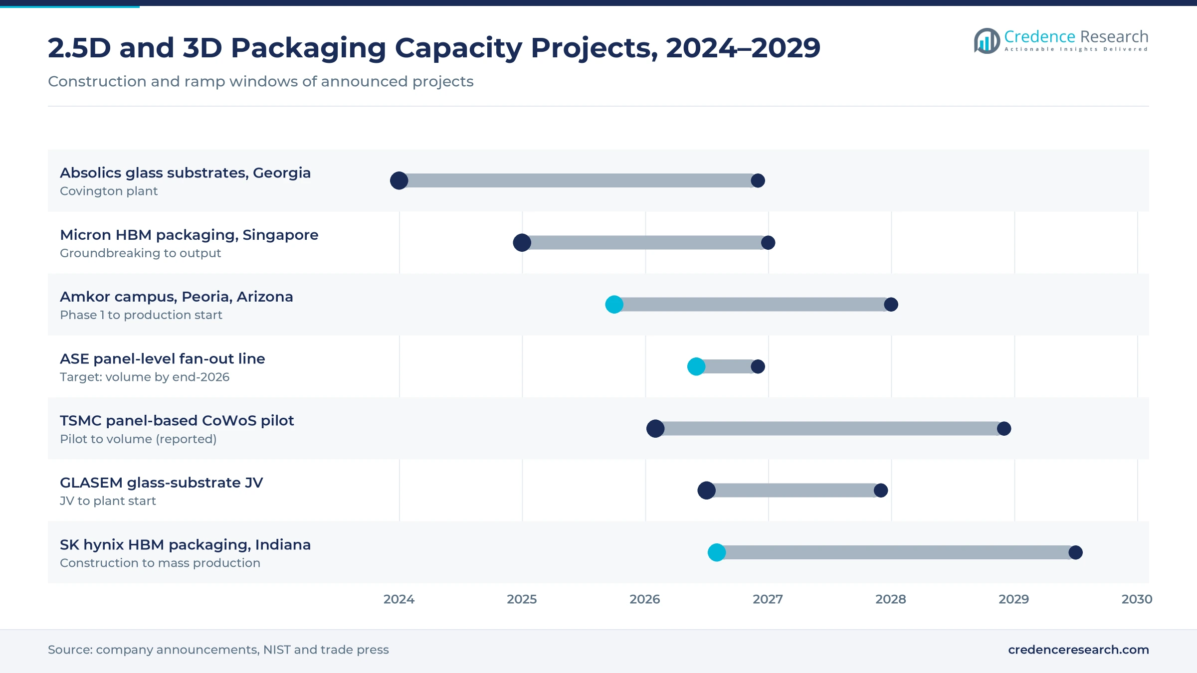
Foundry and OSAT investment in CoWoS-type interposers, TSV, hybrid bonding and fan-out capacity adds about 2.4 percentage points to the forecast CAGR. ASE spent USD 2.7 billion on machinery and USD 1.4 billion on facilities in the first half of 2026. Amkor broke ground on its Peoria, Arizona campus in October 2025, with Apple and NVIDIA named as customers. The US CHIPS National Advanced Packaging Manufacturing Program finalized USD 1.4 billion of awards in January 2025, as listed by NIST. The risk is overbuild if AI spending slows.
Hybrid Bonding, Panels, Glass and Optics Mark the Next Packaging Wave
Trend 1: Is hybrid bonding moving into volume?
Yes, for logic. Hybrid bonding, which joins copper pads directly without solder bumps, is in volume for stacked cache and some server processors. Hybrid bonding is the fastest-growing technology at 20.69% a year. Besi, the main tool supplier, reported second-quarter 2026 orders of EUR 292.9 million, up 128.8%, as stated in its Q2 2026 results. For HBM, memory makers kept thermo-compression bonding for HBM4 after JEDEC relaxed the stack height limit.
Trend 2: Are panels replacing wafers?
Partly. Panel-level fan-out processes rectangular panels instead of round wafers to fit larger packages. ASE targets mass production on its first automated panel line by the end of 2026, and TSMC is building a pilot line for panel-based CoWoS. Panel processes still face warpage and yield challenges.
Trend 3: When will glass substrates arrive?
Glass cores offer flatter, more stable substrates for very large packages. Glass is the fastest-growing substrate at 39.40% a year, but from a very small base, since no glass-core product was on the market in 2025. Samsung Electro-Mechanics and Dongwoo formed a glass-substrate joint venture in July 2026. More detail appears in the glass substrate market.
Trend 4: Is optics moving into the package?
NVIDIA announced co-packaged optics switches in March 2025, built with TSMC's packaging. RF and photonics is the fastest-growing application at 17.93% a year.
Capacity Bottlenecks, Yield and Thermal Limits Constrain Growth
Why is capacity still tight?
Interposer, HBM and substrate capacity takes two to three years to build. ASE has described hardware infrastructure as the bottleneck and lifted its capex. Customers that cannot secure capacity delay product launches, which shifts share toward suppliers that already have lines.
How do yields affect cost?
A 2.5D package joins several expensive dies, so one defect can scrap the whole assembly. Yields on large interposers and tall memory stacks remain below those of simple packages, which raises cost per good unit and limits adoption outside high-value products.
Why is heat a constraint?
Stacking dies traps heat. Thermal design limits how many layers and how much power a 3D stack can handle, which pushes designers toward liquid cooling and new materials.
Are new technologies arriving late?
Yes. Glass-core substrates were expected years earlier, and memory makers deferred hybrid bonding for HBM. Delays push some value to later in the forecast period.
Where are the opportunities?
Automotive and edge-AI chipmakers want chiplet packaging but lack the volume to reserve leading-edge capacity. OSATs that offer standard chiplet platforms on smaller interposers can serve them. The execution risk is qualification for automotive reliability standards, which takes years.
Asia Pacific Leads Packaging Value, While North America Builds Capacity
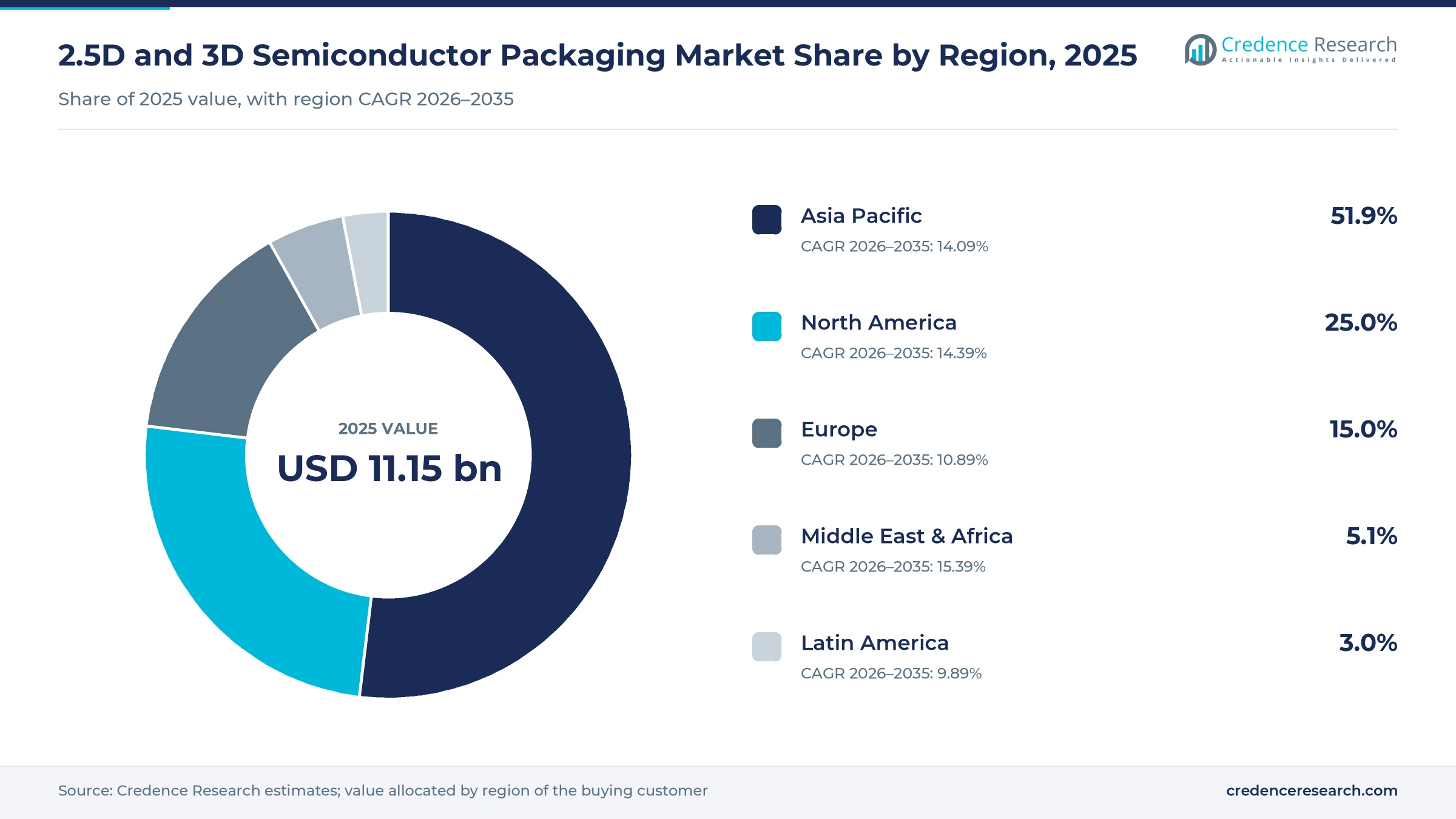
Value is allocated by the region of the customer that buys the packaged device.
| Region | Share 2025 | CAGR 2026–2035 |
|---|---|---|
| Asia Pacific | 51.9% | 14.09% |
| North America | 25.0% | 14.39% |
| Europe | 15.0% | 10.89% |
| Middle East & Africa | 5.1% | 15.39% |
| Latin America | 3.0% | 9.89% |
Why does Asia Pacific lead?
Asia Pacific holds a 51.9% share in 2025 and grows at 14.09% a year. Taiwan, South Korea, China and Japan host the main foundries, memory makers and OSATs, and many device makers in the region buy advanced packages for phones, PCs and servers. China's OSATs are adding capacity for domestic AI chips.
What drives North America?
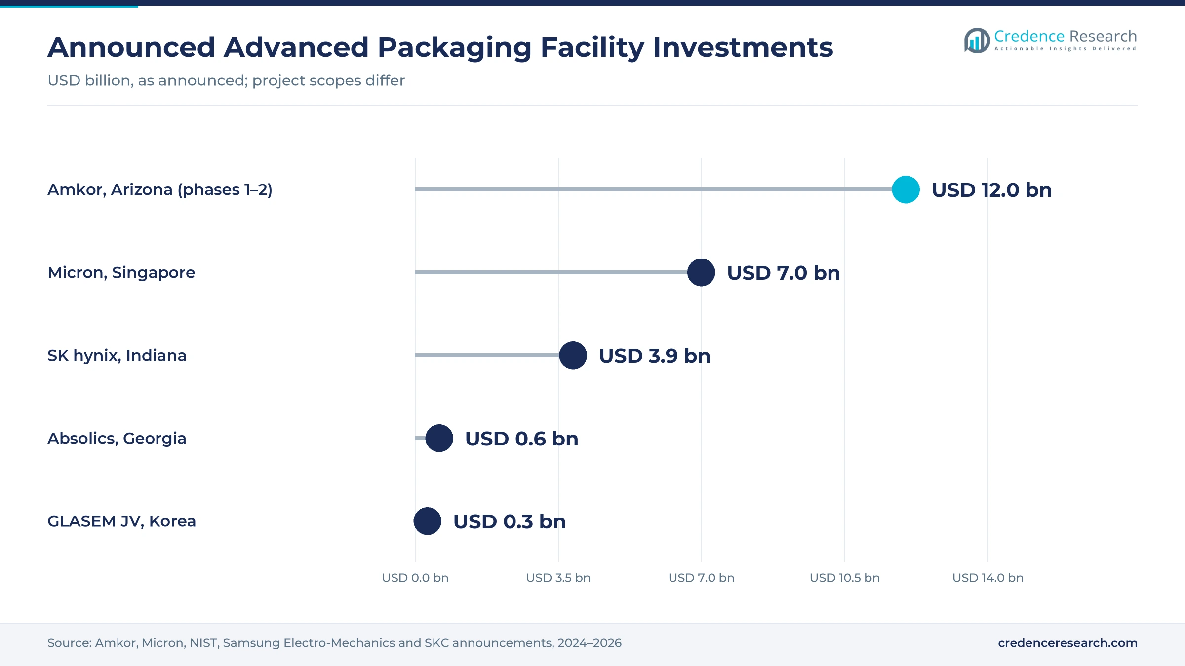
North America holds 25.0% and grows at 14.39% a year. US chip designers and cloud providers buy most AI accelerators, and the region is adding packaging capacity through Amkor in Arizona, SK hynix in Indiana and Absolics in Georgia.
What shapes Europe?
Europe holds 15.0% and grows at 10.89% a year. Automotive, industrial and telecom chipmakers buy advanced packages, and the region supplies key equipment such as hybrid-bonding tools.
What about Latin America and the Middle East & Africa?
Latin America holds 3.0% and grows at 9.89%, mainly through electronics assembly in Mexico and Brazil. The Middle East & Africa region holds 5.1% and is the fastest-growing region at 15.39% a year, as Gulf states build AI data centers that use accelerators with 2.5D packaging.
Plant Investments, Funding and Technology Launches, 2025–2026
| Development | Status and why it matters |
|---|---|
| In August 2026, SK hynix broke ground on an HBM packaging plant of more than USD 4 billion in West Lafayette, Indiana. | Under construction. Adds US HBM packaging capacity. |
| In July 2026, ASE announced in a Form 6-K that its leading-edge advanced packaging revenue was tracking ahead of USD 3.5 billion for 2026. | Reported. Confirms rapid growth in OSAT advanced packaging. |
| In July 2026, Besi announced second-quarter orders of EUR 292.9 million, up 128.8%, led by hybrid bonding. | Reported. Signals hybrid-bonding adoption. |
| In July 2026, SEMI announced a forecast of USD 6.7 billion in assembly and packaging equipment sales for 2026, rising to USD 8.6 billion in 2028. | Published. Shows continued capacity investment. |
| In July 2026, Samsung Electro-Mechanics and Dongwoo signed an agreement to form the GLASEM glass-substrate joint venture. | Announced. Prepares glass-core supply. |
| In June 2026, TSMC and Amkor signed a 10-year agreement for advanced packaging and test services in Arizona. | Signed. Anchors US packaging capacity. |
| In October 2025, Amkor broke ground on its Peoria, Arizona campus and raised the planned investment to USD 7 billion. | Under construction. Largest US advanced packaging site. |
| In August 2025, the UCIe Consortium launched its 3.0 specification at 64 GT/s. | Released. Supports chiplet interoperability. |
| In January 2025, the US Department of Commerce announced USD 1.4 billion in final awards under the National Advanced Packaging Manufacturing Program. | Awarded. Funds glass, silicon-core and panel packaging research. |
Need a Custom Version of This Report?
Tailor the scope, geography, or segments to your exact requirements.
- Custom geography or segment scope
- Direct access to our analyst team
Foundries, OSATs and Memory Makers Share the Advanced Package
Three kinds of supplier compete, and they often cooperate on the same product. Because few suppliers report 2.5D and 3D revenue separately, no share ranking is given.
What role do foundries play?
Taiwan Semiconductor Manufacturing Co. (TSMC) leads in high-end 2.5D through its CoWoS family and in 3D stacking through SoIC. It controls the most advanced interposer capacity and packages many of the world's AI accelerators. Intel Corporation offers EMIB bridges and Foveros stacking for its own products and for foundry customers. Samsung Electronics offers foundry packaging and is also a major HBM supplier.
What role do OSATs play?
ASE Technology Holding, including its SPIL subsidiary, is the largest outsourced packaging firm and is expanding leading-edge capacity and panel lines. Amkor Technology runs plants in Asia and is building the largest US advanced packaging campus. JCET Group, China's largest OSAT, offers chiplet integration platforms for domestic customers.
What role do memory makers play?
SK hynix, Samsung Electronics and Micron Technology stack DRAM dies with through-silicon vias to make HBM, and their HBM capacity sets how many accelerators can be built. Micron broke ground on an HBM packaging plant in Singapore in January 2025, and SK hynix is building one in Indiana.
How do they compete?
Suppliers compete on capacity, yield, interconnect density and the ability to co-design with chip customers. Long-term agreements, such as the June 2026 deal for TSMC to buy US packaging services from Amkor, lock in partnerships. Related designs are covered in the 3D IC and 2.5D IC packaging market.
Frequently Asked Questions
How big is the 2.5D and 3D semiconductor packaging market?
What is driving demand for 2.5D and 3D packaging?
Which packaging technology grows fastest?
Which region leads the market?
Who are the main suppliers?
Why do glass substrates matter?
Table of Content
Chapter 1 Market Segmentation
- 1.1 Segmentation Framework
- 1.1.1 Product and Service Classification
- 1.1.2 Application and End-Use Classification
- 1.1.3 Technology and Solution Classification
- 1.1.4 Customer and Distribution Channel Classification
- 1.1.5 Geographic Segmentation
- 1.1.6 Market Segment Definitions and Boundaries
- 1.2 By Packaging Technology
- 1.2.1 2.5D Interposer/Fan-Out on Substrate
- 1.2.2 3D TSV
- 1.2.3 Hybrid Bonding
- 1.2.4 Panel-Level Fan-Out
- 1.3 By Application
- 1.3.1 Memory/HBM
- 1.3.2 Logic/Processors
- 1.3.3 RF/Photonics
- 1.3.4 Image Sensors
- 1.3.5 MEMS
- 1.4 By Substrate
- 1.4.1 Organic Build-Up
- 1.4.2 Silicon Interposer
- 1.4.3 Glass Core
- 1.4.4 Ceramic
- 1.5 By End Use
- 1.5.1 AI/Data Center
- 1.5.2 Consumer Electronics
- 1.5.3 Automotive/ADAS
- 1.5.4 Telecom
- 1.5.5 Aerospace & Defense
- 1.6 By Integration
- 1.6.1 Chiplets
- 1.6.2 Die-to-Wafer
- 1.6.3 Wafer-to-Wafer
- 1.6.4 Package-on-Package
- 1.7 By Provider Type
- 1.7.1 Foundry
- 1.7.2 OSAT
- 1.7.3 IDM
Chapter 2 Introduction
- 2.1 Report Objectives and Scope
- 2.2 Product Definition and Industry Terminology
- 2.3 Market Inclusions and Exclusions
- 2.4 Research Process
- 2.4.1 Primary Research and Expert Interviews
- 2.4.2 Secondary Research and Source Review
- 2.4.3 Top-Down and Bottom-Up Estimation
- 2.4.4 Data Triangulation and Verification
- 2.5 Market Size Measurement Basis
- 2.5.1 2025: USD 11.15 billion → 2035: USD 40.40 billion
- 2.6 Historical and Forecast Reference Periods
- 2.6.1 Historical Period: 2018-2025
- 2.6.2 Base Year: 2025
- 2.6.3 Forecast Period: 2025-2035
- 2.7 Research Assumptions and Limitations
Chapter 3 Executive Summary
- 3.1 Market Snapshot and Key Findings
- 3.2 Base-Year Market Size, 2025
- 3.3 Forecast Market Size, 2035
- 3.4 Revenue and Volume Growth Outlook
- 3.5 Key Demand and Supply Indicators
- 3.6 Leading Market Segments
- 3.7 Fastest-Growing Market Opportunities
- 3.8 Regional Performance Highlights
- 3.9 Technology and Industry Transformation
- 3.10 Competitive Landscape Summary
- 3.11 Analyst View and Strategic Implications
Chapter 4 Global 2.5D and 3D Semiconductor Packaging Market Trends and Developments
- 4.1 Historical Industry Development, 2018-2025
- 4.2 Recent Market Trends and Developments
- 4.3 Demand and Customer Behavior Trends
- 4.4 Technology and Product Innovation
- 4.5 Artificial Intelligence, Automation and Digitalization
- 4.6 Local Manufacturing and Supply Chain Realignment
- 4.7 Industry Partnerships, Mergers and Acquisitions
- 4.8 Sustainability and Circular Economy Developments
- 4.9 Government and Private Sector Investment Trends
- 4.10 Emerging Business Models and Commercialization
- 4.11 Industry Developments and Announcements
Chapter 5 Global 2.5D and 3D Semiconductor Packaging Market Production, Supply and Demand Analysis
- 5.1 Demand Trend and Consumption Analysis, 2018-2025
- 5.2 Demand Forecast, 2025-2035
- 5.3 Production and Output Trend, 2018-2025
- 5.4 Production and Output Forecast, 2025-2035
- 5.5 Installed Capacity and Capacity Utilization
- 5.6 Company-Wise Production Plants and Statistics
- 5.6.1 Installed Production Capacity
- 5.6.2 Actual Production
- 5.6.3 Planned Capacity and Expansion Targets
- 5.7 Supply Chain Structure and Procurement Trends
- 5.8 Supply-Demand Gap and Bottlenecks
- 5.9 Import Dependence and Sourcing Structure
- 5.10 Contract Manufacturing and Outsourcing
- 5.11 Regional Supply and Demand Concentration
Chapter 6 Global 2.5D and 3D Semiconductor Packaging Market Pricing Analysis
- 6.1 Pricing Structure and Measurement
- 6.2 Historical Pricing Trends, 2018-2025
- 6.3 Pricing Outlook, 2025-2035
- 6.4 Average Selling Price and Unit Economics
- 6.5 Pricing by Product and Market Segment
- 6.6 Geographic Pricing Differences
- 6.7 Key Input, Energy, Labor and Logistics Costs
- 6.8 Contract Pricing and Purchasing Models
- 6.9 Pricing Sensitivity and Competitive Positioning
- 6.10 Price, Margin and Profitability Implications
Chapter 7 Global 2.5D and 3D Semiconductor Packaging Market Dynamics
- 7.1 Market Growth Drivers
- 7.1.1 Demand-Side Drivers
- 7.1.2 Technology and Innovation Drivers
- 7.1.3 Infrastructure and Investment Drivers
- 7.1.4 Regulatory and Policy Drivers
- 7.2 Market Restraints
- 7.2.1 Cost and Affordability Constraints
- 7.2.2 Technology and Adoption Barriers
- 7.2.3 Supply Chain and Operational Constraints
- 7.3 Market Challenges
- 7.3.1 Competitive Pressure and Margin Erosion
- 7.3.2 Skills, Infrastructure and Implementation Gaps
- 7.4 Emerging Market Opportunities
- 7.5 Market Dynamics Impact and Time-Horizon Assessment
Chapter 8 Global 2.5D and 3D Semiconductor Packaging Value Chain Analysis
- 8.1 Industry Value Chain Overview
- 8.2 Upstream Suppliers and Critical Inputs
- 8.3 Technology and Component Providers
- 8.4 Manufacturing or Service Delivery
- 8.5 Distribution, Channel Partners and Integrators
- 8.6 Downstream Applications and End Users
- 8.7 Value Addition and Profit Pools
- 8.8 Vertical Integration and Outsourcing
- 8.9 Supplier Concentration and Risk
- 8.10 Supply Chain Localization and Resilience
Chapter 9 Global 2.5D and 3D Semiconductor Packaging Market Regulations and Policies
- 9.1 Relevant Laws, Standards and Compliance Frameworks
- 9.2 Product, Service, Safety and Quality Requirements
- 9.3 Government Policies, Incentives and Subsidies
- 9.4 Imports, Exports and Trade Barriers
- 9.5 Public Procurement and Local Content Requirements
- 9.6 Environmental and Sustainability Compliance
- 9.7 Upcoming Policy Changes and Market Implications
Chapter 10 Global 2.5D and 3D Semiconductor Packaging Market Hotspots and Opportunities
- 10.1 Market Opportunity Mapping and Growth Hotspots
- 10.2 High-Growth Applications and Customer Groups
- 10.3 Underserved Markets and White-Space Opportunities
- 10.4 Emerging Technology and Product Opportunities
- 10.5 New Capacity and Investment Hotspots
- 10.6 Market Entry and Expansion Opportunities
- 10.7 Distribution and Partnership Opportunities
- 10.8 Near-Term and Long-Term Commercial Potential
- 10.9 Opportunity Attractiveness and Execution Risks
Chapter 11 Global 2.5D and 3D Semiconductor Packaging Market Outlook, 2025-2035
- 11.1 Market Size and Analysis
- 11.1.1 Revenue (Market Measurement: 2025: USD 11.15 billion → 2035: USD 40.40 billion)
- 11.1.2 Market Volume and Quantity Sold
- 11.1.3 Historical Market Size, 2018-2025
- 11.1.4 Base-Year Market Size, 2025
- 11.2 Market Forecast, 2025-2035
- 11.2.1 Revenue Forecast to 2035
- 11.2.2 Volume Forecast to 2035
- 11.2.3 CAGR and Year-on-Year Growth
- 11.2.4 Incremental Revenue Opportunity
- 11.3 Forecast Assumptions and Scenario Analysis
- 11.3.1 Base-Case Forecast
- 11.3.2 Optimistic and Conservative Scenarios
- 11.3.3 Technology, Pricing and Policy Sensitivities
- 11.4 Market Attractiveness and Growth Outlook
Chapter 12 Global 2.5D and 3D Semiconductor Packaging Market Segmentation and Outlook
- 12.1 Segmentation Summary and Market Shares, 2025
- 12.2 Largest and Fastest-Growing Segments
- 12.3 By Packaging Technology - Market Size and Forecast, 2025-2035
- 12.3.1 Segment Definition and Scope
- 12.3.2 Historical Market Size, 2018-2025
- 12.3.3 Revenue Forecast, 2025-2035
- 12.3.4 Volume Forecast, 2025-2035
- 12.3.5 Base-Year Market Share, 2025
- 12.3.6 Segment CAGR and Growth Drivers
- 12.3.7 Subsegment Market Size and Forecast
- 12.3.7.1 2.5D Interposer/Fan-Out on Substrate
- 12.3.7.2 3D TSV
- 12.3.7.3 Hybrid Bonding
- 12.3.7.4 Panel-Level Fan-Out
- 12.3.8 Subsegment Pricing and Adoption Trends
- 12.3.9 Leading Suppliers and Competition
- 12.3.10 Regional Demand and Opportunities
- 12.4 By Application - Market Size and Forecast, 2025-2035
- 12.4.1 Segment Definition and Scope
- 12.4.2 Historical Market Size, 2018-2025
- 12.4.3 Revenue Forecast, 2025-2035
- 12.4.4 Volume Forecast, 2025-2035
- 12.4.5 Base-Year Market Share, 2025
- 12.4.6 Segment CAGR and Growth Drivers
- 12.4.7 Subsegment Market Size and Forecast
- 12.4.7.1 Memory/HBM
- 12.4.7.2 Logic/Processors
- 12.4.7.3 RF/Photonics
- 12.4.7.4 Image Sensors
- 12.4.7.5 MEMS
- 12.4.8 Subsegment Pricing and Adoption Trends
- 12.4.9 Leading Suppliers and Competition
- 12.4.10 Regional Demand and Opportunities
- 12.5 By Substrate - Market Size and Forecast, 2025-2035
- 12.5.1 Segment Definition and Scope
- 12.5.2 Historical Market Size, 2018-2025
- 12.5.3 Revenue Forecast, 2025-2035
- 12.5.4 Volume Forecast, 2025-2035
- 12.5.5 Base-Year Market Share, 2025
- 12.5.6 Segment CAGR and Growth Drivers
- 12.5.7 Subsegment Market Size and Forecast
- 12.5.7.1 Organic Build-Up
- 12.5.7.2 Silicon Interposer
- 12.5.7.3 Glass Core
- 12.5.7.4 Ceramic
- 12.5.8 Subsegment Pricing and Adoption Trends
- 12.5.9 Leading Suppliers and Competition
- 12.5.10 Regional Demand and Opportunities
- 12.6 By End Use - Market Size and Forecast, 2025-2035
- 12.6.1 Segment Definition and Scope
- 12.6.2 Historical Market Size, 2018-2025
- 12.6.3 Revenue Forecast, 2025-2035
- 12.6.4 Volume Forecast, 2025-2035
- 12.6.5 Base-Year Market Share, 2025
- 12.6.6 Segment CAGR and Growth Drivers
- 12.6.7 Subsegment Market Size and Forecast
- 12.6.7.1 AI/Data Center
- 12.6.7.2 Consumer Electronics
- 12.6.7.3 Automotive/ADAS
- 12.6.7.4 Telecom
- 12.6.7.5 Aerospace & Defense
- 12.6.8 Subsegment Pricing and Adoption Trends
- 12.6.9 Leading Suppliers and Competition
- 12.6.10 Regional Demand and Opportunities
- 12.7 By Integration - Market Size and Forecast, 2025-2035
- 12.7.1 Segment Definition and Scope
- 12.7.2 Historical Market Size, 2018-2025
- 12.7.3 Revenue Forecast, 2025-2035
- 12.7.4 Volume Forecast, 2025-2035
- 12.7.5 Base-Year Market Share, 2025
- 12.7.6 Segment CAGR and Growth Drivers
- 12.7.7 Subsegment Market Size and Forecast
- 12.7.7.1 Chiplets
- 12.7.7.2 Die-to-Wafer
- 12.7.7.3 Wafer-to-Wafer
- 12.7.7.4 Package-on-Package
- 12.7.8 Subsegment Pricing and Adoption Trends
- 12.7.9 Leading Suppliers and Competition
- 12.7.10 Regional Demand and Opportunities
- 12.8 By Provider Type - Market Size and Forecast, 2025-2035
- 12.8.1 Segment Definition and Scope
- 12.8.2 Historical Market Size, 2018-2025
- 12.8.3 Revenue Forecast, 2025-2035
- 12.8.4 Volume Forecast, 2025-2035
- 12.8.5 Base-Year Market Share, 2025
- 12.8.6 Segment CAGR and Growth Drivers
- 12.8.7 Subsegment Market Size and Forecast
- 12.8.7.1 Foundry
- 12.8.7.2 OSAT
- 12.8.7.3 IDM
- 12.8.8 Subsegment Pricing and Adoption Trends
- 12.8.9 Leading Suppliers and Competition
- 12.8.10 Regional Demand and Opportunities
- 12.9 Segment Growth Comparison
- 12.10 Segment Attractiveness and Priority Matrix
Chapter 13 Global 2.5D and 3D Semiconductor Packaging End-Use and Application Market Outlook
- 13.1 End-Use Industry and Customer Demand Structure
- 13.2 Leading Applications and Customer Groups
- 13.3 End-Use Market Size, Share and Forecast
- 13.4 Major End-Use Industry Deep Dives
- 13.4.1 Customer Requirements and Use Cases
- 13.4.2 Demand and Replacement Cycles
- 13.4.3 Technical and Regulatory Considerations
- 13.4.4 Purchasing and Procurement Models
- 13.4.5 Leading Vendors and Distribution Channels
- 13.4.6 Forecast and Commercial Opportunities
- 13.5 Emerging Applications and Cross-Segment Demand
- 13.6 End-Use Industry Investment Priorities
Chapter 14 Global 2.5D and 3D Semiconductor Packaging Geographic Market Outlook, 2025-2035
- 14.1 Regional Market Size and Share, 2025
- 14.2 Regional Market Forecast, 2025-2035
- 14.3 Regional Pricing, Production and Demand Differences
- 14.4 North America
- 14.4.1 United States
- 14.4.2 Canada
- 14.4.3 Mexico
- 14.5 Europe
- 14.5.1 Germany
- 14.5.2 France
- 14.5.3 Italy
- 14.5.4 United Kingdom
- 14.5.5 Spain
- 14.5.6 Poland
- 14.5.7 Russia
- 14.5.8 Netherlands
- 14.5.9 Belgium
- 14.5.10 Sweden
- 14.5.11 Denmark
- 14.5.12 Norway
- 14.5.13 Rest of Europe
- 14.6 Asia Pacific
- 14.6.1 China
- 14.6.2 India
- 14.6.3 Japan
- 14.6.4 South Korea
- 14.6.5 Thailand
- 14.6.6 Indonesia
- 14.6.7 Vietnam
- 14.6.8 Malaysia
- 14.6.9 Australia
- 14.6.10 Rest of Asia Pacific
- 14.7 Latin America
- 14.7.1 Brazil
- 14.7.2 Argentina
- 14.7.3 Colombia
- 14.7.4 Chile
- 14.7.5 Rest of Latin America
- 14.8 Middle East
- 14.8.1 Saudi Arabia
- 14.8.2 United Arab Emirates
- 14.8.3 Turkey
- 14.8.4 Israel
- 14.8.5 Iran
- 14.8.6 Rest of the Middle East
- 14.9 Africa
- 14.9.1 South Africa
- 14.9.2 Egypt
- 14.9.3 Nigeria
- 14.9.4 Morocco
- 14.9.5 Rest of Africa
- 14.10 Regional Investment, Policy and Supply Chain Differences
- 14.11 Regional Competitive Landscape
- 14.12 Geographic Growth Hotspots
Chapter 15 Global 2.5D and 3D Semiconductor Packaging Technology, Innovation and Sustainability Outlook
- 15.1 Technology Landscape and Maturity
- 15.2 Product, Process and Service Innovation
- 15.3 AI, Automation and Digital Tools in the Industry
- 15.4 Technology Adoption and Performance Benchmarking
- 15.5 Innovation Pipeline and R&D Investment
- 15.6 Patent and Intellectual Property Trends
- 15.7 Energy Efficiency and Resource Management
- 15.8 Sustainability, Recycling and Circularity
- 15.9 Technology Roadmap, 2025-2035
- 15.10 Risks of Obsolescence and Technology Substitution
Chapter 16 Global 2.5D and 3D Semiconductor Packaging Market Key Strategic Imperatives
- 16.1 Growth and Market Entry Priorities
- 16.2 High-Return Products and Segments
- 16.3 Pricing, Profitability and Cost Optimization
- 16.4 Technology Investment and Product Differentiation
- 16.5 Supply Chain Localization and Resilience
- 16.6 Distribution and Customer Acquisition
- 16.7 Partnership, Acquisition and Capacity Strategy
- 16.8 Regional Expansion Priorities
- 16.9 Short-, Medium- and Long-Term Actions
Chapter 17 Competition Outlook
- 17.1 Industry Competition Characteristics
- 17.2 Market Structure and Concentration
- 17.3 Market Share and Competitive Positioning, 2025
- 17.4 Company-Wise Revenue and Product Benchmarking
- 17.5 Production and Service Capacity Benchmarking
- 17.6 Technology, Pricing and Differentiation
- 17.7 Regional Footprint and Distribution Strength
- 17.8 Mergers, Acquisitions and Strategic Alliances
- 17.9 New Entrants and Competitive Threats
- 17.10 Porter's Five Forces and Industry Attractiveness
- 17.11 Competitive Outlook, 2025-2035
Chapter 18 Company Profiles
- 18.1 Company Coverage and Selection Criteria
- 18.2 Taiwan Semiconductor Manufacturing Co.
- 18.2.1 Business Description
- 18.2.2 Company Ownership and Geographic Presence
- 18.2.3 Product and Service Portfolio
- 18.2.4 Manufacturing and Operating Footprint
- 18.2.5 Production Capacity and Expansion Plans
- 18.2.6 Financial Performance and Investment
- 18.2.7 Market Share and Competitive Position
- 18.2.8 Technology and Innovation Capabilities
- 18.2.9 Strategic Alliances or Partnerships
- 18.2.10 Recent Developments
- 18.2.11 Growth Strategy and Outlook
- 18.3 Samsung Electronics
- 18.4 Intel Corporation
- 18.5 ASE Technology Holding
- 18.6 Amkor Technology
- 18.7 JCET Group
- 18.8 SK hynix
- 18.9 Micron Technology
- 18.10 Other Relevant Market Participants
Note: Every listed company is profiled on the structure shown under the first company. The company list is preliminary and may change based on research findings, market developments, data availability and client requirements.
Chapter 19 Disclaimer
- 19.1 Research and Forecast Disclaimer
- 19.2 Data Source and Estimation Limitations
Note: The depth of individual sections depends on data availability for this market. Volume, capacity, trade and other unit-based metrics are included where applicable.