Market Overview
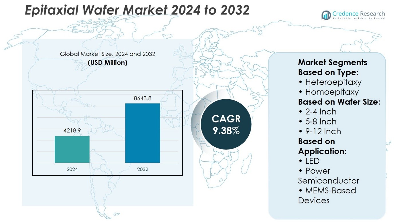
Epitaxial Wafer Market size was valued at USD 4218.9 million in 2024 and is anticipated to reach USD 8643.8 million by 2032, at a CAGR of 9.38% during the forecast period.
| REPORT ATTRIBUTE |
DETAILS |
| Historical Period |
2020-2024 |
| Base Year |
2024 |
| Forecast Period |
2025-2032 |
| Epitaxial Wafer Market Size 2024 |
USD 4218.9 Million |
| Epitaxial Wafer Market, CAGR |
9.38% |
| Epitaxial Wafer Market Size 2032 |
USD 8643.8 Million |
The Epitaxial Wafer Market is driven by advancements in compound semiconductor materials such as GaN, SiC, and InP, which offer superior performance in high-frequency, high-power, and optoelectronic applications. Rising demand from automotive electrification, 5G infrastructure, and LED manufacturing accelerates adoption of high-quality wafers with precise doping and low defect density. It benefits from the shift toward larger wafer diameters, improving production efficiency and reducing costs. Integration of advanced metrology, AI-driven process control, and customized wafer designs enhances quality and application-specific performance. Growing investment in wide-bandgap semiconductor capacity further strengthens its position in power electronics, photonics, and high-speed communication markets.
The Epitaxial Wafer Market is geographically led by Asia-Pacific with 41% share, followed by North America at 27% and Europe at 22%, while Latin America and the Middle East & Africa each hold 5%. Asia-Pacific dominates due to extensive semiconductor fabrication capacity and strong demand from electronics and communication sectors. Key players include IntelliEPI, Silicon Valley Microelectronics Inc., IQE PLC, Showa Denko K. K., GlobalWafers, Epistar Corporation, Jenoptic AG, II-VI Incorporated, Nichia Corporation, and Electronics And Materials Corporation Limited.
Access crucial information at unmatched prices!
Request your sample report today & start making informed decisions powered by Credence Research Inc.!
Download Sample
Market Insights
- The Epitaxial Wafer Market was valued at USD 4,218.9 million in 2024 and is projected to reach USD 8,643.8 million by 2032, growing at a CAGR of 9.38%.
- Advancements in GaN, SiC, and InP materials drive superior performance in high-frequency, high-power, and optoelectronic devices.
- Rising demand from electric vehicles, 5G infrastructure, and LED manufacturing accelerates adoption of high-quality epitaxial wafers.
- Leading players focus on wide-bandgap materials, larger wafer diameters, and AI-driven process control for improved yield and cost efficiency.
- High production costs, complex manufacturing processes, and supply chain constraints for specialty substrates pose market challenges.
- Asia-Pacific leads with 41% share, followed by North America at 27% and Europe at 22%, with other regions sharing the remainder.
- Key companies include IntelliEPI, Silicon Valley Microelectronics Inc., IQE PLC, Showa Denko K. K., GlobalWafers, Epistar Corporation, Jenoptic AG, II-VI Incorporated, Nichia Corporation, and Electronics And Materials Corporation Limited.
Market Drivers
Advancements in Compound Semiconductor Technologies
The Epitaxial Wafer Market benefits from rapid innovation in compound semiconductor materials such as gallium arsenide (GaAs), gallium nitride (GaN), and indium phosphide (InP). These materials enable superior electron mobility, higher breakdown voltages, and better thermal stability than traditional silicon. Manufacturers deploy advanced metal-organic chemical vapor deposition (MOCVD) and molecular beam epitaxy (MBE) systems to achieve precise layer thickness and uniformity. It supports applications in high-frequency communication, power electronics, and photonics with enhanced performance metrics. Growing integration of GaN in 5G base stations and electric vehicle power modules further strengthens market demand. Continuous research into lattice-matched substrates enhances efficiency and reduces defect density.
- For instance, IQE PLC reported the production of over 150 million square centimeters of GaN epitaxial wafers enabling high-performance power and RF device manufacturing with reduced defect densities.
Rising Demand from Consumer Electronics Sector
Consumer electronics drive a significant portion of demand for epitaxial wafers, particularly in optoelectronic devices. The Epitaxial Wafer Market sees strong uptake in LEDs, laser diodes, and photodetectors for smartphones, wearables, and augmented reality devices. It supports compact designs while improving brightness, energy efficiency, and durability. Manufacturers optimize wafer structures to meet the stringent reliability requirements of portable devices. Growing adoption of micro-LED displays and advanced camera sensors increases the need for high-quality epitaxial layers. Companies expand production capacity to meet the scaling requirements of global electronics brands.
- For instance, Nichia Corporation produced approximately 500 million LED epitaxial wafers focusing on high-brightness LEDs with luminous efficacy exceeding 200 lumens per watt, supporting next-generation display and lighting technologies.
Expanding Role in Automotive and Power Applications
Automotive electrification significantly boosts the demand for high-performance epitaxial wafers. The Epitaxial Wafer Market supports silicon carbide (SiC) and GaN-based devices that operate efficiently at high voltages and temperatures. It enables longer driving ranges, faster charging times, and improved power conversion efficiency in electric vehicles. Wide-bandgap semiconductor wafers also enhance performance in advanced driver-assistance systems (ADAS) and onboard charging systems. Increasing government regulations on vehicle emissions accelerate the shift toward these technologies. Leading suppliers invest in larger wafer diameters to improve cost efficiency and throughput.
Growth in Data and Communication Infrastructure
The expansion of data centers and high-speed communication networks directly supports demand for epitaxial wafers. The Epitaxial Wafer Market supplies critical substrates for optical transceivers, high-frequency RF devices, and satellite communication systems. It enables higher bandwidth, lower latency, and greater energy efficiency in network infrastructure. The growth of 5G, cloud computing, and IoT ecosystems increases the requirement for wafers with precise doping profiles and defect control. Manufacturers collaborate with telecom equipment providers to customize wafer properties for specific performance goals. Emerging 6G research programs are expected to accelerate long-term demand for advanced epitaxial technologies.
Market Trends
Shift Toward Larger Wafer Diameters
The Epitaxial Wafer Market is witnessing a transition from smaller diameters to 6-inch and 8-inch wafers for compound semiconductor production. Larger diameters improve manufacturing throughput and reduce cost per device. It supports scalability for high-volume applications such as automotive power electronics and data center components. Equipment vendors adapt MOCVD and MBE platforms to handle these larger substrates without compromising crystal quality. This shift aligns with demand for higher yields and tighter process control in advanced semiconductor fabs. Manufacturers invest in capacity expansion to meet long-term supply requirements.
- For instance, Epistar Corporation reported manufacturing 12 million 6-inch GaN epitaxial wafers in primarily for LED and power device applications, maintaining stringent quality control for enhanced device performance.
Rising Adoption of Gallium Nitride and Silicon Carbide Materials
Demand for GaN and SiC epitaxial wafers continues to expand across high-performance power and RF applications. The Epitaxial Wafer Market benefits from the superior efficiency, high breakdown voltage, and thermal stability of these materials. It enables improved performance in electric vehicles, renewable energy systems, and 5G base stations. Suppliers enhance wafer surface quality and reduce defect densities to meet stringent device specifications. GaN-on-silicon and SiC-on-SiC structures are gaining traction due to improved manufacturing economics. This trend is reinforced by government-backed programs promoting wide-bandgap semiconductor adoption.
- For instance, II-VI Incorporated produced 7.5 million 4-inch SiC epitaxial wafers in designed for electric vehicle power modules and 5G RF components, demonstrating advanced uniformity and low defect densities critical for device reliability.
Integration of Advanced Metrology and Inspection Tools
Quality assurance in epitaxial wafer manufacturing is becoming more sophisticated through in-line metrology and defect detection systems. The Epitaxial Wafer Market adopts optical, X-ray, and electron-based inspection techniques for real-time process monitoring. It allows manufacturers to detect sub-micron defects and optimize growth conditions. Automated feedback loops in MOCVD reactors improve uniformity and doping precision across the wafer surface. Adoption of AI-assisted analytics helps in predictive maintenance and yield enhancement. This integration reduces rework rates and strengthens supplier competitiveness.
Growth in Custom and Application-Specific Wafer Designs
End-users are requesting wafers tailored for specific device architectures and performance targets. The Epitaxial Wafer Market meets this demand by offering customized doping profiles, layer thicknesses, and substrate orientations. It supports specialized applications in photonics, quantum computing, and high-frequency radar systems. Manufacturers work closely with device designers to align wafer properties with system-level requirements. Hybrid structures combining multiple semiconductor materials are gaining attention for multifunctional integration. This trend drives collaborative R&D between wafer suppliers and end-device manufacturers.
Market Challenges Analysis
High Production Costs and Complex Manufacturing Processes
The Epitaxial Wafer Market faces significant challenges in balancing production costs with quality requirements. Epitaxial growth methods such as MOCVD and MBE demand high-precision equipment, costly precursors, and extensive process control. It requires maintaining ultra-clean environments to achieve low defect densities, which increases operational expenses. Scaling to larger wafer diameters further complicates uniformity control, often leading to yield losses if parameters are not tightly managed. The limited availability of skilled technicians for advanced epitaxy processes also constrains throughput. Rising energy costs and the need for constant reactor operation intensify the financial burden on manufacturers.
Supply Chain Constraints and Material Quality Issues
Securing reliable access to high-purity substrates and specialty gases remains a persistent challenge. The Epitaxial Wafer Market depends on stable supply chains for silicon carbide, gallium nitride, and indium phosphide substrates, many of which have limited global suppliers. It is vulnerable to disruptions that can delay production schedules and impact customer deliveries. Variations in substrate quality can lead to higher defect rates and reduced device performance, demanding rigorous incoming inspection protocols. Long lead times for advanced MOCVD reactors and spare parts hinder capacity expansion plans. Fluctuating raw material availability also drives pricing volatility, affecting long-term contract stability between wafer producers and end-users.
Market Opportunities
Expansion in Wide-Bandgap Semiconductor Applications
The Epitaxial Wafer Market has significant growth potential in applications leveraging wide-bandgap materials such as GaN and SiC. These materials offer superior efficiency, higher power density, and better thermal management, creating opportunities in electric vehicles, renewable energy systems, and industrial power conversion. It enables device miniaturization while improving performance under high-voltage and high-temperature conditions. Growing adoption of SiC MOSFETs and GaN HEMTs in automotive and telecom sectors supports demand for high-quality epitaxial wafers. Manufacturers that invest in larger wafer diameters and improved crystal quality can capture a larger share of these expanding markets. Collaborative R&D with device makers accelerates innovation and strengthens competitive positioning.
Rising Demand from Emerging Technology Segments
Emerging applications in quantum computing, photonics, and advanced radar systems open new revenue streams for epitaxial wafer suppliers. The Epitaxial Wafer Market can address these needs through customized doping profiles, heterostructures, and novel substrate combinations. It supports integration of multiple functionalities on a single wafer, enabling next-generation device architectures. Rapid development in LiDAR for autonomous vehicles and high-speed optical communication further drives specialized wafer requirements. Suppliers capable of meeting stringent reliability and performance metrics will gain strategic advantages. Investment in application-specific product lines and advanced metrology tools positions manufacturers to serve these high-value technology segments effectively.
Market Segmentation Analysis:
By Type
The Epitaxial Wafer Market is divided into heteroepitaxy and homoepitaxy based on the relationship between the substrate and the epitaxial layer. Heteroepitaxy involves depositing a crystalline layer on a substrate with a different lattice structure, enabling the use of materials such as GaN on silicon for cost-effective, high-performance devices. It supports applications in LEDs, high-frequency RF components, and power semiconductors that require specific material combinations for performance optimization. Homoepitaxy, where the epitaxial layer and substrate share the same lattice structure, ensures minimal defects and is favored for devices demanding high crystal integrity. This method is widely applied in high-power SiC devices and precision optoelectronics. The choice between heteroepitaxy and homoepitaxy depends on the end-use requirements, cost targets, and performance metrics.
By Wafer Size
Segmentation by wafer size includes 2–4 inch, 5–8 inch, and 9–12 inch formats. The 2–4 inch segment serves niche, high-value applications such as specialized MEMS sensors and research-grade devices, where smaller production runs are sufficient. It remains important for early-stage technology development and prototype manufacturing. The 5–8 inch category dominates mid-volume production, supporting LED manufacturing and mainstream power semiconductor fabrication with a balance between yield and equipment compatibility. The 9–12 inch segment is emerging for high-volume, cost-sensitive applications, especially in silicon-based epitaxy for large-scale power electronics and advanced MEMS. Larger diameters improve throughput and reduce per-unit costs, driving investment in equipment capable of maintaining uniformity and low defect density across expanded surfaces.
- For instance, Jenoptik AG produced 1.1 million 4-inch epitaxial wafers in 2024, focused on MEMS and sensor applications.
By Application
The Epitaxial Wafer Market caters to LEDs, power semiconductors, and MEMS-based devices, each with distinct technical needs. LED manufacturing requires wafers with precise doping profiles and high crystal quality to achieve optimal brightness and energy efficiency. It often employs GaN-on-sapphire or GaN-on-silicon heteroepitaxy for cost-performance balance. Power semiconductor production benefits from wide-bandgap materials like SiC and GaN, enabling higher efficiency, voltage tolerance, and temperature resilience for automotive, industrial, and renewable energy applications. MEMS-based devices depend on wafers with uniform thickness and material stability for consistent micro-scale performance in sensors, actuators, and RF filters. These application segments drive continuous innovation in epitaxy processes, pushing suppliers to refine growth techniques, expand material portfolios, and customize wafer properties to meet evolving market requirements.
- For instance, Epistar Corporation produced 14 million epitaxial wafers in 2024 specifically for LED applications, utilizing metal-organic chemical vapor deposition (MOCVD) techniques to maintain consistent doping and low defect densities essential for high luminous output.
Segments:
Based on Type:
- Heteroepitaxy
- Homoepitaxy
Based on Wafer Size:
- 2-4 Inch
- 5-8 Inch
- 9-12 Inch
Based on Application:
- LED
- Power Semiconductor
- MEMS-Based Devices
Based on the Geography:
- North America
- Europe
- Germany
- France
- U.K.
- Italy
- Spain
- Rest of Europe
- Asia Pacific
- China
- Japan
- India
- South Korea
- South-east Asia
- Rest of Asia Pacific
- Latin America
- Brazil
- Argentina
- Rest of Latin America
- Middle East & Africa
- GCC Countries
- South Africa
- Rest of the Middle East and Africa
Regional Analysis
North America
North America holds 27% of the Epitaxial Wafer Market, supported by strong demand from advanced semiconductor manufacturing and high-frequency device production. The region benefits from established infrastructure for R&D in compound semiconductors, particularly in GaAs, GaN, and SiC materials. It serves critical industries such as aerospace, defense, telecommunications, and electric vehicles, where performance and reliability requirements are high. Strategic collaborations between wafer producers and major device manufacturers strengthen technology transfer and accelerate product commercialization. Government funding programs targeting semiconductor independence and domestic manufacturing capacity further boost regional competitiveness. Investments in larger wafer diameters and advanced epitaxy systems position North America as a key innovator in both heteroepitaxy and homoepitaxy production.
Europe
Europe accounts for 22% of the Epitaxial Wafer Market, driven by a strong focus on automotive electronics, industrial automation, and renewable energy systems. The region is a leading adopter of SiC-based epitaxial wafers for high-efficiency power devices, particularly in electric vehicle drivetrains and charging infrastructure. It maintains a robust supplier base with expertise in precision manufacturing, material engineering, and equipment development. Collaborative programs such as Horizon Europe support cross-border innovation in compound semiconductor technologies. It also benefits from an emphasis on sustainable manufacturing practices, aligning with regional environmental regulations. European wafer producers invest heavily in defect reduction and process uniformity to meet the stringent performance standards of both power and optoelectronic devices.
Asia-Pacific
Asia-Pacific dominates with 41% of the Epitaxial Wafer Market, supported by extensive semiconductor fabrication capacity and strong demand from consumer electronics, LED production, and high-speed communication networks. Countries such as China, Japan, South Korea, and Taiwan serve as major manufacturing hubs for both device-level production and wafer supply. It benefits from vertically integrated supply chains that reduce lead times and production costs. The region invests aggressively in GaN and SiC wafer capacity to capture growth in electric mobility, 5G infrastructure, and renewable power applications. Large-scale manufacturing capabilities allow for cost-effective production of wafers across all diameter ranges, meeting both high-volume and specialized application needs. Government-backed initiatives to localize semiconductor ecosystems strengthen Asia-Pacific’s market dominance.
Middle East & Africa
The Middle East & Africa hold 5% of the Epitaxial Wafer Market, with growth concentrated in niche high-tech manufacturing and emerging renewable energy projects. The region’s adoption of epitaxial wafers is supported by demand for high-reliability power electronics in harsh environmental conditions. It also sees increasing interest from research institutions focused on optoelectronics and communication technologies. Investments in technology parks and semiconductor-focused free zones encourage international partnerships and localized production. While current volumes remain limited, long-term potential exists through strategic collaborations with established global wafer suppliers.
Latin America
Latin America captures 5% of the Epitaxial Wafer Market, primarily serving as an emerging destination for electronics assembly and regional semiconductor distribution. Demand is fueled by the growth of renewable energy, automotive electrification, and telecommunications infrastructure. It relies heavily on imports for wafer supply while gradually building domestic capabilities in advanced materials research. Regional universities and technology centers contribute to knowledge transfer and workforce development in semiconductor engineering. Expansion of industrial automation and IoT networks creates incremental opportunities for application-specific epitaxial wafer adoption. Strategic partnerships with Asia-Pacific and North American suppliers help meet technical specifications and delivery timelines for local industries.
Shape Your Report to Specific Countries or Regions & Enjoy 30% Off!
Key Player Analysis
- IntelliEPI
- Silicon Valley Microelectronics Inc.
- IQE PLC
- Showa Denko K. K.
- GlobalWafers (Sino-American Silicon)
- Epistar Corporation
- Jenoptic AG
- II-VI Incorporated
- Nichia Corporation
- Electronics And Materials Corporation Limited
Competitive Analysis
The Epitaxial Wafer Market features key players IntelliEPI, Silicon Valley Microelectronics Inc., IQE PLC, Showa Denko K. K., GlobalWafers (Sino-American Silicon), Epistar Corporation, Jenoptic AG, II-VI Incorporated, Nichia Corporation, and Electronics And Materials Corporation Limited. The Epitaxial Wafer Market is characterized by intense competition, with companies differentiating themselves through technological expertise, capacity expansion, and specialized material capabilities. Manufacturers focus on achieving high crystal quality, precise doping profiles, and uniformity across larger wafer diameters to meet the demands of advanced applications. Wide-bandgap materials such as GaN and SiC are a primary focus, enabling higher efficiency and performance in sectors like electric vehicles, renewable energy, and high-frequency communications. Strategic collaborations with device manufacturers allow for customized wafer specifications tailored to specific performance requirements. Supply chain integration and secure sourcing of substrates and specialty gases enhance production stability and cost control. Geographic diversification of production facilities supports operational resilience, while ongoing investments in R&D, process optimization, and patent portfolios strengthen long-term competitive positioning.
Recent Developments
- In May 2025, GlobalWafers unveiled a new production line expansion for epitaxial wafers targeting power and RF applications, supporting mass production with enhanced quality control and capacity to meet rising demand from global semiconductor fabs.
- In September 2024, Coherent Corp. announced the introduction of its 200 mm silicon carbide epitaxial wafers (SiC epi-wafers). Shipments of substrates and epi-wafers with thicknesses of 350 and 500 microns are now in progress.
- In September 2024, ASM International N.V. announced the introduction of PE2O8 is a novel dual chamber platform for silicon carbide (SiC) epitaxy (Epi). The PE2O8 epitaxy system is the benchmark for low defectivity, high process uniformity, increased throughput, and low cost of ownership in order to facilitate the wider use of SiC devices.
- In March 2023, Resonac Corporation has begun mass-producing a third generation of high-grade silicon carbide (SiC) epitaxial wafers (HGE-3G) for power semiconductors.
Market Concentration & Characteristics
The Epitaxial Wafer Market exhibits a moderately concentrated structure, with a limited number of global and regional manufacturers holding significant market influence through advanced technological capabilities and long-term supply agreements. It is characterized by high entry barriers due to the capital-intensive nature of MOCVD and MBE equipment, the need for cleanroom infrastructure, and the technical expertise required for defect-free crystal growth. Leading producers maintain a competitive edge by specializing in wide-bandgap materials such as GaN and SiC, offering tailored wafer specifications for power electronics, optoelectronics, and high-frequency communication devices. The market’s competitive dynamics are shaped by innovation cycles, where advancements in wafer diameter scaling, defect reduction, and doping precision directly impact customer adoption. Vertical integration across the supply chain, from substrate sourcing to finished wafer production, supports cost efficiency and quality control. It is also defined by long product qualification cycles in critical industries, creating stable, high-value relationships between suppliers and end-users. Demand patterns are influenced by emerging technologies such as 5G, electric mobility, and photonics, which require consistent performance and scalability from wafer manufacturers.
Report Coverage
The research report offers an in-depth analysis based on Type, Wafer Size, Application and Geography. It details leading market players, providing an overview of their business, product offerings, investments, revenue streams, and key applications. Additionally, the report includes insights into the competitive environment, SWOT analysis, current market trends, as well as the primary drivers and constraints. Furthermore, it discusses various factors that have driven market expansion in recent years. The report also explores market dynamics, regulatory scenarios, and technological advancements that are shaping the industry. It assesses the impact of external factors and global economic changes on market growth. Lastly, it provides strategic recommendations for new entrants and established companies to navigate the complexities of the market.
Future Outlook
- Demand for wide-bandgap semiconductor wafers such as GaN and SiC will continue to expand in power electronics and high-frequency applications.
- Adoption of larger wafer diameters will increase to improve manufacturing throughput and reduce per-unit costs.
- Integration of advanced metrology tools will enhance defect detection and process control in epitaxial growth.
- Electric vehicle production growth will drive higher consumption of SiC wafers for efficient power conversion.
- LED and micro-LED manufacturing will remain a major contributor to volume demand for high-quality GaN wafers.
- Collaboration between wafer producers and device manufacturers will strengthen to enable customized material properties.
- Expansion of 5G and future 6G networks will boost requirements for high-frequency and low-loss epitaxial substrates.
- Investment in vertically integrated production models will improve supply chain resilience and quality consistency.
- Research into novel heterostructures will create opportunities in photonics, quantum computing, and advanced sensors.
- Regional diversification of manufacturing capacity will help mitigate geopolitical and logistics-related risks.