2D Materials Beyond Graphene Market: USD 3.10 billion in 2025, Led by Boron Nitride and Dichalcogenides
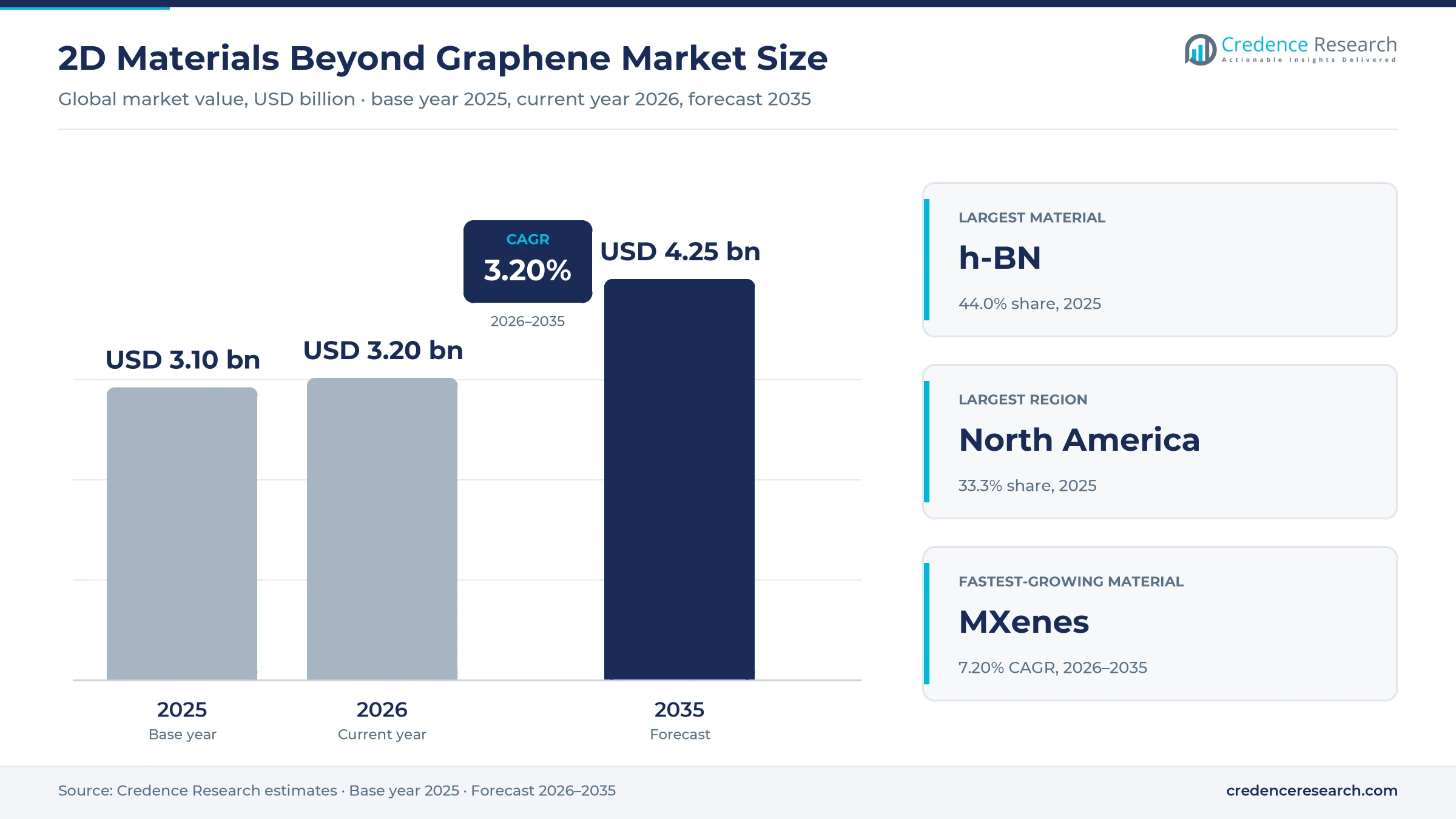
Sales of 2D materials other than graphene reached USD 3.10 billion in 2025, and Credence Research expects USD 4.25 billion by 2035, a modest 3.20% CAGR over 2026–2035, with USD 3.20 billion estimated for 2026. Most of today's value comes from hexagonal boron nitride (h-BN) and molybdenum disulfide (MoS2) powders used in coatings, composites and thermal management, while electronics-grade films remain a small research-driven niche.
The gap between the two halves of the market explains the slow headline growth. Industrial powders grow with manufacturing output, while wafer-scale films for chips grow fast but from a tiny base.
Which materials does the market include?
The market covers layered materials, other than graphene, supplied as monolayer or few-layer films, exfoliated nanosheets, dispersions and engineered powders. The scope includes:
- Transition metal dichalcogenides such as MoS2, WS2 and WSe2, hexagonal boron nitride, MXenes such as Ti3C2Tx, black phosphorus and other 2D materials.
- Material made by chemical vapor deposition (CVD), exfoliation, molecular beam epitaxy or physical vapor deposition, and solution synthesis.
- Films and coatings, powders and flakes, dispersions and inks, and wafers or substrates.
The scope excludes graphene, graphene oxide and graphene nanoplatelets, which belong to the graphene market, as well as bulk molybdenum and boron chemicals not processed into 2D form. Values are material sales in USD billion at current prices, allocated to the region of the buyer. The wider family is covered in the 2D materials market.
How was the estimate built?
All figures are Credence Research estimates, built from end-use consumption of h-BN and MoS2 grades, supplier price lists, pilot-line volumes and research funding, and checked against supplier disclosures.
What do public indicators show?
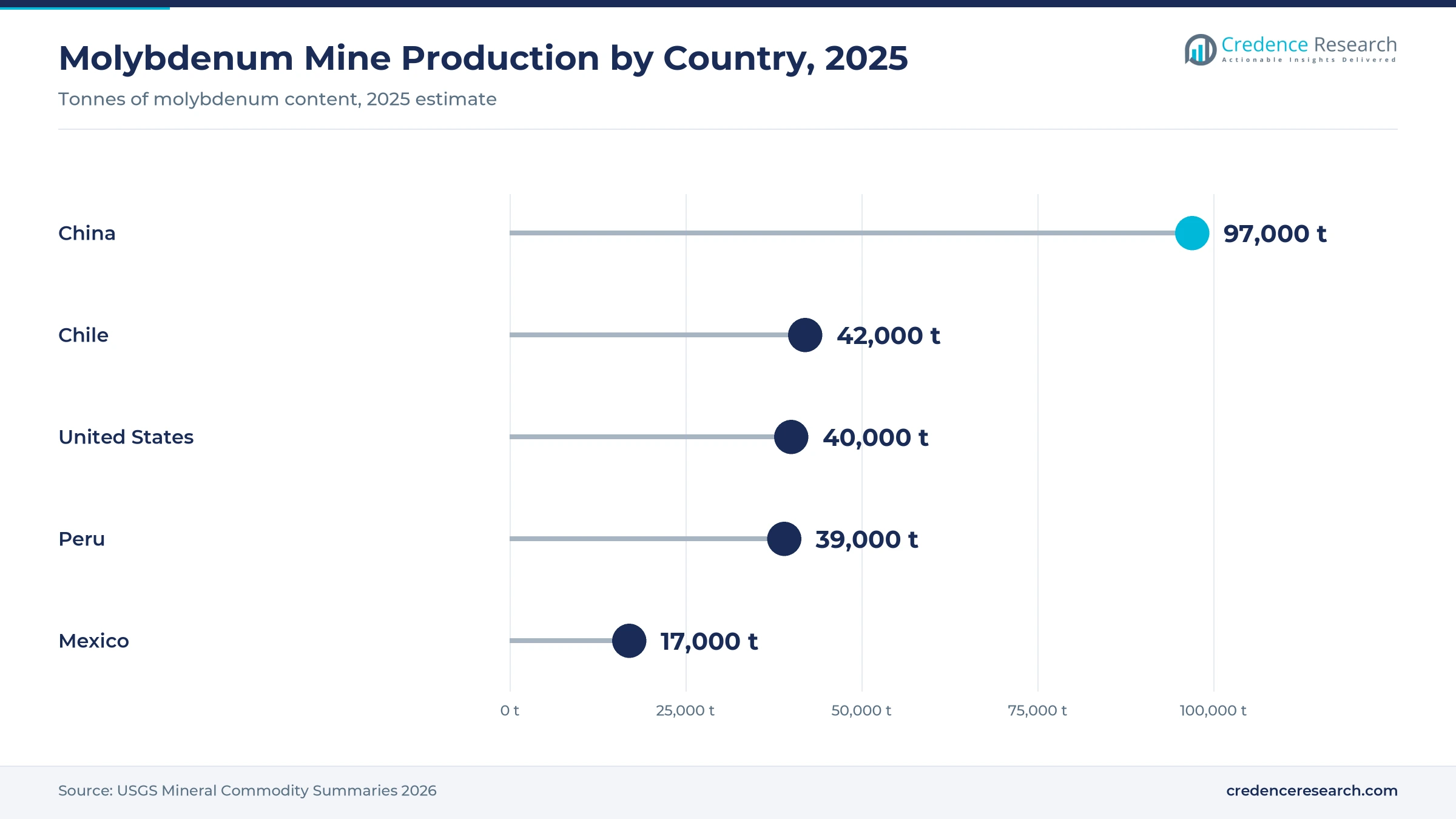
Precursor supply is ample. World molybdenum mine production reached an estimated 260,000 tonnes in 2025, up from 256,000 tonnes in 2024, according to the USGS Mineral Commodity Summaries 2026. Boron, the h-BN feedstock, was added to the US critical minerals list in November 2025.
Report Attributes
| Attribute | Details |
|---|---|
| Historical Period | 2018–2024 |
| Base Year | 2025 |
| Forecast Period | 2026–2035 |
| Market Size 2025 | USD 3.10 billion |
| Market Size 2026 (estimate) | USD 3.20 billion |
| Market Size 2035 (forecast) | USD 4.25 billion |
| CAGR (2026–2035) | 3.20% |
| Segments Covered | By Material, By End Use, By Application, By Production Method, By Product Form, By Customer |
| Regions Covered | North America, Europe, Asia Pacific, Latin America, Middle East & Africa |
| Companies Covered | 2D Semiconductors Inc., Graphenea S.A., NanoXplore Inc., Sixth Element Materials Technology Co., Ltd., Versarien plc, 2D Layer Materials Pte. Ltd., XG Sciences, Inc., ACS Material, LLC, Thomas Swan & Co. Ltd. |
2D Materials Beyond Graphene Market Insights
- The 2D materials beyond graphene market was worth USD 3.10 billion in 2025 and is forecast to reach USD 4.25 billion by 2035, a 3.20% CAGR over 2026–2035.
- Credence Research estimates the market at USD 3.20 billion in 2026, the current year.
- Hexagonal boron nitride leads with a 44.0% share; MXenes grow fastest at 7.20% a year.
- Coatings and composites hold 56.0% of 2025 value; transistors and logic grow fastest at 8.57%.
- North America is the largest region at 33.3%; Asia Pacific grows fastest at 3.82%.
- Chip scaling is the strongest driver, adding about 1.0 percentage point to the forecast CAGR.
Boron Nitride Powders for Coatings and Composites Hold Most of the Value
Which material leads?
Hexagonal boron nitride leads with a 44.0% share in 2025, thanks to its use in thermal fillers, lubricant coatings and cosmetics-grade powders. Transition metal dichalcogenides follow, while black phosphorus and other materials remain small. MXenes grow fastest at 7.20% a year.
Which end use leads?
Electronics and electrical uses lead with a 38.0% share. Automotive, aerospace and defense, and healthcare follow. Energy and power grows fastest at 4.11% a year.
Which application leads?
Coatings and composites lead with a 56.0% share. Batteries and supercapacitors, sensors and photodetectors, and membranes follow. Transistors and logic grow fastest at 8.57% a year from a small base.
Which production method and form lead?
Exfoliation leads production methods with a 52.0% share, since most powders and nanosheets are exfoliated from bulk crystals. Powders and flakes lead product forms with a 58.0% share.
Which customer group leads?
Materials suppliers that blend 2D materials into coatings, lubricants and composites lead with a 34.0% share. Energy companies grow fastest at 3.94% a year.
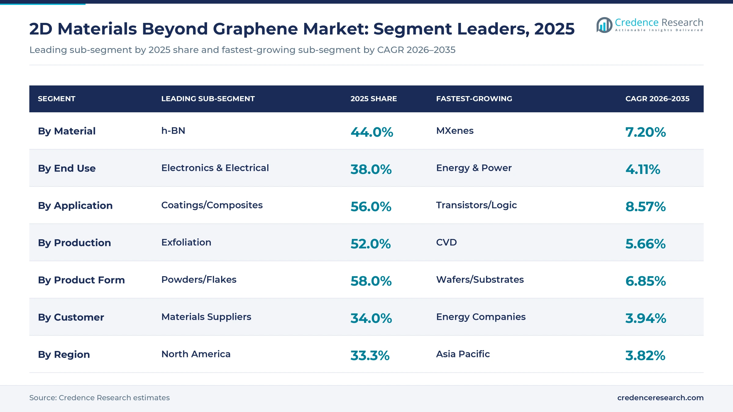
| Segment Group | Leading Sub-segment | 2025 Share | Fastest-growing Sub-segment | CAGR 2026–2035 |
|---|---|---|---|---|
| By Material | h-BN | 44.0% | MXenes | 7.20% |
| By End Use | Electronics & Electrical | 38.0% | Energy & Power | 4.11% |
| By Application | Coatings/Composites | 56.0% | Transistors/Logic | 8.57% |
| By Production Method | Exfoliation | 52.0% | CVD | 5.66% |
| By Product Form | Powders/Flakes | 58.0% | Wafers/Substrates | 6.85% |
| By Customer | Materials Suppliers | 34.0% | Energy Companies | 3.94% |
Request a Free Sample
Fill in your details and we'll send you a free sample report.
- Sample data tables & charts
- Research methodology
Smaller Transistors, Public Research Funding and Battery Materials Support Demand
Why does chip scaling matter? (~+1.0% impact on forecast CAGR)
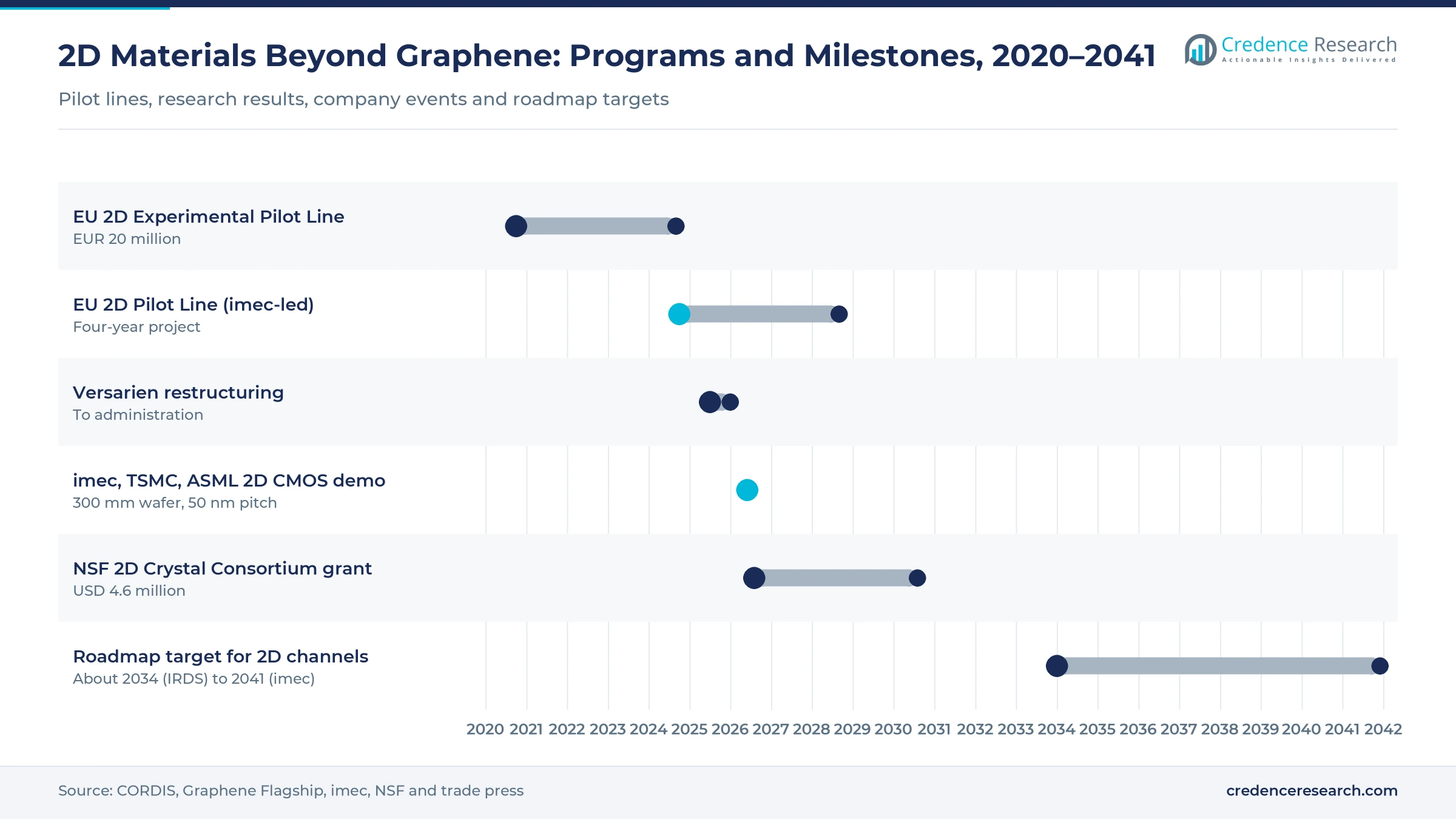
Demand for smaller, more energy-efficient electronics is the strongest driver, adding an estimated 1.0 percentage point to the forecast CAGR. Silicon channels lose control of current when they become only a few atoms thick, while 2D semiconductors stay stable at that thickness. In June 2026, imec, TSMC and ASML showed complementary transistors with 2D channels on one 300 mm wafer at a 50 nm contacted poly pitch, with 94% of devices working, according to an imec announcement. Transistors and logic are the fastest-growing application at 8.57% a year. The limit is time: industry roadmaps place 2D channels in production in the mid-2030s or later, so most chip demand falls at the end of the forecast.
How does research funding help? (~+0.8% impact on forecast CAGR)
Government and private funding for nanomaterials research and commercialization adds about 0.8 percentage points to the forecast CAGR. The EU's 2D Experimental Pilot Line received EUR 20 million from 2020 to 2024, as recorded by CORDIS, and its successor pilot line started in October 2024 for four years. In the United States, NSF awarded Penn State USD 4.6 million in August 2026 to make its 2D Crystal Consortium self-sustaining. Research and academic buyers account for a meaningful share of electronics-grade demand. The condition is follow-on money: pilot lines need industrial customers to survive once grants end.
Why are batteries and supercapacitors important? (~+0.6% impact on forecast CAGR)
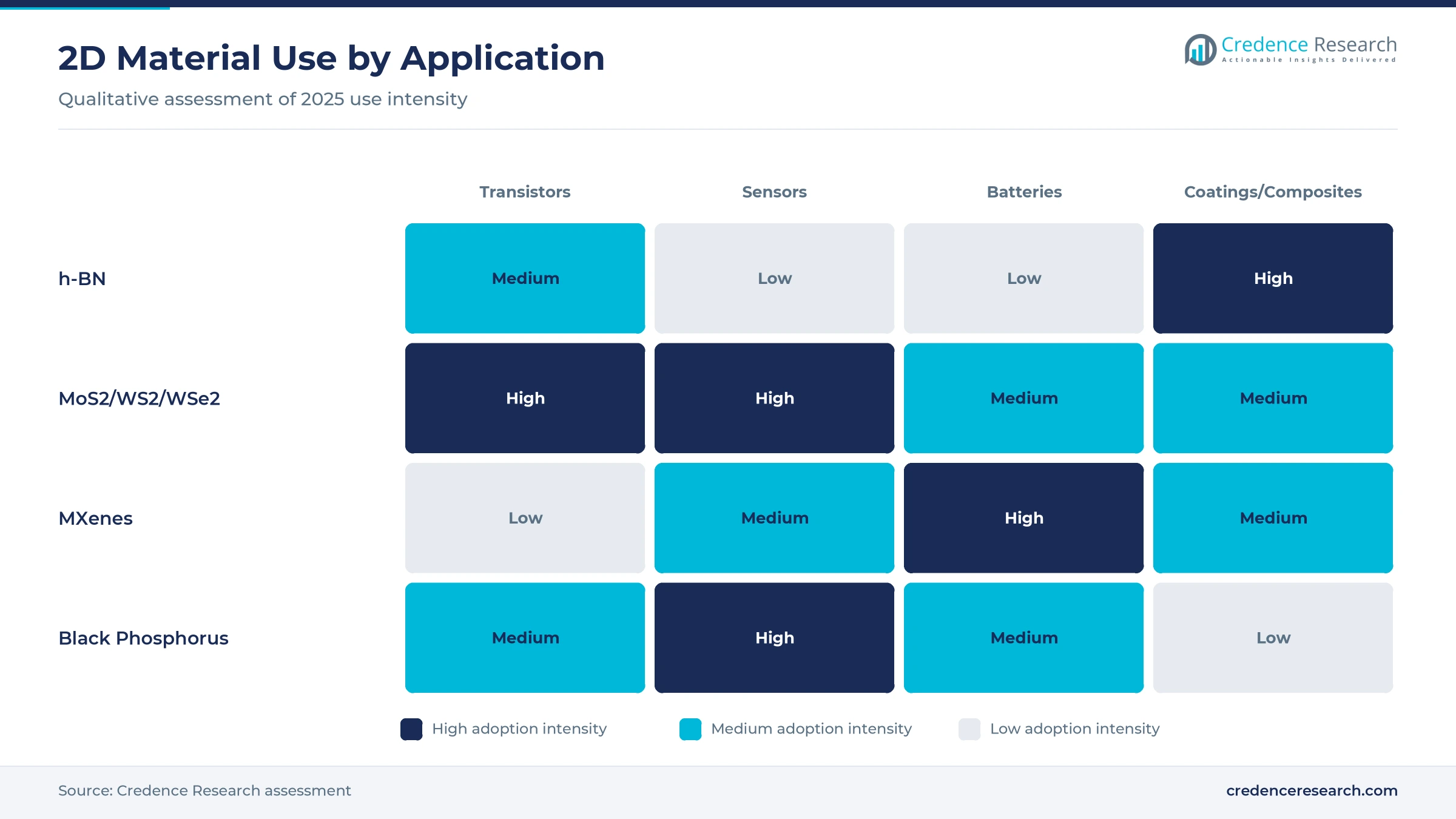
Use of 2D materials in batteries, supercapacitors and other energy systems adds about 0.6 percentage points to the forecast CAGR. MXenes conduct electricity well and store charge on their large surfaces, which makes them candidates for fast-charging electrodes and electromagnetic shielding. MXenes are the fastest-growing material at 7.20% a year, and energy and power is the fastest-growing end use at 4.11%. Scale-up remains the hurdle, because most MXene production still uses small batch processes and MXenes oxidize when stored in water. Molybdenum disulfide and tungsten disulfide are also being tested as anode and catalyst materials, but these uses have not yet reached commercial volumes.
Wafer-Scale Growth, Lower Temperatures and Supplier Consolidation
Trend 1: Is growth moving to full wafers?
Yes. European pilot-line partners showed TMD monolayers grown on 300 mm wafers at SEMICON Europa in November 2025. Wafers and substrates are the fastest-growing product form at 6.85% a year, and CVD is the fastest-growing production method at 5.66%.
Trend 2: Can 2D films be grown at low temperatures?
MIT spin-out CDimension grows single-layer MoS2 at about 200 °C on 300 mm silicon, compared with more than 1,000 °C for typical processes, as reported by IEEE Spectrum. Low-temperature growth could let chipmakers add 2D layers on top of finished circuits. CDimension named three US universities as its first wafer customers in August 2025.
Trend 3: Is the supplier base consolidating?
Yes. Several small nanomaterial firms closed or were sold. Versarien plc entered administration in January 2026, and graphene producer XG Sciences ceased operations in 2022, with NanoXplore buying its assets. Buyers increasingly favor suppliers with stable finances and repeatable quality.
Trend 4: Are MXenes moving toward production?
Companies are licensing faster MXene synthesis methods from universities, aiming at shielding and energy storage. These projects remain at an early, pre-commercial stage.
Transfer, Contacts and Thin Commercial Demand Hold Back Scale-Up
Why is device integration hard?
Most 2D transistors today use films grown on one substrate and transferred to another. Transfer leaves residues and defects, and low-resistance metal contacts to 2D layers remain an open problem. Until these are solved, chipmakers will not commit to volume orders.
Why is demand thin?
Outside industrial powders, demand comes mainly from research groups buying small quantities of films and crystals. Supplier price lists show four-inch MoS2 wafers at around USD 2,000 each, which suits research budgets but not production. Thin demand keeps suppliers small and vulnerable.
Are suppliers financially fragile?
Yes. Versarien's administration and the closure of other small producers show how hard it is to fund scale-up before large customers arrive. Buyers face supply risk when a qualified source exits.
Do standards exist?
Few. Layer count, defect density and purity are measured differently by each supplier, which slows qualification by industrial buyers.
Where are the opportunities?
Thermal management in power electronics and data centers needs better electrically insulating fillers. Suppliers of high-purity h-BN nanosheets that disperse well in polymers can win this demand. The execution risk is cost against conventional ceramic fillers, which are cheaper. See also the hexagonal boron nitride market.
North America and Asia Pacific Lead, With Europe Close Behind
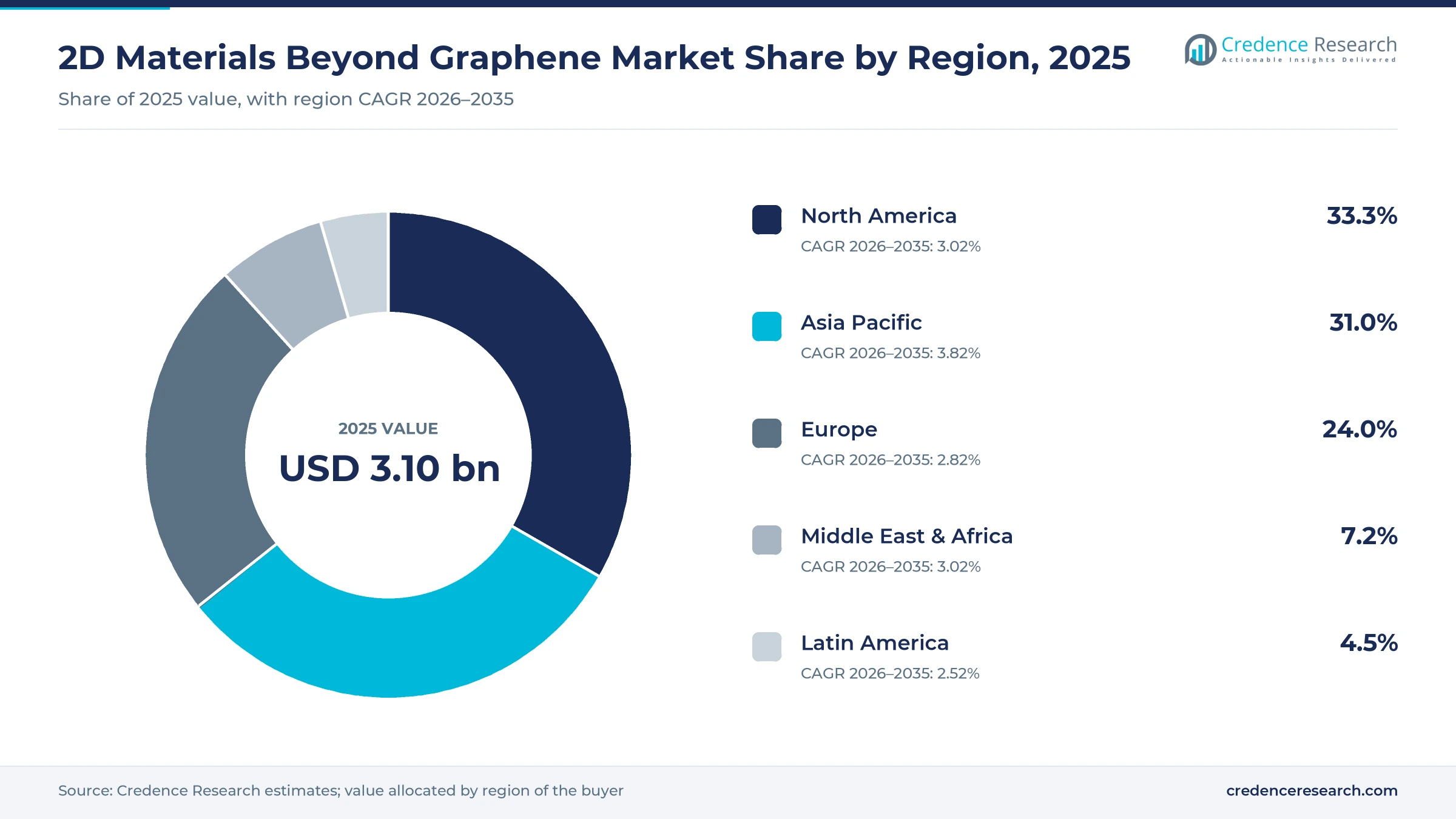
Value is allocated to the region of the buyer.
| Region | Share 2025 | CAGR 2026–2035 |
|---|---|---|
| North America | 33.3% | 3.02% |
| Asia Pacific | 31.0% | 3.82% |
| Europe | 24.0% | 2.82% |
| Middle East & Africa | 7.2% | 3.02% |
| Latin America | 4.5% | 2.52% |
Why does North America lead?
North America holds a 33.3% share in 2025 and grows at 3.02% a year. Research universities, national laboratories and defense programs buy electronics-grade films, and several merchant suppliers, including 2D Semiconductors, ACS Material and CDimension, are based in the United States.
Why is Asia Pacific growing fastest?
Asia Pacific holds 31.0% and is the fastest-growing region at 3.82% a year. China, Japan and South Korea consume large volumes of h-BN and MoS2 powders in electronics and batteries, and Taiwanese foundries co-develop 2D transistors with European research centers.
What shapes Europe?
Europe holds 24.0% and grows at 2.82% a year. EU-funded pilot lines coordinated by imec, and tool makers in Germany and Austria, anchor the region's role in wafer-scale integration.
What about Latin America and the Middle East & Africa?
Latin America holds 4.5% and grows at 2.52%. Chile, Peru and Mexico supply molybdenum but consume little 2D material. The Middle East & Africa region holds 7.2% and grows at 3.02%, with Turkey a major producer of borates for h-BN.
Research Milestones, Funding and Supplier Changes, 2025–2026
| Development | Status and why it matters |
|---|---|
| In August 2026, NSF awarded Penn State USD 4.6 million over four years to make its 2D Crystal Consortium self-sustaining. | Awarded. Supports US research supply of 2D crystals. |
| In June 2026, imec, TSMC and ASML announced complementary 2D-channel transistors on a 300 mm wafer at a 50 nm contacted poly pitch, with 94% of devices working. | Research result. Moves 2D logic closer to industrial processes. |
| In January 2026, Versarien plc entered administration after its sale process found no going-concern buyer. | In administration. Removes a UK nanomaterials supplier. |
| In December 2025, imec presented WSe2 pFETs made with TSMC-supplied layers and 300 mm-compatible contact modules developed with Intel at IEDM. | Research result. Addresses the contact problem. |
| In November 2025, the European 2D Pilot Line showed TMD monolayers grown on 300 mm wafers at SEMICON Europa. | Pilot. Demonstrates wafer-scale growth. |
| In October 2025, the 2D Pilot Line launched a support program offering up to 50% off multi-project wafer fees. | Launched. Lowers the cost of first device trials. |
| In August 2025, CDimension announced its first university customers for wafer-scale MoS2 and a partnership with PSMC on test circuits. | Early commercial. Shows merchant supply of 2D wafers. |
| In July 2025, IEEE Spectrum reported CDimension's MoS2 growth at about 200 °C on 300 mm wafers. | Reported. Points to back-end integration. |
Need a Custom Version of This Report?
Tailor the scope, geography, or segments to your exact requirements.
- Custom geography or segment scope
- Direct access to our analyst team
Small Specialist Suppliers Serve a Research-Led Market
The supplier base is fragmented and mostly small, and several companies often grouped with this market sell mainly graphene. No share ranking is given because suppliers do not disclose comparable sales.
Who supplies electronics-grade 2D materials?
2D Semiconductors Inc. sells bulk crystals, CVD and MBE films, inks and powders of MoS2, WS2, WSe2, h-BN and other layered materials. 2D Layer Materials supplies wafer-scale TMD films in sizes up to eight inches. ACS Material, LLC sells catalogue quantities of MoS2, MoSe2, h-BN and MXene alongside graphene.
Which listed companies are graphene-focused?
Graphenea S.A., NanoXplore Inc. and Sixth Element Materials Technology Co., Ltd. focus on graphene products, although Graphenea takes part in European 2D pilot-line wafer runs. Thomas Swan & Co. Ltd. is known for carbon nanomaterials. Versarien plc entered administration in January 2026, and XG Sciences, Inc. ceased operations in 2022 before NanoXplore acquired its assets. Their role in beyond-graphene materials is limited.
Who else shapes the market?
Research centers and chipmakers, including imec, TSMC and Intel, drive device development and buy small volumes. Large chemical companies supply industrial h-BN and MoS2 powders for coatings and lubricants. Tool makers such as Aixtron, EV Group and SUSS MicroTec provide growth and transfer equipment, and their pilot-line work with imec helps set the process recipes that future material suppliers will need to meet.
How do suppliers compete?
Suppliers compete on layer control, purity, wafer size and price. Those that can supply consistent wafer-scale films to chipmakers, or high-volume nanosheets to industrial buyers, are best placed. Device research is covered in the 2D material transistor market.
Frequently Asked Questions
How big is the 2D materials beyond graphene market?
Which materials are included?
Why is growth modest?
What drives the market?
Which region leads?
When will 2D transistors reach production?
Table of Content
Chapter 1 Market Segmentation
- 1.1 Segmentation Framework
- 1.1.1 Product and Service Classification
- 1.1.2 Application and End-Use Classification
- 1.1.3 Technology and Solution Classification
- 1.1.4 Customer and Distribution Channel Classification
- 1.1.5 Geographic Segmentation
- 1.1.6 Market Segment Definitions and Boundaries
- 1.2 By Material
- 1.2.1 Transition Metal Dichalcogenides (MoS2, WS2, WSe2)
- 1.2.2 h-BN
- 1.2.3 MXenes
- 1.2.4 Black Phosphorus
- 1.2.5 Other 2D Materials
- 1.3 By End Use
- 1.3.1 Electronics & Electrical
- 1.3.2 Energy & Power
- 1.3.3 Aerospace & Defense
- 1.3.4 Automotive
- 1.3.5 Healthcare
- 1.4 By Application
- 1.4.1 Transistors/Logic
- 1.4.2 Sensors/Photodetectors
- 1.4.3 Batteries/Supercapacitors
- 1.4.4 Coatings/Composites
- 1.4.5 Membranes
- 1.5 By Production Method
- 1.5.1 CVD
- 1.5.2 Exfoliation
- 1.5.3 MBE/PVD
- 1.5.4 Solution/Chemical Synthesis
- 1.6 By Product Form
- 1.6.1 Films/Coatings
- 1.6.2 Powders/Flakes
- 1.6.3 Dispersions/Inks
- 1.6.4 Wafers/Substrates
- 1.7 By Customer
- 1.7.1 Semiconductor/Electronics OEMs
- 1.7.2 Energy Companies
- 1.7.3 Materials Suppliers
- 1.7.4 R&D/Academia
Chapter 2 Introduction
- 2.1 Report Objectives and Scope
- 2.2 Product Definition and Industry Terminology
- 2.3 Market Inclusions and Exclusions
- 2.4 Research Process
- 2.4.1 Primary Research and Expert Interviews
- 2.4.2 Secondary Research and Source Review
- 2.4.3 Top-Down and Bottom-Up Estimation
- 2.4.4 Data Triangulation and Verification
- 2.5 Market Size Measurement Basis
- 2.5.1 2025: USD 3.10 billion → 2035: USD 4.25 billion
- 2.6 Historical and Forecast Reference Periods
- 2.6.1 Historical Period: 2018-2025
- 2.6.2 Base Year: 2025
- 2.6.3 Forecast Period: 2025-2035
- 2.7 Research Assumptions and Limitations
Chapter 3 Executive Summary
- 3.1 Market Snapshot and Key Findings
- 3.2 Base-Year Market Size, 2025
- 3.3 Forecast Market Size, 2035
- 3.4 Revenue and Volume Growth Outlook
- 3.5 Key Demand and Supply Indicators
- 3.6 Leading Market Segments
- 3.7 Fastest-Growing Market Opportunities
- 3.8 Regional Performance Highlights
- 3.9 Technology and Industry Transformation
- 3.10 Competitive Landscape Summary
- 3.11 Analyst View and Strategic Implications
Chapter 4 Global 2D Materials Beyond Graphene Market Trends and Developments
- 4.1 Historical Industry Development, 2018-2025
- 4.2 Recent Market Trends and Developments
- 4.3 Demand and Customer Behavior Trends
- 4.4 Technology and Product Innovation
- 4.5 Artificial Intelligence, Automation and Digitalization
- 4.6 Local Manufacturing and Supply Chain Realignment
- 4.7 Industry Partnerships, Mergers and Acquisitions
- 4.8 Sustainability and Circular Economy Developments
- 4.9 Government and Private Sector Investment Trends
- 4.10 Emerging Business Models and Commercialization
- 4.11 Industry Developments and Announcements
Chapter 5 Global 2D Materials Beyond Graphene Market Production, Supply and Demand Analysis
- 5.1 Demand Trend and Consumption Analysis, 2018-2025
- 5.2 Demand Forecast, 2025-2035
- 5.3 Production and Output Trend, 2018-2025
- 5.4 Production and Output Forecast, 2025-2035
- 5.5 Installed Capacity and Capacity Utilization
- 5.6 Company-Wise Production Plants and Statistics
- 5.6.1 Installed Production Capacity
- 5.6.2 Actual Production
- 5.6.3 Planned Capacity and Expansion Targets
- 5.7 Supply Chain Structure and Procurement Trends
- 5.8 Supply-Demand Gap and Bottlenecks
- 5.9 Import Dependence and Sourcing Structure
- 5.10 Contract Manufacturing and Outsourcing
- 5.11 Regional Supply and Demand Concentration
Chapter 6 Global 2D Materials Beyond Graphene Market Pricing Analysis
- 6.1 Pricing Structure and Measurement
- 6.2 Historical Pricing Trends, 2018-2025
- 6.3 Pricing Outlook, 2025-2035
- 6.4 Average Selling Price and Unit Economics
- 6.5 Pricing by Product and Market Segment
- 6.6 Geographic Pricing Differences
- 6.7 Key Input, Energy, Labor and Logistics Costs
- 6.8 Contract Pricing and Purchasing Models
- 6.9 Pricing Sensitivity and Competitive Positioning
- 6.10 Price, Margin and Profitability Implications
Chapter 7 Global 2D Materials Beyond Graphene Market Dynamics
- 7.1 Market Growth Drivers
- 7.1.1 Demand-Side Drivers
- 7.1.2 Technology and Innovation Drivers
- 7.1.3 Infrastructure and Investment Drivers
- 7.1.4 Regulatory and Policy Drivers
- 7.2 Market Restraints
- 7.2.1 Cost and Affordability Constraints
- 7.2.2 Technology and Adoption Barriers
- 7.2.3 Supply Chain and Operational Constraints
- 7.3 Market Challenges
- 7.3.1 Competitive Pressure and Margin Erosion
- 7.3.2 Skills, Infrastructure and Implementation Gaps
- 7.4 Emerging Market Opportunities
- 7.5 Market Dynamics Impact and Time-Horizon Assessment
Chapter 8 Global 2D Materials Beyond Graphene Value Chain Analysis
- 8.1 Industry Value Chain Overview
- 8.2 Upstream Suppliers and Critical Inputs
- 8.3 Technology and Component Providers
- 8.4 Manufacturing or Service Delivery
- 8.5 Distribution, Channel Partners and Integrators
- 8.6 Downstream Applications and End Users
- 8.7 Value Addition and Profit Pools
- 8.8 Vertical Integration and Outsourcing
- 8.9 Supplier Concentration and Risk
- 8.10 Supply Chain Localization and Resilience
Chapter 9 Global 2D Materials Beyond Graphene Market Regulations and Policies
- 9.1 Relevant Laws, Standards and Compliance Frameworks
- 9.2 Product, Service, Safety and Quality Requirements
- 9.3 Government Policies, Incentives and Subsidies
- 9.4 Imports, Exports and Trade Barriers
- 9.5 Public Procurement and Local Content Requirements
- 9.6 Environmental and Sustainability Compliance
- 9.7 Upcoming Policy Changes and Market Implications
Chapter 10 Global 2D Materials Beyond Graphene Market Hotspots and Opportunities
- 10.1 Market Opportunity Mapping and Growth Hotspots
- 10.2 High-Growth Applications and Customer Groups
- 10.3 Underserved Markets and White-Space Opportunities
- 10.4 Emerging Technology and Product Opportunities
- 10.5 New Capacity and Investment Hotspots
- 10.6 Market Entry and Expansion Opportunities
- 10.7 Distribution and Partnership Opportunities
- 10.8 Near-Term and Long-Term Commercial Potential
- 10.9 Opportunity Attractiveness and Execution Risks
Chapter 11 Global 2D Materials Beyond Graphene Market Outlook, 2025-2035
- 11.1 Market Size and Analysis
- 11.1.1 Revenue (Market Measurement: 2025: USD 3.10 billion → 2035: USD 4.25 billion)
- 11.1.2 Market Volume and Quantity Sold
- 11.1.3 Historical Market Size, 2018-2025
- 11.1.4 Base-Year Market Size, 2025
- 11.2 Market Forecast, 2025-2035
- 11.2.1 Revenue Forecast to 2035
- 11.2.2 Volume Forecast to 2035
- 11.2.3 CAGR and Year-on-Year Growth
- 11.2.4 Incremental Revenue Opportunity
- 11.3 Forecast Assumptions and Scenario Analysis
- 11.3.1 Base-Case Forecast
- 11.3.2 Optimistic and Conservative Scenarios
- 11.3.3 Technology, Pricing and Policy Sensitivities
- 11.4 Market Attractiveness and Growth Outlook
Chapter 12 Global 2D Materials Beyond Graphene Market Segmentation and Outlook
- 12.1 Segmentation Summary and Market Shares, 2025
- 12.2 Largest and Fastest-Growing Segments
- 12.3 By Material - Market Size and Forecast, 2025-2035
- 12.3.1 Segment Definition and Scope
- 12.3.2 Historical Market Size, 2018-2025
- 12.3.3 Revenue Forecast, 2025-2035
- 12.3.4 Volume Forecast, 2025-2035
- 12.3.5 Base-Year Market Share, 2025
- 12.3.6 Segment CAGR and Growth Drivers
- 12.3.7 Subsegment Market Size and Forecast
- 12.3.7.1 Transition Metal Dichalcogenides (MoS2, WS2, WSe2)
- 12.3.7.2 h-BN
- 12.3.7.3 MXenes
- 12.3.7.4 Black Phosphorus
- 12.3.7.5 Other 2D Materials
- 12.3.8 Subsegment Pricing and Adoption Trends
- 12.3.9 Leading Suppliers and Competition
- 12.3.10 Regional Demand and Opportunities
- 12.4 By End Use - Market Size and Forecast, 2025-2035
- 12.4.1 Segment Definition and Scope
- 12.4.2 Historical Market Size, 2018-2025
- 12.4.3 Revenue Forecast, 2025-2035
- 12.4.4 Volume Forecast, 2025-2035
- 12.4.5 Base-Year Market Share, 2025
- 12.4.6 Segment CAGR and Growth Drivers
- 12.4.7 Subsegment Market Size and Forecast
- 12.4.7.1 Electronics & Electrical
- 12.4.7.2 Energy & Power
- 12.4.7.3 Aerospace & Defense
- 12.4.7.4 Automotive
- 12.4.7.5 Healthcare
- 12.4.8 Subsegment Pricing and Adoption Trends
- 12.4.9 Leading Suppliers and Competition
- 12.4.10 Regional Demand and Opportunities
- 12.5 By Application - Market Size and Forecast, 2025-2035
- 12.5.1 Segment Definition and Scope
- 12.5.2 Historical Market Size, 2018-2025
- 12.5.3 Revenue Forecast, 2025-2035
- 12.5.4 Volume Forecast, 2025-2035
- 12.5.5 Base-Year Market Share, 2025
- 12.5.6 Segment CAGR and Growth Drivers
- 12.5.7 Subsegment Market Size and Forecast
- 12.5.7.1 Transistors/Logic
- 12.5.7.2 Sensors/Photodetectors
- 12.5.7.3 Batteries/Supercapacitors
- 12.5.7.4 Coatings/Composites
- 12.5.7.5 Membranes
- 12.5.8 Subsegment Pricing and Adoption Trends
- 12.5.9 Leading Suppliers and Competition
- 12.5.10 Regional Demand and Opportunities
- 12.6 By Production Method - Market Size and Forecast, 2025-2035
- 12.6.1 Segment Definition and Scope
- 12.6.2 Historical Market Size, 2018-2025
- 12.6.3 Revenue Forecast, 2025-2035
- 12.6.4 Volume Forecast, 2025-2035
- 12.6.5 Base-Year Market Share, 2025
- 12.6.6 Segment CAGR and Growth Drivers
- 12.6.7 Subsegment Market Size and Forecast
- 12.6.7.1 CVD
- 12.6.7.2 Exfoliation
- 12.6.7.3 MBE/PVD
- 12.6.7.4 Solution/Chemical Synthesis
- 12.6.8 Subsegment Pricing and Adoption Trends
- 12.6.9 Leading Suppliers and Competition
- 12.6.10 Regional Demand and Opportunities
- 12.7 By Product Form - Market Size and Forecast, 2025-2035
- 12.7.1 Segment Definition and Scope
- 12.7.2 Historical Market Size, 2018-2025
- 12.7.3 Revenue Forecast, 2025-2035
- 12.7.4 Volume Forecast, 2025-2035
- 12.7.5 Base-Year Market Share, 2025
- 12.7.6 Segment CAGR and Growth Drivers
- 12.7.7 Subsegment Market Size and Forecast
- 12.7.7.1 Films/Coatings
- 12.7.7.2 Powders/Flakes
- 12.7.7.3 Dispersions/Inks
- 12.7.7.4 Wafers/Substrates
- 12.7.8 Subsegment Pricing and Adoption Trends
- 12.7.9 Leading Suppliers and Competition
- 12.7.10 Regional Demand and Opportunities
- 12.8 By Customer - Market Size and Forecast, 2025-2035
- 12.8.1 Segment Definition and Scope
- 12.8.2 Historical Market Size, 2018-2025
- 12.8.3 Revenue Forecast, 2025-2035
- 12.8.4 Volume Forecast, 2025-2035
- 12.8.5 Base-Year Market Share, 2025
- 12.8.6 Segment CAGR and Growth Drivers
- 12.8.7 Subsegment Market Size and Forecast
- 12.8.7.1 Semiconductor/Electronics OEMs
- 12.8.7.2 Energy Companies
- 12.8.7.3 Materials Suppliers
- 12.8.7.4 R&D/Academia
- 12.8.8 Subsegment Pricing and Adoption Trends
- 12.8.9 Leading Suppliers and Competition
- 12.8.10 Regional Demand and Opportunities
- 12.9 Segment Growth Comparison
- 12.10 Segment Attractiveness and Priority Matrix
Chapter 13 Global 2D Materials Beyond Graphene End-Use and Application Market Outlook
- 13.1 End-Use Industry and Customer Demand Structure
- 13.2 Leading Applications and Customer Groups
- 13.3 End-Use Market Size, Share and Forecast
- 13.4 Major End-Use Industry Deep Dives
- 13.4.1 Customer Requirements and Use Cases
- 13.4.2 Demand and Replacement Cycles
- 13.4.3 Technical and Regulatory Considerations
- 13.4.4 Purchasing and Procurement Models
- 13.4.5 Leading Vendors and Distribution Channels
- 13.4.6 Forecast and Commercial Opportunities
- 13.5 Emerging Applications and Cross-Segment Demand
- 13.6 End-Use Industry Investment Priorities
Chapter 14 Global 2D Materials Beyond Graphene Geographic Market Outlook, 2025-2035
- 14.1 Regional Market Size and Share, 2025
- 14.2 Regional Market Forecast, 2025-2035
- 14.3 Regional Pricing, Production and Demand Differences
- 14.4 North America
- 14.4.1 United States
- 14.4.2 Canada
- 14.4.3 Mexico
- 14.5 Europe
- 14.5.1 Germany
- 14.5.2 France
- 14.5.3 Italy
- 14.5.4 United Kingdom
- 14.5.5 Spain
- 14.5.6 Poland
- 14.5.7 Russia
- 14.5.8 Netherlands
- 14.5.9 Belgium
- 14.5.10 Sweden
- 14.5.11 Denmark
- 14.5.12 Norway
- 14.5.13 Rest of Europe
- 14.6 Asia Pacific
- 14.6.1 China
- 14.6.2 India
- 14.6.3 Japan
- 14.6.4 South Korea
- 14.6.5 Thailand
- 14.6.6 Indonesia
- 14.6.7 Vietnam
- 14.6.8 Malaysia
- 14.6.9 Australia
- 14.6.10 Rest of Asia Pacific
- 14.7 Latin America
- 14.7.1 Brazil
- 14.7.2 Argentina
- 14.7.3 Colombia
- 14.7.4 Chile
- 14.7.5 Rest of Latin America
- 14.8 Middle East
- 14.8.1 Saudi Arabia
- 14.8.2 United Arab Emirates
- 14.8.3 Turkey
- 14.8.4 Israel
- 14.8.5 Iran
- 14.8.6 Rest of the Middle East
- 14.9 Africa
- 14.9.1 South Africa
- 14.9.2 Egypt
- 14.9.3 Nigeria
- 14.9.4 Morocco
- 14.9.5 Rest of Africa
- 14.10 Regional Investment, Policy and Supply Chain Differences
- 14.11 Regional Competitive Landscape
- 14.12 Geographic Growth Hotspots
Chapter 15 Global 2D Materials Beyond Graphene Technology, Innovation and Sustainability Outlook
- 15.1 Technology Landscape and Maturity
- 15.2 Product, Process and Service Innovation
- 15.3 AI, Automation and Digital Tools in the Industry
- 15.4 Technology Adoption and Performance Benchmarking
- 15.5 Innovation Pipeline and R&D Investment
- 15.6 Patent and Intellectual Property Trends
- 15.7 Energy Efficiency and Resource Management
- 15.8 Sustainability, Recycling and Circularity
- 15.9 Technology Roadmap, 2025-2035
- 15.10 Risks of Obsolescence and Technology Substitution
Chapter 16 Global 2D Materials Beyond Graphene Market Key Strategic Imperatives
- 16.1 Growth and Market Entry Priorities
- 16.2 High-Return Products and Segments
- 16.3 Pricing, Profitability and Cost Optimization
- 16.4 Technology Investment and Product Differentiation
- 16.5 Supply Chain Localization and Resilience
- 16.6 Distribution and Customer Acquisition
- 16.7 Partnership, Acquisition and Capacity Strategy
- 16.8 Regional Expansion Priorities
- 16.9 Short-, Medium- and Long-Term Actions
Chapter 17 Competition Outlook
- 17.1 Industry Competition Characteristics
- 17.2 Market Structure and Concentration
- 17.3 Market Share and Competitive Positioning, 2025
- 17.4 Company-Wise Revenue and Product Benchmarking
- 17.5 Production and Service Capacity Benchmarking
- 17.6 Technology, Pricing and Differentiation
- 17.7 Regional Footprint and Distribution Strength
- 17.8 Mergers, Acquisitions and Strategic Alliances
- 17.9 New Entrants and Competitive Threats
- 17.10 Porter's Five Forces and Industry Attractiveness
- 17.11 Competitive Outlook, 2025-2035
Chapter 18 Company Profiles
- 18.1 Company Coverage and Selection Criteria
- 18.2 2D Semiconductors Inc.
- 18.2.1 Business Description
- 18.2.2 Company Ownership and Geographic Presence
- 18.2.3 Product and Service Portfolio
- 18.2.4 Manufacturing and Operating Footprint
- 18.2.5 Production Capacity and Expansion Plans
- 18.2.6 Financial Performance and Investment
- 18.2.7 Market Share and Competitive Position
- 18.2.8 Technology and Innovation Capabilities
- 18.2.9 Strategic Alliances or Partnerships
- 18.2.10 Recent Developments
- 18.2.11 Growth Strategy and Outlook
- 18.3 Graphenea S.A.
- 18.4 NanoXplore Inc.
- 18.5 Sixth Element Materials Technology Co., Ltd.
- 18.6 Versarien plc
- 18.7 2D Layer Materials Pte. Ltd.
- 18.8 XG Sciences, Inc.
- 18.9 ACS Material, LLC
- 18.10 Thomas Swan & Co. Ltd.
- 18.11 Other Relevant Market Participants
Note: Every listed company is profiled on the structure shown under the first company. The company list is preliminary and may change based on research findings, market developments, data availability and client requirements.
Chapter 19 Disclaimer
- 19.1 Research and Forecast Disclaimer
- 19.2 Data Source and Estimation Limitations
Note: The depth of individual sections depends on data availability for this market. Volume, capacity, trade and other unit-based metrics are included where applicable.