Market Overview
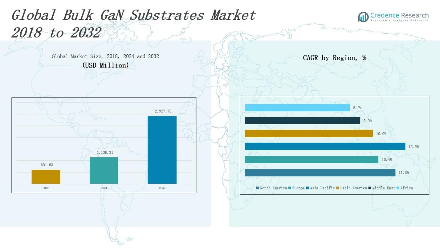
The Bulk GaN Substrates Market size was valued at USD 601.63 million in 2018 to USD 1,136.21 million in 2024 and is anticipated to reach USD 2,927.78 million by 2032, at a CAGR of 11.70% during the forecast period.
| REPORT ATTRIBUTE |
DETAILS |
| Historical Period |
2020-2024 |
| Base Year |
2024 |
| Forecast Period |
2025-2032 |
| Bulk GaN Substrates Market Size 2024 |
USD 1,136.21 Million |
| Bulk GaN Substrates Market, CAGR |
11.70% |
| Bulk GaN Substrates Market Size 2032 |
USD 2,927.78 Million |
The Bulk GaN Substrates Market is driven by rising demand for high-efficiency power electronics in electric vehicles, 5G infrastructure, and renewable energy systems. GaN’s superior thermal conductivity, breakdown voltage, and switching speed support its adoption over traditional silicon-based substrates. Increasing investments in wide-bandgap semiconductor research and advancements in vertical device architectures fuel market growth. Trends include miniaturization of power devices, expansion of GaN use in radar and satellite communication, and growing preference for native GaN substrates over epitaxial alternatives to enhance performance and reliability in high-frequency, high-power applications across industrial and defense sectors.
The Bulk GaN Substrates Market spans key regions including North America, Europe, Asia Pacific, Latin America, the Middle East, and Africa. Asia Pacific holds the largest share due to strong semiconductor manufacturing in China, Japan, and South Korea. North America and Europe follow with advanced R&D and defense applications. Latin America, the Middle East, and Africa show gradual growth. Key players include HexaTech, Inc., Kyma Technologies, NGK Insulators, Ltd., Cree, Inc. (Wolfspeed), Sumitomo Electric Industries, Mitsubishi Chemical Corporation, Saint-Gobain, Furukawa Co., Ltd., Ammono S.A., and Sino Nitride Semiconductor.
Access crucial information at unmatched prices!
Request your sample report today & start making informed decisions powered by Credence Research Inc.!
Download Sample
Market Insights
- The Bulk GaN Substrates Market was valued at USD 601.63 million in 2018, USD 1,136.21 million in 2024, and is projected to reach USD 2,927.78 million by 2032, growing at a CAGR of 11.70%.
- Rising demand for high-efficiency power devices in EVs, 5G networks, and renewable energy systems drives widespread adoption of native GaN substrates.
- Asia Pacific leads the market with over 40% share, followed by North America and Europe, supported by robust electronics manufacturing and strategic investments.
- The market faces cost and scalability challenges due to high-temperature, high-pressure GaN crystal fabrication and limited large-wafer availability.
- Key trends include vertical GaN device development, miniaturization of power components, and expanded GaN usage in radar and defense communication systems.
- North America and Europe benefit from defense and telecom demand, while Latin America, the Middle East, and Africa show gradual adoption growth.
- Major players include HexaTech, Cree (Wolfspeed), NGK Insulators, Kyma Technologies, Mitsubishi Chemical, Sumitomo Electric, Furukawa, and Sino Nitride Semiconductor.
Market Drivers
Growing Demand for High-Efficiency Power Devices Across Emerging Applications
The Bulk GaN Substrates Market benefits from rising adoption of high-efficiency power devices in electric vehicles, consumer electronics, and data centers. These substrates enable superior performance by reducing energy losses and allowing faster switching speeds compared to traditional silicon. EV manufacturers favor GaN for compact onboard chargers and power inverters. It meets efficiency mandates and supports thermal management under demanding conditions. Increasing power density requirements continue to push demand for high-quality GaN substrates across industries.
For instance, the EMOTION project developed GaN-based onboard chargers for electric vehicles, which are smaller, lighter, and offer higher efficiency and power density than silicon-based chargers, contributing to improved vehicle design and reduced energy dissipation.
Expansion of 5G Infrastructure and High-Frequency Communications
The global rollout of 5G networks strongly supports the Bulk GaN Substrates Market. GaN’s high electron mobility and frequency response make it ideal for RF power amplifiers in base stations and satellite systems. Telecom equipment manufacturers leverage bulk GaN substrates to build smaller, more powerful devices with improved heat dissipation. It enables better bandwidth, reduced latency, and extended device life. Growth in advanced radar and millimeter-wave systems also fuels market expansion.
For instance, Nokia has integrated GaN-based RF power amplifiers in its AirScale baseband solutions to boost signal efficiency and enable higher data throughput in 5G infrastructure.
Rising Investment in Wide-Bandgap Semiconductor Research and Manufacturing
Governments and private enterprises are investing heavily in wide-bandgap semiconductor R&D, which directly impacts the Bulk GaN Substrates Market. Strategic funding supports pilot production lines, equipment upgrades, and cleanroom facilities tailored for GaN processing. It accelerates commercial readiness and encourages new players to enter the supply chain. Focus on vertical integration strengthens quality control and cost efficiency. These investments drive volume growth and performance improvements in GaN-based electronic systems.
Increased Preference for Native GaN Substrates to Improve Device Performance
Device manufacturers increasingly prefer native GaN substrates over foreign alternatives like silicon or sapphire due to lattice matching and thermal compatibility advantages. The Bulk GaN Substrates Market gains from this shift, enabling lower defect density and improved reliability in power and RF devices. It helps eliminate performance bottlenecks in high-stress environments such as aerospace and defense. Demand rises for vertical GaN devices, which require bulk substrates for optimal current handling and scalability.
Market Trends
Shift Toward Native GaN Substrates for Superior Device Efficiency
The Bulk GaN Substrates Market reflects a strong shift toward native GaN substrates due to their superior crystal quality, reduced defect density, and better thermal management. These substrates enable higher current densities and enhanced reliability in high-power and high-frequency devices. Manufacturers prioritize native GaN to avoid performance limitations linked to heteroepitaxial growth on foreign substrates. It allows better lattice matching and electrical conductivity, supporting long-term device stability. This trend continues gaining traction in power and RF applications.
For instance, Furukawa Electric introduced bulk GaN wafers using Hydride Vapor Phase Epitaxy (HVPE) with improved thermal conductivity, reducing junction temperatures in high-power amplifiers.
Rising Adoption in Electric Vehicles and Power Electronics
Electric vehicle manufacturers increasingly adopt GaN substrates to reduce system size, weight, and power loss in inverters and onboard chargers. The Bulk GaN Substrates Market grows as OEMs and Tier 1 suppliers invest in GaN-based solutions for better power conversion and energy efficiency. It supports fast-charging infrastructure and thermal control in high-voltage systems. Demand for smaller, cooler, and more efficient power modules aligns with this trend across automotive and industrial sectors.
For instance, ROHM and TSMC have formed a strategic partnership to develop and mass-produce 650V GaN high-electron mobility transistors (HEMT) used in EV onboard chargers and inverters, with ROHM applying TSMC’s GaN-on-silicon process technology to enhance power device performance and sustainability for automotive uses.
Advancement in Vertical GaN Device Architectures
Technological progress in vertical GaN devices is a key trend shaping the Bulk GaN Substrates Market. Vertical architectures allow higher current throughput and voltage operation while minimizing chip area. It improves heat dissipation and performance in high-power systems, such as data centers and renewable energy inverters. Bulk GaN substrates enable these designs by offering thick, defect-free layers necessary for vertical transport. Device makers increasingly explore these structures to enhance integration and power density.
Integration with RF and Millimeter-Wave Technologies for 5G and Beyond
The Bulk GaN Substrates Market benefits from increased integration of GaN substrates in RF and millimeter-wave technologies for 5G, satellite communications, and radar systems. GaN’s wide bandgap and high-frequency response make it essential for next-gen telecommunication infrastructure. It enables miniaturization and efficiency in RF front-end modules. Growing deployment of phased-array antennas and beamforming technologies continues to drive demand. Manufacturers focus on developing high-purity substrates for scalable RF power solutions.
Market Challenges Analysis
High Manufacturing Costs and Limited Commercial Scalability
The Bulk GaN Substrates Market faces significant cost-related barriers due to complex fabrication processes and low material yields. Producing defect-free native GaN crystals requires high-pressure, high-temperature conditions, increasing capital and operational expenses. It remains difficult to scale substrate production while maintaining quality and affordability. These cost constraints hinder widespread adoption, especially in price-sensitive applications. Market participants struggle to balance performance benefits with economic viability, slowing broader commercialization efforts.
Technical Limitations in Wafer Size and Crystal Defect Management
The market also grapples with challenges related to wafer size limitations and persistent crystal defects. Most bulk GaN substrates are limited to smaller diameters compared to silicon, affecting throughput and device integration efficiency. It reduces compatibility with existing semiconductor fabrication tools optimized for larger wafers. Managing dislocation densities and surface imperfections remains a technical hurdle that impacts device performance and yield. These issues constrain the Bulk GaN Substrates Market from reaching mass production and full-scale industrial integration.
Market Opportunities
Expansion of Electric Mobility and Renewable Energy Infrastructure
The global push toward electric mobility and clean energy opens strong growth avenues for the Bulk GaN Substrates Market. Governments and manufacturers invest in electric vehicles, charging stations, and solar inverters, all of which benefit from GaN’s power efficiency. It enables compact, thermally stable, and high-performance systems ideal for these emerging applications. Bulk GaN substrates support fast-switching devices that improve energy conversion. The shift from silicon to GaN in power electronics unlocks new deployment scenarios.
Increased Demand for High-Frequency RF Devices in Advanced Communications
Rapid expansion in 5G, satellite internet, and defense communication networks drives demand for high-frequency RF devices, fueling opportunities in the Bulk GaN Substrates Market. GaN substrates offer the thermal and electrical performance needed for next-generation RF front ends and phased array antennas. It supports miniaturization and performance consistency in demanding environments. Market players can tap into aerospace, radar, and telecom sectors seeking reliable GaN-based components. Strategic investment in substrate quality and wafer scaling can enhance competitive positioning.
Market Segmentation Analysis:
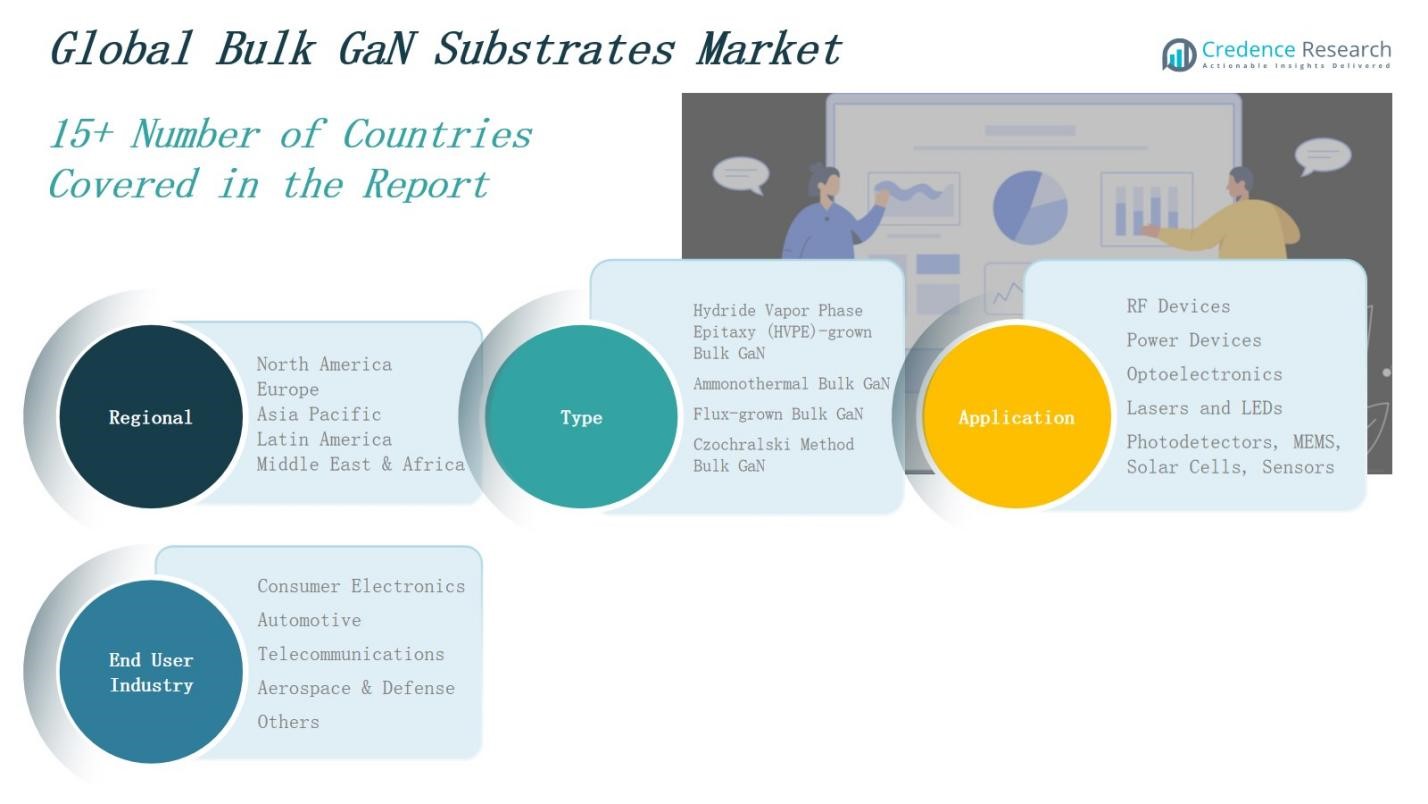
By Type
The Bulk GaN Substrates Market segments by type into Hydride Vapor Phase Epitaxy (HVPE)-grown, Ammonothermal, Flux-grown, and Czochralski Method Bulk GaN. HVPE-grown substrates hold a major share due to their scalability and relatively lower production cost. Ammonothermal GaN gains traction for delivering superior crystal quality and low dislocation density, making it suitable for high-performance devices. Flux-grown and Czochralski methods remain niche but support research-grade and specialty applications where uniformity and crystal perfection are critical.
For instance, Kyma Technologies has developed HVPE-grown GaN substrates that are used in commercial power electronics for their cost-effective production and high material integrity.
By Application
The Bulk GaN Substrates Market categorizes applications into RF Devices, Power Devices, Optoelectronics, Lasers and LEDs, and Photodetectors, MEMS, Solar Cells, and Sensors. RF devices dominate usage, driven by 5G base stations and satellite communication systems. Power devices follow closely, with GaN substrates enabling higher efficiency in EVs, chargers, and energy conversion systems. Optoelectronics and laser applications benefit from high-frequency operation and thermal stability. Sensors and photodetectors see growing use in aerospace, defense, and industrial automation.
For instance, Raytheon Technologies uses GaN-based RF devices in its AN/APG-79 radar for enhanced range and target detection in fighter aircraft.
By End User Industry
End users in the Bulk GaN Substrates Market include Consumer Electronics, Automotive, Telecommunications, Aerospace & Defense, and Others. The telecommunications sector leads demand due to the rise of high-frequency RF devices in mobile networks. Automotive companies invest in GaN-based inverters and converters to meet efficiency and size requirements in EV platforms. Aerospace and defense utilize GaN substrates for radar, communication, and power systems. Consumer electronics and emerging sectors contribute to long-term market expansion.
Segments:
Based on Type
- Hydride Vapor Phase Epitaxy (HVPE)-grown Bulk GaN
- Ammonothermal Bulk GaN
- Flux-grown Bulk GaN
- Czochralski Method Bulk GaN
Based on Application
- RF Devices
- Power Devices
- Optoelectronics
- Lasers and LEDs
- Photodetectors, MEMS, Solar Cells, Sensors
Based on End User Industry
- Consumer Electronics
- Automotive
- Telecommunications
- Aerospace & Defense
- Others
Based on Region:
- North America
- Europe
- Germany
- France
- U.K.
- Italy
- Spain
- Rest of Europe
- Asia Pacific
- China
- Japan
- India
- South Korea
- South-east Asia
- Rest of Asia Pacific
- Latin America
- Brazil
- Argentina
- Rest of Latin America
- Middle East & Africa
- GCC Countries
- South Africa
- Rest of the Middle East and Africa
Regional Analysis
North America
The North America Bulk GaN Substrates Market size was valued at USD 172.27 million in 2018 to USD 320.19 million in 2024 and is anticipated to reach USD 828.58 million by 2032, at a CAGR of 11.8% during the forecast period. The region holds over 28% of the global market share, driven by strong demand from aerospace, defense, and telecom sectors. It benefits from advanced R&D infrastructure, semiconductor manufacturing capabilities, and adoption of GaN in 5G and power applications. The U.S. leads regional growth with increased investment in high-frequency RF devices and military-grade GaN systems. Canada and Mexico contribute through automotive and industrial electronics. The market remains competitive with presence of major players and favorable policy support.
Europe
The Europe Bulk GaN Substrates Market size was valued at USD 117.79 million in 2018 to USD 210.83 million in 2024 and is anticipated to reach USD 496.41 million by 2032, at a CAGR of 10.4% during the forecast period. Europe accounts for approximately 18% of the global market share. Germany, France, and the UK drive growth through demand in EV power electronics, industrial automation, and radar systems. It sees robust expansion in energy-efficient technologies supported by EU green energy policies. Companies focus on GaN for power conversion and RF applications. Ongoing collaborations between research institutions and semiconductor firms strengthen regional innovation.
Asia Pacific
The Asia Pacific Bulk GaN Substrates Market size was valued at USD 259.51 million in 2018 to USD 508.43 million in 2024 and is anticipated to reach USD 1,391.04 million by 2032, at a CAGR of 12.5% during the forecast period. Asia Pacific dominates the global market with a share exceeding 40%. China, Japan, and South Korea lead adoption due to strong electronics and automotive manufacturing ecosystems. It benefits from large-scale investments in 5G infrastructure, electric mobility, and semiconductor fabs. Taiwan and India also expand contributions through government-led manufacturing incentives. The region offers low-cost manufacturing and rapid commercialization of GaN technologies.
Latin America
The Latin America Bulk GaN Substrates Market size was valued at USD 28.42 million in 2018 to USD 53.00 million in 2024 and is anticipated to reach USD 120.88 million by 2032, at a CAGR of 10.0% during the forecast period. Latin America holds nearly 4% of the global market. Brazil leads regional growth with adoption of GaN in power systems, telecom equipment, and industrial applications. Mexico supports demand through its electronics and automotive supply chains. The market gains from gradual digital infrastructure upgrades and increased interest in renewable energy integration. Regional innovation remains limited but is improving through partnerships with global tech firms.
Middle East
The Middle East Bulk GaN Substrates Market size was valued at USD 15.18 million in 2018 to USD 25.94 million in 2024 and is anticipated to reach USD 55.12 million by 2032, at a CAGR of 9.0% during the forecast period. The region accounts for about 2% of global market share. It shows rising demand in military communication, satellite, and radar systems. Gulf countries invest in defense modernization and smart grid infrastructure. Israel contributes significantly with advanced semiconductor R&D and niche RF applications. The market shows potential but requires greater manufacturing capabilities and policy alignment for long-term scaling.
Africa
The Africa Bulk GaN Substrates Market size was valued at USD 8.46 million in 2018 to USD 17.82 million in 2024 and is anticipated to reach USD 35.74 million by 2032, at a CAGR of 8.2% during the forecast period. Africa holds less than 1.5% of the global market. South Africa leads regional activity, driven by telecom upgrades and university-led research. Egypt and Nigeria show early interest in GaN-based systems for energy and connectivity. The market remains nascent due to limited local manufacturing and high import dependency. It requires strategic partnerships and technology transfer to unlock wider adoption and innovation.
Shape Your Report to Specific Countries or Regions & Enjoy 30% Off!
Key Player Analysis
- HexaTech, Inc.
- Kyma Technologies
- NGK Insulators, Ltd.
- Furukawa Co., Ltd.
- Saint-Gobain
- Cree, Inc. (Wolfspeed)
- Ammono S.A.
- Sino Nitride Semiconductor
- Mitsubishi Chemical Corporation
- Sumitomo Electric Industries, Ltd.
Competitive Analysis
The Bulk GaN Substrates Market features a concentrated competitive landscape dominated by a mix of established materials companies and specialized semiconductor firms. Key players include HexaTech, Inc., Kyma Technologies, NGK Insulators, Ltd., and Cree, Inc. (Wolfspeed), all of which focus on native GaN substrate development with advanced crystal growth techniques. It attracts investment from vertically integrated manufacturers like Sumitomo Electric Industries, Ltd. and Mitsubishi Chemical Corporation that leverage in-house capabilities to support scale and quality. Players compete on purity, dislocation density, wafer diameter, and cost efficiency. Companies such as Saint-Gobain and Furukawa Co., Ltd. emphasize R&D to improve yield and thermal performance. Strategic partnerships, IP portfolios, and regional expansion remain key to sustaining market share. The Bulk GaN Substrates Market continues to evolve as firms target applications in power electronics, RF systems, and optoelectronics, creating opportunities for innovation and differentiation through proprietary technologies and customized substrate solutions.
Recent Developments
- In April 2025, Sanken Electric Co., Ltd. acquired Powdec K.K. to enhance its expertise in GaN-on-GaN epitaxial wafer production and strengthen its capabilities in bulk GaN crystal growth technologies.
- In July 2025, Navitas Semiconductor partnered with Powerchip Semiconductor Manufacturing Corporation (PSMC) to launch 200 mm GaN-on-Si production in Taiwan, supporting high-volume manufacturing for EVs, AI data centers, and solar energy systems.
- In January 2025, Toyoda Gosei announced advancements in GaN substrate technology, demonstrating improved device performance using GaN seed crystal-based substrates, as published in Physica Status Solidi.
- In May 2024, Power Integrations acquired Odyssey Semiconductor, gaining access to bulk GaN substrate capabilities to support its vertical integration strategy for GaN device manufacturing.
Market Concentration & Characteristics
The Bulk GaN Substrates Market exhibits moderate to high market concentration, with a limited number of specialized players controlling a significant share. It is characterized by high entry barriers due to complex crystal growth processes, capital-intensive equipment, and stringent quality requirements. Leading companies invest heavily in R&D to improve substrate purity, reduce defect density, and scale wafer sizes. The market focuses on vertically integrated supply chains to ensure consistency and cost efficiency. It demands expertise in wide-bandgap semiconductor technology and advanced epitaxial techniques. Strategic partnerships and intellectual property portfolios strengthen competitive positions. The Bulk GaN Substrates Market continues to evolve through innovation in vertical device structures and native GaN production. Demand for customized, high-performance substrates supports premium pricing models. Growth remains concentrated in key application areas such as RF power devices, EV systems, and satellite communications. Regional dynamics and technological capability strongly influence the competitive landscape and innovation pipeline.
Report Coverage
The research report offers an in-depth analysis based on Type, Application, End-User Industry and Region. It details leading market players, providing an overview of their business, product offerings, investments, revenue streams, and key applications. Additionally, the report includes insights into the competitive environment, SWOT analysis, current market trends, as well as the primary drivers and constraints. Furthermore, it discusses various factors that have driven market expansion in recent years. The report also explores market dynamics, regulatory scenarios, and technological advancements that are shaping the industry. It assesses the impact of external factors and global economic changes on market growth. Lastly, it provides strategic recommendations for new entrants and established companies to navigate the complexities of the market.
Future Outlook
- Demand for native GaN substrates will grow with increased adoption in high-power and high-frequency applications.
- Vertical GaN devices will drive the need for thicker, low-defect bulk substrates.
- Electric vehicle systems will expand usage of GaN substrates in onboard chargers and power inverters.
- RF and millimeter-wave devices will continue to support growth in telecom and satellite sectors.
- Investments in GaN fabrication facilities will enhance global supply chain stability.
- Wafer size scalability will become a competitive differentiator among leading manufacturers.
- Research in defect reduction and thermal performance will improve substrate quality.
- Strategic partnerships between semiconductor firms and OEMs will increase customized substrate development.
- Asia Pacific will maintain its dominance due to advanced manufacturing infrastructure and strong demand.
- Government support for wide-bandgap semiconductors will accelerate commercialization and innovation efforts.


