Market Overview:
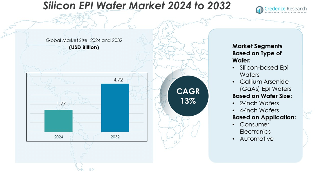
Silicon EPI Wafer Market size was valued USD 1.77 billion in 2024 and is anticipated to reach USD 4.72 billion by 2032, at a CAGR of 13% during the forecast period.
| REPORT ATTRIBUTE |
DETAILS |
| Historical Period |
2020-2023 |
| Base Year |
2024 |
| Forecast Period |
2025-2032 |
| Silicon EPI Wafer Market Size 2024 |
USD 1.77 billion |
| Silicon EPI Wafer Market, CAGR |
13% |
| Silicon EPI Wafer Market Size 2032 |
USD 4.72 billion |
The silicon EPI wafer market features strong competition among top players, including SUMCO Corporation, Sumitomo Electric Industries, Ltd., IQE plc, Epistar Corporation, JA Solar Holdings, Co., Ltd., Jinko Solar Holding Co., Ltd., LONGi Green Energy Technology Co Ltd, GCL-Poly Energy Holdings Limited, Topsil Semiconductor Materials A/S, and NanoSystec GmbH. These companies focus on expanding wafer sizes, advancing epitaxy technologies, and strengthening supply chains to meet growing demand from electronics, automotive, and renewable energy sectors. Asia-Pacific leads the global market with a 46% share, driven by its dominance in semiconductor manufacturing, strong presence of leading foundries, and large-scale consumer electronics demand, positioning it as the fastest-growing regional hub.
Market Insights
- The Silicon EPI Wafer Market size was USD 1.77 billion in 2024 and will reach USD 4.72 billion by 2032, growing at a CAGR of 13%.
- Rising demand from consumer electronics and electric vehicles drives adoption, with silicon-based epi wafers holding over 45% share due to cost efficiency and wide application.
- Key players including SUMCO, Sumitomo Electric, IQE, Epistar, JA Solar, Jinko Solar, LONGi, GCL-Poly, Topsil, and NanoSystec compete by advancing wafer sizes, improving epitaxy quality, and expanding global supply chains.
- High manufacturing costs and limited availability of wide-bandgap materials like SiC and GaN wafers remain restraints, challenging smaller producers and adding pressure on profitability.
- Asia-Pacific leads the global market with 46% share, supported by strong semiconductor manufacturing in China, Taiwan, Japan, and South Korea, while North America holds 24% share and Europe 19%, reflecting demand from automotive, defense, and renewable energy sectors.
Access crucial information at unmatched prices!
Request your sample report today & start making informed decisions powered by Credence Research Inc.!
Download Sample
Market Segmentation Analysis:
By Type of Wafer
The silicon-based epi wafer segment dominates the market with over 45% share, driven by its extensive use in consumer electronics, automotive, and telecommunications. These wafers offer high compatibility with existing semiconductor manufacturing processes, making them the most widely adopted. Gallium arsenide (GaAs) and silicon carbide (SiC) epi wafers are gaining traction for their superior performance in high-frequency and high-power applications, while gallium nitride (GaN) wafers continue to expand in RF and 5G markets. However, silicon-based epi wafers maintain dominance due to cost efficiency and mature supply chains.
- For instance, JA Solar operates wafer production facilities with an annual capacity exceeding 100 GW, enabling large-scale integration into its downstream solar cell and module lines. The company has invested heavily in capacity expansion to support this vertical integration strategy.
By Wafer Size
The 12-inch wafer segment holds the largest market share, exceeding 50%, as it supports high-volume semiconductor manufacturing and offers better cost efficiency per chip. Its adoption is fueled by leading foundries and integrated device manufacturers focusing on advanced nodes and large-scale production. While 8-inch wafers remain relevant for mature technologies in automotive and industrial sectors, smaller sizes like 4-inch and 6-inch wafers serve niche applications in research and specialty devices. The transition toward larger wafer formats continues to be driven by demand for higher yields, reduced production costs, and advanced fabrication processes.
- For instance, Epistar has developed an 8-inch GaN-on-silicon epiwafer for Micro-LED displays, and also a 6-inch chip-on-wafer (COW) Micro-LED structure, enabling tighter pixel pitch and higher panel yield.
By Application
Consumer electronics represent the leading application segment, capturing over 35% share, driven by the high demand for smartphones, tablets, and wearable devices. The growth of AI chips, high-performance processors, and memory solutions further boosts adoption. Automotive applications are growing rapidly with the rise of electric vehicles and advanced driver-assistance systems, where SiC and GaN wafers play critical roles. Industrial and telecommunications sectors also contribute significantly, especially with the expansion of 5G networks and IoT devices. Healthcare and defense applications remain emerging, supported by innovations in sensors, imaging, and secure communication systems.
Market Overview
Rising Demand for Consumer Electronics
The growing demand for smartphones, tablets, and wearable devices continues to drive the silicon epi wafer market. Silicon-based epi wafers remain central to producing high-performance chips required for advanced displays, memory, and processors. With 5G adoption and AI-enabled devices gaining momentum, manufacturers increasingly rely on wafers that deliver higher efficiency and reliability. Expanding applications in OLED panels, high-speed processors, and compact electronics ensure consistent demand, reinforcing the dominance of silicon-based wafers in the consumer electronics segment.
- For instance, NanoSystec provides active alignment modules achieving < 100 nm precision in opto-electronic coupling, and positioning systems with < 1 µm placement tolerance, which support integration of epi-based photonic and MEMS components into consumer devices.
Expansion of Electric Vehicles and Automotive Electronics
The rapid growth of electric vehicles (EVs) and advanced driver-assistance systems (ADAS) significantly boosts the need for epi wafers. Silicon carbide (SiC) and gallium nitride (GaN) epi wafers are particularly critical, offering high thermal conductivity and superior power handling for EV inverters and charging systems. Automakers are partnering with wafer suppliers to secure stable supply chains, supporting large-scale adoption. As governments push for cleaner mobility and automakers accelerate EV production, epi wafers are positioned as an essential material in the automotive electronics ecosystem.
- For instance, Jinko Solar’s subsidiary Jiangxi Jinko plans to build 56 GW of annual capacity—including in silicon wafers and ingesting materials—ensuring supply to downstream power electronics and module lines.
Advancements in Semiconductor Manufacturing Technologies
Ongoing innovation in semiconductor manufacturing, such as scaling to advanced nodes and integration of 3D structures, drives the adoption of epi wafers. Larger wafer formats like 12-inch enhance yields and reduce costs, enabling mass production of complex chips. Advanced epitaxy techniques ensure uniformity, defect reduction, and high performance in next-generation devices. These advancements support applications in AI, data centers, and 5G infrastructure. The continuous push for smaller, faster, and more energy-efficient semiconductors ensures sustained demand for epi wafers across industries.
Key Trends & Opportunities
Adoption of Wide-Bandgap Materials
The shift toward wide-bandgap materials, including SiC and GaN epi wafers, presents strong growth opportunities. These materials deliver superior performance in high-power and high-frequency applications compared to traditional silicon. Industries such as automotive, telecommunications, and renewable energy increasingly adopt them for EV powertrains, 5G base stations, and efficient power conversion systems. Their ability to operate at higher voltages and temperatures makes them attractive for next-generation electronics, positioning them as a transformative trend within the epi wafer landscape.
- For instance, LONGi’s TaiRay silicon wafers reduce resistivity variation along the ingot axis from ~3× to within 1.5× between head and tail through refined RCz growth.
Growing Role of 5G and IoT Applications
The global rollout of 5G networks and the rising adoption of IoT devices are creating significant opportunities for epi wafer demand. Gallium arsenide (GaAs) and GaN epi wafers enable high-frequency, low-loss performance crucial for 5G base stations, antennas, and IoT sensors. As smart cities and connected infrastructure expand, the demand for advanced semiconductors capable of supporting large data flows and high connectivity intensifies. This trend underscores the increasing importance of epi wafers in driving next-generation communication technologies.
- For instance, Sumitomo Electric has expanded its GaN-on-SiC epitaxial wafer production to the 150 mm (6-inch) scale, upgrading from 4-inch lines to enable higher yield and reduced cost for RF devices.
Key Challenges
High Manufacturing Costs and Complexity
Epi wafer production involves complex epitaxial growth processes that require advanced equipment, controlled environments, and significant capital investment. This leads to high manufacturing costs, which challenge profitability, especially for smaller players. Wide-bandgap materials like SiC and GaN are even more expensive due to intricate production methods and limited availability of substrates. Balancing cost efficiency with quality and scale remains a major challenge for manufacturers seeking to stay competitive in a market with rising demand across diverse applications.
Supply Chain Constraints and Limited Material Availability
The market faces persistent supply chain bottlenecks and limited availability of high-quality substrates, particularly for SiC and GaN wafers. Production capacity is concentrated among a few large suppliers, creating dependency risks for downstream industries such as automotive and electronics. Shortages can delay production schedules, inflate costs, and hinder market expansion. Securing a consistent and diversified supply of raw materials remains a pressing challenge, especially as demand accelerates in EVs, renewable energy, and advanced semiconductor applications worldwide.
Regional Analysis
North America
North America holds a 24% share of the silicon EPI wafer market, driven by strong demand from consumer electronics, data centers, and defense applications. The U.S. leads the region with extensive investments in semiconductor R&D and manufacturing capacity expansions. The presence of major technology companies accelerates adoption of advanced wafers for AI, 5G, and automotive electronics. Government support for domestic semiconductor manufacturing under initiatives like the CHIPS Act further strengthens the regional market. Canada and Mexico contribute moderately, with growth led by industrial and automotive applications, reinforcing North America’s position as a key innovation hub.
Europe
Europe accounts for 19% of the market, with Germany, France, and the U.K. as primary contributors. The region’s demand is fueled by automotive electronics, renewable energy systems, and industrial automation. Germany dominates with its leadership in electric vehicles and advanced automotive technologies, driving demand for SiC and GaN epi wafers. France and the U.K. support growth through investments in telecommunications and defense applications. The European Union’s focus on reducing dependency on Asian semiconductor imports and promoting local manufacturing boosts adoption. Europe’s market share reflects its focus on high-performance, sustainable, and energy-efficient semiconductor technologies.
Asia-Pacific
Asia-Pacific leads the silicon EPI wafer market with a commanding 46% share, anchored by China, Japan, South Korea, and Taiwan. The region benefits from its role as the global semiconductor manufacturing hub, supported by advanced foundries and large-scale consumer electronics demand. China drives growth with government-backed investments in domestic chip production, while Taiwan and South Korea dominate in memory and logic chip fabrication. Japan contributes through innovation in materials and epitaxy technologies. Strong demand from automotive, 5G, and industrial applications solidifies Asia-Pacific’s leadership, making it the largest and fastest-growing regional market for epi wafers.
Latin America
Latin America holds a smaller 6% share of the global silicon EPI wafer market, primarily driven by Brazil and Mexico. Growth in the region is supported by expanding electronics manufacturing, renewable energy projects, and adoption of smart infrastructure. Brazil leads with demand for industrial automation and telecommunications, while Mexico’s role as a manufacturing hub for North American automotive supply chains supports wafer demand. Limited domestic semiconductor production remains a challenge, with reliance on imports from Asia-Pacific and North America. Despite its modest share, the region shows growth potential as technology adoption and industrialization accelerate.
Middle East & Africa
The Middle East & Africa region captures 5% of the silicon EPI wafer market, led by the UAE, Saudi Arabia, and South Africa. Growing investments in telecommunications infrastructure, particularly 5G rollout, drive demand for advanced wafers. The defense and aerospace industries in the Middle East also create opportunities for high-performance semiconductor applications. In Africa, South Africa contributes through industrial and healthcare sectors adopting advanced electronics. Although the region’s semiconductor manufacturing base is limited, increasing investments in smart cities, renewable energy, and digital transformation support steady growth, positioning MEA as an emerging opportunity in the global market.
Market Segmentations:
By Type of Wafer:
- Silicon-based Epi Wafers
- Gallium Arsenide (GaAs) Epi Wafers
By Wafer Size:
- 2-inch Wafers
- 4-inch Wafers
By Application:
- Consumer Electronics
- Automotive
By Geography
- North America
- Europe
- UK
- France
- Germany
- Italy
- Spain
- Russia
- Belgium
- Netherlands
- Austria
- Sweden
- Poland
- Denmark
- Switzerland
- Rest of Europe
- Asia Pacific
- China
- Japan
- South Korea
- India
- Australia
- Thailand
- Indonesia
- Vietnam
- Malaysia
- Philippines
- Taiwan
- Rest of Asia Pacific
- Latin America
- Brazil
- Argentina
- Peru
- Chile
- Colombia
- Rest of Latin America
- Middle East
- UAE
- KSA
- Israel
- Turkey
- Iran
- Rest of Middle East
- Africa
- Egypt
- Nigeria
- Algeria
- Morocco
- Rest of Africa
Competitive Landscape
The silicon EPI wafer market players such as JA Solar Holdings, Co., Ltd., Epistar Corporation, NanoSystec GmbH, Jinko Solar Holding Co., Ltd., SUMCO Corporation, LONGi Green Energy Technology Co Ltd, Topsil Semiconductor Materials A/S, IQE plc, GCL-Poly Energy Holdings Limited, and Sumitomo Electric Industries, Ltd. The silicon EPI wafer market is highly competitive, characterized by continuous innovation, capacity expansions, and strategic partnerships. Companies are investing in advanced epitaxy techniques to improve wafer quality, reduce defect density, and enable higher performance for next-generation semiconductors. The shift toward wide-bandgap materials such as silicon carbide and gallium nitride has intensified competition, as demand rises in electric vehicles, 5G infrastructure, and renewable energy systems. Market players also focus on scaling 12-inch wafer production to enhance yields and cost efficiency. Additionally, collaborations with foundries and device manufacturers strengthen supply chains, ensuring reliable delivery of high-quality wafers worldwide.
Shape Your Report to Specific Countries or Regions & Enjoy 30% Off!
Key Player Analysis
- JA Solar Holdings, Co., Ltd.
- Epistar Corporation
- NanoSystec GmbH
- Jinko Solar Holding Co., Ltd.
- SUMCO Corporation
- LONGi Green Energy Technology Co Ltd
- Topsil Semiconductor Materials A/S
- IQE plc
- GCL-Poly Energy Holdings Limited
- Sumitomo Electric Industries, Ltd.
Recent Developments
- In November 2024, ZMC announced the acquisition of Pure Wafer PLC to undertake a new growth phase with substantial investments in capacity expansion across its U.S. wafer operations, including advanced technology and tooling to meet the demand of top semiconductor original equipment makers (OEMs) and the semiconductor integrated device manufacturers (IDMs) they serve.
- In April 2024, Adani Group initiated commercial production of wafers and ingots essential for solar power cells at its facility in Gujarat. This move is part of a broader strategy to enhance its renewable energy capabilities, aiming to generate 45 gigawatts (GW) of renewable power by 2030, with a significant portion coming from its Khavda Renewable Energy Park in Gujarat.
- In March 2024, Siltronic announced plans to gradually cease production of small-diameter wafers at its Burghausen site in Germany, citing changing industry demands and the end of the product life cycle.
- In June 2023, American wafer fabrication manufacturer Lam Research developed Coronus DX. It can deposit a proprietary protective film coating on both sides of the wafer edge in a single step, preventing damage and defects frequently occurring during advanced semiconductor manufacturing
Report Coverage
The research report offers an in-depth analysis based on Type of Wafer, Wafer Size, Application and Geography. It details leading market players, providing an overview of their business, product offerings, investments, revenue streams, and key applications. Additionally, the report includes insights into the competitive environment, SWOT analysis, current market trends, as well as the primary drivers and constraints. Furthermore, it discusses various factors that have driven market expansion in recent years. The report also explores market dynamics, regulatory scenarios, and technological advancements that are shaping the industry. It assesses the impact of external factors and global economic changes on market growth. Lastly, it provides strategic recommendations for new entrants and established companies to navigate the complexities of the market.
Future Outlook
- The demand for silicon epi wafers will rise with expanding consumer electronics adoption.
- Electric vehicles will drive significant growth for SiC and GaN epi wafers.
- 5G network expansion will boost demand for high-frequency epi wafers.
- Larger wafer sizes will dominate production to improve yields and cost efficiency.
- Renewable energy applications will create new opportunities for epi wafer suppliers.
- Semiconductor innovation will accelerate adoption of advanced epitaxy technologies.
- Strategic partnerships will strengthen global supply chain resilience.
- Investments in local semiconductor manufacturing will reduce regional import dependency.
- Emerging applications in healthcare and aerospace will support steady demand.
- Asia-Pacific will maintain market leadership with strong manufacturing capabilities.