Market Overview:
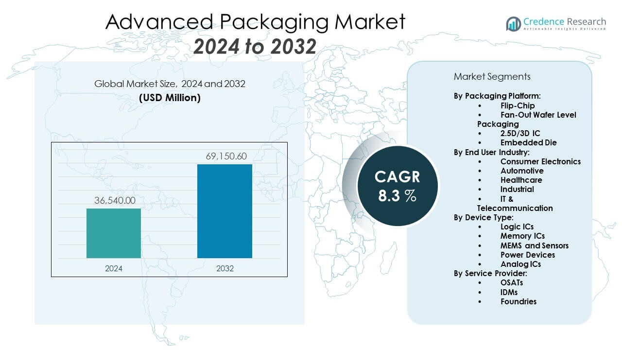
The Advanced Packaging Market is projected to grow from USD 36,540 million in 2024 to USD 69,150.6 million by 2032, registering a CAGR of 8.3% during the forecast period.
| REPORT ATTRIBUTE |
DETAILS |
| Historical Period |
2020-2024 |
| Base Year |
2024 |
| Forecast Period |
2025-2032 |
| Advanced Packaging Market Size 2024 |
USD 36,540 Million |
| Advanced Packaging Market, CAGR |
8.3% |
| Advanced Packaging Market Size 2032 |
USD 69,150.6 Million |
This growth is driven by increasing demand for compact, high-performance semiconductor devices to support advanced applications such as AI, 5G networks, and IoT. These technologies require sophisticated integration, leading to the rise of heterogeneous packaging, fan-out wafer-level packaging, and advanced node technologies. Leading foundries and outsourced semiconductor assembly and test (OSAT) providers are investing in innovative packaging solutions to support rising performance and miniaturization demands across smartphones, automotive electronics, and high-performance computing.
North America dominates the Advanced Packaging Market, backed by strong R&D infrastructure and leading semiconductor companies. Asia-Pacific is the largest manufacturing base, supported by robust semiconductor supply chains in China, Taiwan, and South Korea. These countries drive mass production and innovation through strategic investments in fabrication and assembly facilities. Europe holds steady growth, underpinned by demand in automotive and industrial electronics. Meanwhile, Latin America and the Middle East & Africa are witnessing early-stage development, with rising investments in electronics and telecom driving gradual market penetration. Overall, global momentum in digitalization and connectivity is shaping the future of advanced packaging technologies.
Access crucial information at unmatched prices!
Request your sample report today & start making informed decisions powered by Credence Research Inc.!
Download Sample
Market Insights:
- The Advanced Packaging Market is projected to grow from USD 36,540 million in 2024 to USD 69,150.6 million by 2032, reflecting rising demand for compact and high-performance chip packages.
- Miniaturization of devices and rising chip complexity are driving innovation in 2.5D/3D ICs, fan-out wafer-level packaging, and chiplet architectures.
- The surge in AI, 5G, and HPC applications fuels adoption of high-bandwidth and energy-efficient packaging solutions.
- Material shortages, high CapEx, and complex testing requirements pose challenges to scalability and new player entry.
- Asia-Pacific dominates the global market, while North America and Europe show growth in HPC and automotive segments respectively.
- Sustainability and ESG compliance are influencing packaging material selection and process optimization across the industry.
- Partnerships among IDMs, OSATs, and foundries are reshaping the packaging landscape to meet emerging electronic device demands.
Market Drivers:
Rising Demand for Miniaturization:
Manufacturers increasingly prioritize chip miniaturization without sacrificing performance. Advanced Packaging Market solutions such as 2.5D and 3D integration enable reduced footprint and higher I/O density. Demand for compact devices in wearables, smartphones, and medical sensors drives advanced interconnect technologies. These packaging formats address thermal dissipation, bandwidth limitations, and power efficiency. Foundries are adopting chiplets and die-to-die interconnects to meet these design complexities. Packaging becomes a vital enabler of Moore’s Law continuation. The emphasis on dense, efficient designs strengthens market demand.
- For instance, TSMC’s System on Integrated Chips (SoIC) technology achieves sub-10μm die-to-die interconnect pitch—enabling high-density vertical stacking with higher bandwidth, improved power integrity, and energy efficiency compared with traditional packaging methods.
Surge in AI and HPC Applications:
The growing penetration of AI, machine learning, and high-performance computing (HPC) applications increases reliance on heterogeneous integration. The Advanced Packaging Market supports multi-chip module (MCM) solutions enabling diverse functionalities on a single package. This approach enhances computing speed, data throughput, and power management. The rise in demand for large-scale data centers and edge AI devices boosts interest in silicon interposers and EMIB technologies. High-performance GPUs and AI accelerators adopt these packages. Market players develop custom solutions to handle massive bandwidth and compute loads. Advanced packaging accelerates AI’s computational footprint.
- For instance, AMD’s EPYC “Bergamo” processor implements advanced chiplet packaging on TSMC’s 5nm process, integrating 128 Zen 4c cores and 82 billion transistors in one socket. This delivers top-tier core density for large-scale data centers and AI, with the highest vCPU density in its class.
Adoption of 5G and IoT Technologies:
5G rollout requires components that handle higher frequency bands and heat management. The Advanced Packaging Market delivers FO-WLP, RF-SiP, and antenna-in-package technologies suitable for 5G modules. These packaging methods improve signal integrity, lower latency, and maintain signal strength in compact devices. IoT proliferation amplifies the need for low-power, small form-factor packages. Connected sensors in smart homes, industrial automation, and healthcare depend on robust packaging. Packaging becomes essential for next-gen connectivity. Industry investments in mmWave, RF packaging, and edge computing continue rising to match telecom evolution.
Increased Investment by OSATs and Foundries:
Outsourced Semiconductor Assembly and Test (OSAT) providers and leading foundries invest in R&D and facility upgrades. The Advanced Packaging Market is influenced by innovations in wafer-level and fan-out packaging technologies. Collaborations between design houses, IDMs, and OSATs accelerate adoption of new standards. Investment in high-density substrate manufacturing and panel-level packaging is surging. Foundries integrate advanced packaging early in chip design cycles. The vertical collaboration improves customization and performance. These strategic moves help expand capabilities, reduce time-to-market, and enhance package reliability.
Market Trends:
Shift Toward Heterogeneous Integration:
Heterogeneous integration enables combining different technologies in a single package. Advanced Packaging Market supports this shift by facilitating 2.5D, 3D stacking, and chiplet-based designs. It helps integrate analog, logic, RF, and memory dies. The demand for compact, multifunctional devices drives interest in such integration. Foundries and IDMs are collaborating to create co-designed chip systems. This trend allows faster data transfer and power savings. It plays a pivotal role in AI, HPC, and autonomous applications. System-in-package and system-on-integrated-substrate approaches continue gaining traction.
- For instance, Intel’s Ponte Vecchio GPU utilizes Foveros 3D and EMIB 2.5D advanced packaging to integrate transistors across 47 active tiles on a single package, boosting computational and memory integration for exascale computing.
Rise in Fan-Out Packaging Adoption:
Fan-out wafer-level packaging (FOWLP) provides high performance with lower package height and improved thermal behavior. Advanced Packaging Market benefits from widespread FOWLP adoption across smartphones, wearables, and automotive electronics. It allows smaller package sizes and cost-effective designs. Manufacturers use chip-first and chip-last techniques to meet specific application needs. The ongoing demand for high-speed mobile and AI applications accelerates its deployment. It supports scalable, flexible production that aligns with next-gen device demands. OSATs are investing in panel-level fan-out solutions to enhance throughput and yield.
- For instance, Apple’s A10 and subsequent A-series application processors use TSMC’s Integrated Fan-Out (InFO) technology, resulting in up to 30% reduction in package thickness compared to conventional PoP solutions, alongside increased I/O density and improved thermal performance.
Increased Use of Embedded Die Technologies:
Embedded die packaging integrates active/passive components directly into the substrate or PCB. Advanced Packaging Market sees growing use of this technology in RF modules, power devices, and medical electronics. It enhances thermal management and reduces signal losses. Embedded packaging enables reduced z-height, making it ideal for compact electronics. Players in automotive and defense sectors embrace it for reliability. The method supports co-packaging of analog and digital components. It leads to reduced interconnect length and better electrical performance.
Sustainability in Packaging Processes:
Environmental regulations and ESG pressures push manufacturers toward greener packaging. Advanced Packaging Market firms adopt halogen-free laminates, lead-free bumps, and recyclable mold compounds. Eco-friendly processes minimize water and chemical usage. Efforts focus on eliminating hazardous materials from substrates and die attach methods. Equipment makers develop low-temperature bonding and solvent-free cleaning solutions. Packaging formats are evaluated for material efficiency and carbon impact. Manufacturers prioritize compliance with REACH and RoHS directives.
Market Challenges Analysis:
Complexity in Multi-Die Integration and Reliability Testing:
The Advanced Packaging Market faces design complexities with multi-die integration and advanced interconnect architectures. As chips become more compact and heterogeneous, issues with heat dissipation, signal integrity, and mechanical stress increase. The industry struggles with validating performance and long-term reliability. Advanced packages require highly customized test solutions, which increase cost and time-to-market. Additionally, failure analysis becomes more intricate due to the dense structure of 2.5D and 3D stacks. Market players must ensure consistent performance while scaling volumes. These engineering challenges hinder mainstream adoption among smaller firms.
High Capital Costs and Supply Chain Limitations:
Setting up advanced packaging lines demands substantial investment in wafer handling, lithography, and bonding tools. The Advanced Packaging Market contends with high operational expenses and a limited number of suppliers for critical materials such as ABF substrates and advanced laminates. Global disruptions expose the vulnerability of packaging ecosystems. Lead times for equipment and substrates stretch product development cycles. Smaller OSATs struggle to compete with larger peers who can scale rapidly. High capital intensity deters new entrants, while raw material costs remain volatile. These factors constrain innovation speed and mass deployment.
Market Opportunities:
Expansion in Automotive and Industrial Sectors:
The increasing electronic content in electric vehicles, autonomous systems, and smart factories opens new opportunities for the Advanced Packaging Market. Advanced systems require robust thermal and electrical performance, making advanced packaging ideal for power modules, sensors, and control units. The shift to EVs and ADAS drives demand for SiP and embedded packages. Industrial IoT deployments also need compact, durable packaging for harsh environments. These sectors prioritize reliability, long lifecycle, and high thermal thresholds. Market players focusing on automotive-grade substrates and packaging formats gain competitive advantage.
Advancements in 3D Stacking and Chiplet Architectures:
Chiplet-based design and 3D stacking are gaining momentum as alternatives to monolithic SoCs. The Advanced Packaging Market can capitalize on this transition by providing solutions like interposers, through-silicon vias (TSVs), and hybrid bonding. These technologies support integration of heterogeneous IP blocks, offering flexibility and scalability. Cloud computing, HPC, and AI chips benefit significantly from such architectures. Vendors that develop high-bandwidth, low-power packaging options become preferred partners for fabless companies. The opportunity lies in cost-effective scaling of 3D integration to mainstream applications.
Market Segmentation Analysis:
By Packaging Platform
Advanced Packaging Market is segmented into flip-chip, fan-out wafer level packaging, 2.5D/3D IC, and embedded die. Flip-chip continues to dominate due to wide adoption in logic and memory applications. Fan-out WLP grows rapidly owing to mobile and RF requirements. 2.5D/3D packaging gains attention in HPC and AI workloads. Embedded die is emerging in power and automotive segments.
- For instance, ASE Technology developed 300mm wafer flip-chip bumping lines, qualifying for major semiconductor manufacturers with 99% yield rate and an output of 20,000 wafers per month, supporting extensive global flip-chip device adoption.
By End User Industry
The end-user segmentation includes consumer electronics, automotive, industrial, healthcare, and IT & telecommunication. Consumer electronics remains the largest contributor with smartphones and wearables using advanced formats. Automotive and healthcare show the fastest growth with needs for high-reliability, compact packages for sensors, control systems, and implantables.
- For instance, Infineon Technologies supplies automotive power modules (such as HybridPACK™ Drive), qualifying for over 1 million units shipped for battery electric vehicle platforms, and supporting power classes between 120kW and 250kW, with high reliability for automotive sensors and inverters.
By Device Type
Devices include logic ICs, memory ICs, MEMS, sensors, power devices, and analog ICs. Logic ICs lead due to widespread adoption in CPUs, GPUs, and networking devices. Memory devices require high-performance 3D integration. Sensors and MEMS are vital in automotive, healthcare, and IoT.
By Service Provider
Advanced Packaging Market includes OSATs, IDMs, and foundries. OSATs handle high-volume assembly and test services. Foundries are increasingly integrating advanced packaging in design flow. IDMs maintain in-house capabilities for proprietary package solutions.
Segmentation:
By Packaging Platform:
- Flip-Chip
- Fan-Out Wafer Level Packaging
- 5D/3D IC
- Embedded Die
By End User Industry:
- Consumer Electronics
- Automotive
- Healthcare
- Industrial
- IT & Telecommunication
By Device Type:
- Logic ICs
- Memory ICs
- MEMS and Sensors
- Power Devices
- Analog ICs
By Service Provider:
By Region:
- North America
- Europe
- Germany
- France
- U.K.
- Italy
- Spain
- Rest of Europe
- Asia Pacific
- China
- Japan
- India
- South Korea
- South-east Asia
- Rest of Asia Pacific
- Latin America
- Brazil
- Argentina
- Rest of Latin America
- Middle East & Africa
- GCC Countries
- South Africa
- Rest of the Middle East and Africa
Regional Analysis:
Asia-Pacific – Dominant Region
Asia-Pacific holds the largest share of the global advanced packaging market, accounting for over 55% of the total revenue in 2024. Countries such as Taiwan, South Korea, China, and Japan serve as the core of global semiconductor manufacturing. These nations are home to prominent foundries (e.g., TSMC, Samsung Foundry), OSAT providers (ASE Group, JCET), and advanced packaging material suppliers. The region’s dominance is fueled by high demand for 5G infrastructure, automotive electronics (including EVs), and consumer electronics. Additionally, government initiatives aimed at achieving semiconductor self-sufficiency, such as China’s “Made in China 2025” and South Korea’s K-semiconductor strategy, are accelerating investments in domestic packaging capabilities and innovation.
North America – Key Growth Region
North America represents approximately 25% of the global advanced packaging market. The United States leads the region due to its robust R&D ecosystem and strong presence of integrated device manufacturers (IDMs), fabless companies (e.g., Qualcomm, NVIDIA), and packaging innovators. The increasing need for high-performance computing (HPC), AI processors, and defense electronics is driving market demand. The CHIPS and Science Act has further strengthened North America’s position by incentivizing domestic semiconductor manufacturing and packaging through grants and tax credits. Major outsourced semiconductor assembly and test (OSAT) players are expanding their footprint with new packaging and testing facilities across the U.S., reflecting a broader reshoring trend.
Europe and Rest of the World – Emerging with Opportunities
Europe holds nearly 15% of the market share, supported by strong growth in automotive electronics, industrial automation, and aerospace & defense sectors. Countries like Germany and France are spearheading the adoption of advanced packaging technologies in line with EU semiconductor policy goals. Meanwhile, the Rest of the World (around 5%), including Latin America and the Middle East & Africa, is gradually expanding semiconductor capabilities. These regions mainly rely on imports but are forging new partnerships with global OSATs and investing in infrastructure development to enhance local semiconductor ecosystems.
Shape Your Report to Specific Countries or Regions & Enjoy 30% Off!
Key Player Analysis:
- ASE Technology Holding Co., Ltd.
- Amkor Technology, Inc.
- Intel Corporation
- TSMC (Taiwan Semiconductor Manufacturing Company)
- Samsung Electronics Co., Ltd.
- JCET Group
- Powertech Technology Inc.
- UTAC Holdings Ltd.
- Chipbond Technology Corporation
- Nepes Corporation
Competitive Analysis:
Advanced Packaging Market is highly competitive, with key players adopting strategic collaborations, M&A, and capacity expansions. Leading OSATs and foundries compete by offering turnkey packaging and testing solutions. Companies focus on developing fan-out, chiplet integration, and system-in-package platforms to meet evolving customer demands. Market players increasingly co-design with IC developers to deliver application-specific solutions. Innovation in packaging platforms, improved thermal management, and miniaturization help companies differentiate in this fast-evolving industry.
Recent Developments:
- In July 2025, Samsung Electronics announced the acquisition of Xealth, a U.S.-based digital health platform company. This move aims to enhance Samsung’s digital health offering by integrating real-time patient monitoring and clinical decision support with Samsung’s existing wearable technologies. The acquisition reinforces Samsung’s efforts to expand its footprint in digital health and augment its device ecosystem.
- In June 2025, Powertech Technology Inc. (PTI) collaborated on the development of panel-level packaging (PLP) solutions that achieve greater than 99% yield rates for advanced underfilling processes. This innovation addresses the industry’s need for higher performance and reliability in advanced packaging for sectors like mobile and automotive electronics.
- In May 2025, ASE Technology introduced its FOCoS-Bridge with Through Silicon Via (TSV) technology, a significant advancement designed for high-bandwidth memory and next-generation AI and HPC applications. This packaging innovation enables higher I/O density and greatly reduces power loss by 3×, supporting more demanding performance needs and energy efficiency standards for modern chiplet and heterogeneous integration approaches.
- In April 2025, TSMC unveiled its next-generation logic process, A14, at its North America Technology Symposium. A14 promises 15% speed improvement or 30% power reduction (at the same speed) and over 20% higher logic density compared with its predecessor. The A14 development is focused on AI, smartphone, automotive, and IoT markets, with volume production slated for 2028.
Market Concentration & Characteristics:
Advanced Packaging Market is moderately concentrated with dominance of a few major OSATs and foundries. The market fosters innovation in interconnect design, heterogeneous integration, and thermal management. High entry barriers include capital intensity, R&D requirements, and client qualification cycles. Long-term partnerships and ecosystem collaborations shape competitive dynamics. Leading players invest in next-gen technologies such as chiplet packaging, 3D stacking, and AI-optimized systems. Regulatory standards, material shortages, and sustainability goals influence industry shifts.
Report Coverage:
The research report offers an in-depth analysis based on Packaging Platform, End User Industry, Device Type and Service Provider. It details leading market players, providing an overview of their business, product offerings, investments, revenue streams, and key applications. The report includes insights into the competitive environment, SWOT analysis, current market trends, as well as the primary drivers and constraints. Furthermore, it discusses various factors that have driven market expansion in recent years. The report also explores market dynamics, regulatory scenarios, and technological advancements that are shaping the industry. It assesses the impact of external factors and global economic changes on market growth. Lastly, it provides strategic recommendations for new entrants and established companies to navigate the complexities of the market.
Future Outlook:
- Heterogeneous integration will remain a central strategy for advanced packaging in AI, HPC, and 5G applications.
- Panel-level packaging adoption will increase to enhance cost-efficiency and throughput in high-volume production.
- Growth in chiplet-based architectures will create demand for ultra-high-density interconnect technologies and hybrid bonding.
- Expansion in automotive electronics will drive innovations in power packaging and reliable embedded structures.
- Emergence of co-packaged optics will open new packaging opportunities for data center and networking applications.
- Semiconductor companies will increase collaboration with OSATs to co-develop application-specific packages.
- Environmental mandates will push material suppliers and OSATs to adopt greener chemistries and recyclable substrates.
- Packaging players will invest in advanced testing and metrology tools to ensure performance and reliability.
- Next-gen mobile devices will demand thinner, lighter, and multifunctional package formats.
- Advanced Packaging Market will play a key role in enabling Moore’s Law continuation beyond traditional scaling limits.