| REPORT ATTRIBUTE |
DETAILS |
| Historical Period |
2020-2023 |
| Base Year |
2024 |
| Forecast Period |
2025-2032 |
| Advanced Packaging Technologies Size 2024 |
USD 6,486.40 Million |
| Advanced Packaging Technologies, CAGR |
13.88% |
| Advanced Packaging Technologies Size 2032 |
USD 19,698.56 Million |
Market Overview
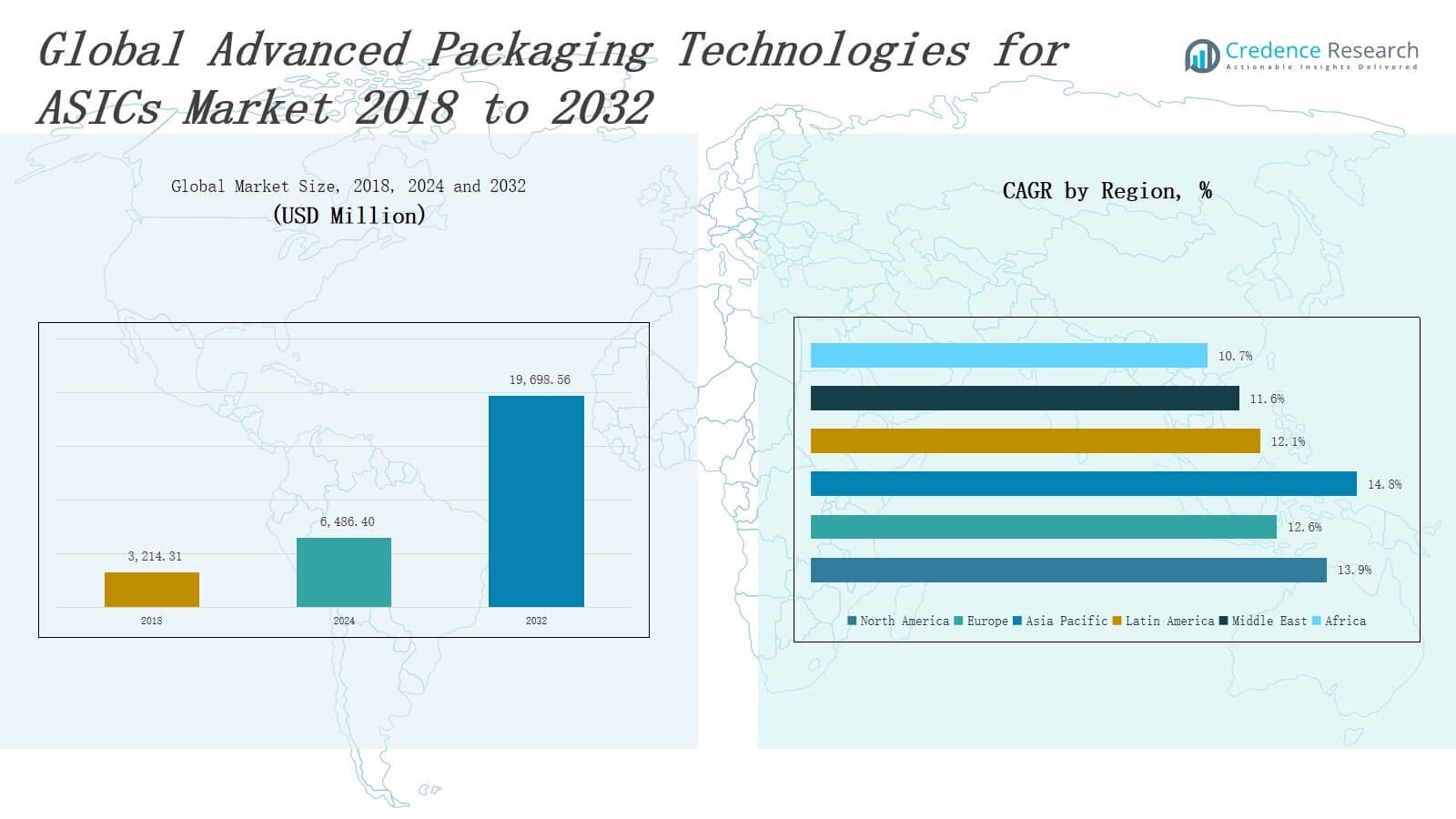
The Advanced Packaging Technologies for ASICs Market size was valued at USD 3,214.31 million in 2018 to USD 6,486.40 million in 2024 and is anticipated to reach USD 19,698.56 million by 2032, at a CAGR of 13.88% during the forecast period.
The Advanced Packaging Technologies for ASICs Market is driven by the growing demand for high-performance, energy-efficient, and miniaturized semiconductor devices across applications such as data centers, consumer electronics, automotive, and telecommunications. The shift toward heterogeneous integration and system-in-package (SiP) designs is accelerating adoption, as advanced packaging enables higher input/output density, reduced power consumption, and improved thermal performance. Market players are prioritizing technologies such as 2.5D/3D integration, fan-out wafer-level packaging (FOWLP), and chiplet architectures to meet rising bandwidth and processing requirements. Trends include increasing deployment of AI and HPC workloads, which require packaging solutions that support higher interconnect speeds and low-latency communication. The transition to advanced nodes like 5nm and 3nm is intensifying the need for sophisticated packaging that ensures signal integrity and electrical performance. Strategic collaborations between foundries, OSATs, and fabless companies are expanding innovation, while sustainability concerns are driving research into eco-friendly materials and energy-efficient manufacturing processes in packaging design.
The Advanced Packaging Technologies for ASICs Market spans six key regions: North America, Europe, Asia Pacific, Latin America, the Middle East, and Africa. Asia Pacific holds the largest share, driven by strong semiconductor manufacturing in China, Taiwan, South Korea, and Japan. North America follows, led by high demand in data centers and automotive sectors. Europe focuses on automotive and industrial applications, while Latin America, the Middle East, and Africa represent emerging markets with growing demand for telecom, consumer electronics, and IoT infrastructure. Leading players in the market include TSMC, Samsung Electronics, Intel Corporation, ASE Technology Holding, Amkor Technology, JCET Group, Advanced Micro Devices (AMD), Siliconware Precision Industries, Powertech Technology Inc., UTAC Holdings Ltd., and Hitachi Ltd. These companies compete through advanced packaging innovations such as 2.5D/3D ICs, chiplets, fan-out packaging, and system-in-package solutions to serve diverse regional and application-specific needs.
Access crucial information at unmatched prices!
Request your sample report today & start making informed decisions powered by Credence Research Inc.!
Download Sample
Market Insights
- The Advanced Packaging Technologies for ASICs Market was valued at USD 6,486.40 million in 2024 and is projected to reach USD 19,698.56 million by 2032, growing at a CAGR of 13.88%.
- Demand for high-performance, low-power ASICs in data centers, automotive systems, and consumer electronics is driving adoption of advanced packaging solutions.
- Technologies such as 2.5D/3D integration, fan-out wafer-level packaging, and chiplets are enabling improved bandwidth, thermal efficiency, and system integration.
- Asia Pacific dominates with a 46% market share, led by Taiwan, China, Japan, and South Korea, while North America holds 29% share driven by strong R&D and data center demand.
- Key players include TSMC, Intel, Samsung, ASE Technology, Amkor, JCET Group, AMD, UTAC Holdings, Hitachi Ltd., Powertech Technology, and Siliconware Precision Industries.
- High production costs, complex workflows, and supply chain constraints limit adoption, especially in cost-sensitive sectors and regions lacking standardization.
- Europe (17% share), Latin America (4%), Middle East (2%), and Africa (1%) show growing interest, especially in automotive, telecom, and smart infrastructure applications.
Market Drivers
Demand for High-Performance and Energy-Efficient Semiconductor Devices
The Advanced Packaging Technologies for ASICs Market is driven by the increasing demand for high-performance, low-power semiconductor devices in data centers, automotive electronics, and consumer products. With rapid AI adoption and edge computing proliferation, chip designers require packaging solutions that support faster data transfer, thermal efficiency, and compact form factors. It enables integration of multiple functionalities in smaller footprints. Energy efficiency and bandwidth optimization remain key priorities across multiple verticals fueling the market’s expansion.
- For instance, TSMC’s CoWoS (Chip-on-Wafer-on-Substrate) technology allows integration of multiple chips within a single package, which is essential for high-performance computing and AI applications due to its ability to boost data transfer rates and reduce power consumption.
Rising Adoption of Heterogeneous Integration and Chiplet Architectures
The shift toward heterogeneous integration and chiplet-based designs is propelling the Advanced Packaging Technologies for ASICs Market forward. It supports performance scaling by allowing multiple dies to function as a single unit, reducing complexity in monolithic SoC development. Demand for flexibility in IP integration and faster time-to-market makes chiplet-based packaging an attractive solution. The technology also improves yield and cost-efficiency by using known-good-die assembly. Major chipmakers are increasing investments in advanced interconnect and substrate innovations.
- For instance, Intel’s Foveros technology enables 3D stacking of logic and memory dies, as seen in its Lakefield processors, allowing for greater flexibility in IP integration and compact form factors.
Growth in AI, 5G, and High-Performance Computing Applications
Rapid deployment of AI, 5G infrastructure, and high-performance computing workloads has created a need for packaging that supports higher input/output density, signal integrity, and thermal reliability. The Advanced Packaging Technologies for ASICs Market benefits from this demand by offering solutions such as 2.5D/3D integration and fan-out wafer-level packaging. These technologies meet rising data throughput and latency requirements. It plays a critical role in enabling multi-functional, multi-core chip designs needed for modern computing environments.
Miniaturization Trends and Need for System-Level Integration
Ongoing trends toward miniaturization and multi-functionality in electronic systems are pushing the boundaries of traditional semiconductor packaging. The Advanced Packaging Technologies for ASICs Market supports this transformation by enabling system-in-package (SiP) designs, which consolidate multiple components into a single module. It improves electrical performance while reducing device size and complexity. OEMs demand such solutions to support wearable electronics, automotive ADAS systems, and IoT applications. This need for integration is fueling innovation in substrate and interposer technologies.
Market Trends
Emergence of 2.5D and 3D Packaging for High-Bandwidth Applications
The Advanced Packaging Technologies for ASICs Market is witnessing strong momentum from the adoption of 2.5D and 3D packaging to meet growing bandwidth and computing performance demands. These architectures enable higher die stacking and shorter interconnect paths, improving data transfer rates and reducing power loss. It supports compact and efficient chip integration for AI, HPC, and networking applications. Companies are developing advanced interposers and through-silicon vias (TSVs) to improve electrical performance and reduce parasitic interference in dense configurations.
- For instance, Fraunhofer IZM has developed customer-specific processes for post-back-end-of-line (BEOL) integration of through-silicon vias (TSVs) into active CMOS wafers, supporting 3DIC-based packaging for applications requiring compact, high-performance system integration.
Rising Popularity of Fan-Out Wafer-Level Packaging (FOWLP)
Fan-out wafer-level packaging continues to gain traction in the Advanced Packaging Technologies for ASICs Market due to its superior electrical performance, thermal efficiency, and ability to support ultra-thin form factors. It eliminates the need for traditional substrates, allowing a higher number of I/Os within a smaller footprint. It is widely adopted in mobile devices and wearable electronics requiring space-saving designs without compromising on speed or power. FOWLP enhances signal integrity while lowering production costs and assembly complexity.
- For instance, TSMC’s InFO (Integrated Fan-Out) technology was used in Apple’s A10 Fusion chip for the iPhone 7, enabling a thinner package and improved power efficiency.
Adoption of Chiplet-Based Design for Flexible Integration
Chiplet architecture is shaping the next wave of innovation in the Advanced Packaging Technologies for ASICs Market. It enables semiconductor manufacturers to build complex systems by assembling multiple specialized dies into a unified package. This trend supports faster design cycles, cost efficiency, and IP reuse across applications. It also enables customization of features like memory, logic, and I/O based on specific workloads. The industry increasingly views chiplets as a viable path forward in overcoming scaling limitations at advanced nodes.
Integration of Advanced Substrates and High-Density Interconnects
Demand for high-density interconnects and advanced substrates is growing in the Advanced Packaging Technologies for ASICs Market due to the need for finer pitch, lower signal delay, and improved power delivery. Substrate innovations such as organic interposers and glass-based materials are enhancing package miniaturization while improving mechanical stability. It enables precise routing for multi-die systems and supports higher frequencies required in HPC and networking. Advanced materials and substrate architectures are critical to achieving next-generation ASIC performance targets.
Market Challenges Analysis
High Cost and Complexity of Manufacturing Processes
The Advanced Packaging Technologies for ASICs Market faces significant challenges related to high production costs and complex manufacturing workflows. Advanced techniques such as 3D integration, chiplet design, and FOWLP require precise process control, expensive materials, and specialized equipment. It increases capital investment requirements for foundries and OSAT providers. Yield management becomes difficult due to tight tolerances and multilayer interconnects. Smaller design houses struggle to adopt these technologies without external support. These factors limit widespread deployment across cost-sensitive sectors.
Supply Chain Constraints and Limited Standardization
The Advanced Packaging Technologies for ASICs Market also contends with supply chain bottlenecks and a lack of industry-wide packaging standards. Delays in the availability of advanced substrates, interposers, and bonding materials disrupt production timelines. It affects time-to-market and scalability, especially for high-volume applications. The absence of standardized design rules and interface protocols for chiplets complicates integration efforts across vendors. Companies must invest in custom solutions, which increases development time and interoperability risks. This slows broader adoption across the ecosystem.
Market Opportunities
Expansion of Edge AI and IoT Applications
The growing demand for edge AI and IoT solutions presents strong opportunities for the Advanced Packaging Technologies for ASICs Market. These applications require compact, power-efficient chips capable of processing data locally with minimal latency. It supports system-in-package (SiP) and fan-out packaging solutions that enable multifunction integration within limited space. The market can benefit from rising deployment in wearables, smart home devices, industrial sensors, and autonomous systems. Emerging economies investing in smart infrastructure further expand the scope for adoption.
Increased Investment in Chiplet Ecosystems and Collaborative Design
Ongoing investment in chiplet ecosystems opens new growth avenues for the Advanced Packaging Technologies for ASICs Market. Industry alliances and open standards initiatives such as UCIe aim to standardize die-to-die interconnects and accelerate chiplet adoption. It allows designers to mix and match dies from different vendors, enhancing flexibility and innovation. The market can leverage these developments to support next-generation computing platforms in data centers, automotive, and aerospace. Collaborative design models reduce risk, improve time-to-market, and foster a broader customer base.
Market Segmentation Analysis:
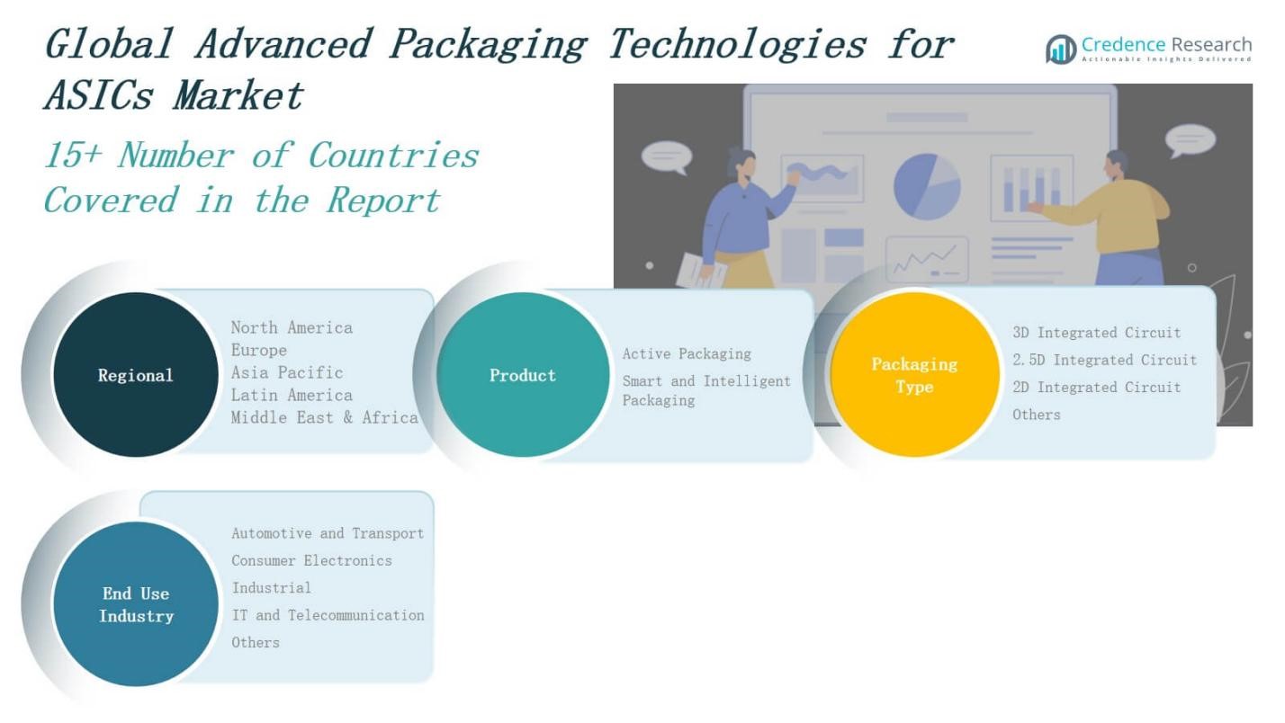
By Product Segment
The Advanced Packaging Technologies for ASICs Market includes active packaging and smart and intelligent packaging. Active packaging supports real-time thermal and power management, making it essential for high-performance applications. Smart and intelligent packaging integrates sensing, monitoring, and adaptive control features that improve system reliability and performance. It addresses the growing need for advanced diagnostics and system optimization in mission-critical environments such as automotive and industrial sectors. Demand for these solutions is increasing with the rise of complex ASIC designs.
- For instance, Nvidia transitioned its Blackwell AI chips from TSMC’s CoWoS-S to the more advanced CoWoS-L packaging, which uses a local silicon interconnect and RDL interposer to improve design flexibility and mitigate yield issues, directly supporting high-performance and reliability requirements for AI workloads.
By Packaging Type
The Advanced Packaging Technologies for ASICs Market is segmented into 3D integrated circuit, 2.5D integrated circuit, 2D integrated circuit, and others. 3D ICs offer superior space efficiency and data throughput by vertically stacking dies, while 2.5D ICs use interposers for high-bandwidth communication between components. 2D ICs remain relevant for less complex applications due to cost efficiency. It supports a range of use cases from mobile devices to servers, depending on performance and integration needs.
- For instance, Samsung’s 3D IC technology is used in its High Bandwidth Memory (HBM2), where multiple DRAM dies are stacked using Through-Silicon Vias (TSVs), enabling data transfer rates up to 307 GB/s per stack in commercial products.
By End Use Industry
The Advanced Packaging Technologies for ASICs Market serves diverse industries including automotive and transport, consumer electronics, industrial, IT and telecommunication, and others. Automotive applications demand high-reliability packaging for ADAS and EV systems. Consumer electronics benefit from compact, energy-efficient solutions for smartphones and wearables. Industrial automation and IoT drive adoption in factory settings. IT and telecom sectors utilize advanced packaging to meet the needs of high-speed data and cloud computing. It enables tailored solutions across varied performance environments.
Segments:
Based on Product
- Active Packaging
- Smart and Intelligent Packaging
Based on Packaging Type
- 3D Integrated Circuit
- 5D Integrated Circuit
- 2D Integrated Circuit
- Other
Based on End Use Industry
- Automotive and Transport
- Consumer Electronics
- Industrial
- IT and Telecommunication
- Others
Based on Region
North America
Europe
- UK, France, Germany, Italy, Spain, Russia, Rest of Europe
Asia Pacific
- China, Japan, South Korea, India, Australia, Southeast Asia, Rest of Asia Pacific
Latin America
- Brazil, Argentina, Rest of Latin America
Middle East
- GCC Countries, Israel, Turkey, Rest of Middle East
Africa
- South Africa, Egypt, Rest of Africa
Regional Analysis
North America
The North America Advanced Packaging Technologies for ASICs Market size was valued at USD 945.75 million in 2018 to USD 1,879.08 million in 2024 and is anticipated to reach USD 5,730.21 million by 2032, at a CAGR of 13.9% during the forecast period. North America holds a 29% market share and leads due to its strong presence of semiconductor manufacturers, advanced R&D infrastructure, and high demand from data centers and automotive sectors. It benefits from widespread adoption of 3D and 2.5D ICs in AI and high-performance computing. Companies such as Intel and AMD continue to drive packaging innovations. Government funding and strong university-industry collaborations also support the region’s dominance.
Europe
The Europe Advanced Packaging Technologies for ASICs Market size was valued at USD 627.53 million in 2018 to USD 1,200.00 million in 2024 and is anticipated to reach USD 3,329.11 million by 2032, at a CAGR of 12.6% during the forecast period. Europe accounts for a 17% market share and focuses on automotive, industrial automation, and telecom applications. The region’s strong automotive supply chain demands robust packaging for sensor fusion, ADAS, and infotainment systems. It leverages advanced packaging for industrial IoT and embedded AI deployments. Germany, France, and the UK serve as key innovation hubs with emphasis on sustainability and system integration.
Asia Pacific
The Asia Pacific Advanced Packaging Technologies for ASICs Market size was valued at USD 1,344.68 million in 2018 to USD 2,818.18 million in 2024 and is anticipated to reach USD 9,103.00 million by 2032, at a CAGR of 14.8% during the forecast period. Asia Pacific dominates with a 46% market share driven by high-volume manufacturing in China, Taiwan, South Korea, and Japan. It benefits from strong consumer electronics and foundry ecosystems. Companies such as TSMC and Samsung lead innovation in fan-out and chiplet packaging. Rapid growth in 5G, AI, and EV sectors fuels continuous demand. Governments across the region invest in semiconductor self-sufficiency and advanced node development.
Latin America
The Latin America Advanced Packaging Technologies for ASICs Market size was valued at USD 151.81 million in 2018 to USD 302.54 million in 2024 and is anticipated to reach USD 813.21 million by 2032, at a CAGR of 12.1% during the forecast period. Latin America holds a 4% market share and shows gradual adoption in industrial automation and consumer electronics. Brazil leads in regional semiconductor demand, supported by manufacturing policies and smart infrastructure development. It remains dependent on imports for advanced packaging solutions but seeks regional partnerships to boost capabilities. The market sees steady traction in telecom and automotive applications.
Middle East
The Middle East Advanced Packaging Technologies for ASICs Market size was valued at USD 93.61 million in 2018 to USD 173.29 million in 2024 and is anticipated to reach USD 447.48 million by 2032, at a CAGR of 11.6% during the forecast period. The region represents a 2% share, driven by digital transformation across smart cities and energy sectors. Countries like the UAE and Saudi Arabia are investing in edge AI and IoT infrastructure. It creates demand for low-power, compact ASIC packaging. The market remains in its early stage, with growth supported by partnerships with global OSAT providers and technology vendors.
Africa
The Africa Advanced Packaging Technologies for ASICs Market size was valued at USD 50.94 million in 2018 to USD 113.30 million in 2024 and is anticipated to reach USD 275.54 million by 2032, at a CAGR of 10.7% during the forecast period. Africa holds a 1% market share, with opportunities emerging from mobile technology and government-led digital initiatives. South Africa leads regional adoption, focusing on telecom and public infrastructure. It faces challenges in supply chain access and technical expertise but seeks long-term capacity building. Local universities and research institutions play a key role in early-stage development.
Shape Your Report to Specific Countries or Regions & Enjoy 30% Off!
Key Player Analysis
- Hitachi Ltd.
- TSMC (Taiwan Semiconductor Manufacturing Company)
- UTAC Holdings Ltd.
- Amkor Technology
- Advanced Micro Devices (AMD)
- JCET Group
- ASE Technology Holding
- Powertech Technology Inc.
- Samsung Electronics
- Intel Corporation
- Siliconware Precision Industries
Competitive Analysis
The Advanced Packaging Technologies for ASICs Market features strong competition among global semiconductor foundries, outsourced semiconductor assembly and test (OSAT) providers, and integrated device manufacturers. Companies such as TSMC, Samsung Electronics, and Intel lead in R&D and scale, offering advanced 2.5D/3D ICs and chiplet-based solutions. Amkor Technology, ASE Technology Holding, and JCET Group focus on high-volume manufacturing and diversified packaging portfolios. It sees increasing investment in fan-out wafer-level packaging, system-in-package (SiP), and heterogeneous integration. Players compete on factors including thermal performance, I/O density, customization, and cost efficiency. Partnerships between fabless firms and packaging specialists are shaping innovation cycles. Startups and regional firms aim to capture niche segments by offering flexible, low-cost solutions tailored to consumer electronics and automotive applications. Market consolidation continues through strategic alliances and acquisitions to expand geographic presence and capabilities. Competitive intensity remains high, driven by rapid technology evolution and the growing need for integration and miniaturization.
Recent Developments
- In June 2025, Astera Labs partnered with Alchip Technologies to co-develop advanced ASIC solutions for AI rack-scale connectivity, combining high-speed interconnects with custom packaging expertise.
- In January 2025, Alchip Technologies launched its new 3DIC ASIC design service, aimed at high-performance computing and AI applications, supporting advanced nodes down to 3nm.
- In May 2025, GlobalFoundries signed an MOU with A*STAR in Singapore to enhance advanced packaging innovation and workforce development.
Market Concentration & Characteristics
The Advanced Packaging Technologies for ASICs Market is moderately concentrated, with a few global players dominating high-end manufacturing and innovation. Companies such as TSMC, Intel, Samsung, ASE Technology, and Amkor Technology hold significant market share due to their advanced R&D capabilities, strong customer relationships, and large-scale production infrastructure. It exhibits high entry barriers driven by capital-intensive processes, specialized equipment, and deep technical expertise required for 2.5D/3D ICs, fan-out packaging, and chiplet-based designs. The market is characterized by rapid technology evolution, demand for system-level integration, and short innovation cycles. Strategic partnerships between foundries, OSATs, and fabless companies are common to accelerate time-to-market and manage design complexity. Regional players compete in niche segments such as consumer electronics and automotive, where customization and cost-efficiency are critical. The market favors companies that offer scalable, low-power, and compact packaging solutions with strong thermal and electrical performance to meet application-specific requirements across data centers, telecom, automotive, and industrial sectors.
Report Coverage
The research report offers an in-depth analysis based on Product, Packaging Type, End-Use Industry and Region. It details leading market players, providing an overview of their business, product offerings, investments, revenue streams, and key applications. Additionally, the report includes insights into the competitive environment, SWOT analysis, current market trends, as well as the primary drivers and constraints. Furthermore, it discusses various factors that have driven market expansion in recent years. The report also explores market dynamics, regulatory scenarios, and technological advancements that are shaping the industry. It assesses the impact of external factors and global economic changes on market growth. Lastly, it provides strategic recommendations for new entrants and established companies to navigate the complexities of the market.
Future Outlook
- Demand for compact, high-performance ASIC packaging will rise due to growing adoption in edge computing and AI applications.
- Chiplet-based architectures will gain wider acceptance, enabling flexible, modular system designs across industries.
- Investments in 2.5D and 3D packaging technologies will increase to support high-bandwidth, multi-die integration.
- Foundries and OSATs will form more strategic alliances to streamline design, testing, and packaging processes.
- The shift toward advanced node semiconductors will require packaging solutions with improved thermal and electrical performance.
- Sustainability goals will drive innovation in eco-friendly packaging materials and energy-efficient manufacturing techniques.
- Fan-out wafer-level packaging will expand in mobile and consumer electronics due to its size and performance benefits.
- Automotive applications will demand rugged, high-reliability packaging for ADAS, battery systems, and autonomous platforms.
- Standardization of chiplet interfaces will accelerate interoperability and reduce design complexity across vendors.
- Regional governments will boost domestic semiconductor capabilities, increasing local demand for advanced packaging solutions.


