Home » Automation & Process Control » GaN-on-SiC Substrates Market

GaN-on-SiC Substrates Market Based on Wafer Size (2-inch (50 mm), 3-inch (75 mm), 4-inch (100 mm), 6-inch (150 mm), 8-inch (200 mm)); Based on Technology (Metal-Organic Chemical Vapor Deposition (MOCVD), Molecular Beam Epitaxy (MBE), Hybrid Vapor Phase Epitaxy (HVPE)); Based on Application (RF Devices: 5G Base Stations, Radars, Satellite Communication; Power Devices: EV Power Modules, Inverters; Optoelectronics: LEDs, Laser Diodes); Based on End-Use Industry (Telecommunications, Automotive, Aerospace & Defense, Consumer Electronics, Others) – Growth, Share, Opportunities & Competitive Analysis, 2024 – 2032

Price: $4699

Published: | Report ID: 111973 | Report Format : Excel, PDF

Market Overview

The GaN-on-SiC Substrates Market size was valued at USD 271.11 million in 2018 to USD 539.00 million in 2024 and is anticipated to reach USD 1,571.32 million by 2032, at a CAGR of 13.34% during the forecast period.

REPORT ATTRIBUTE DETAILS
Historical Period 2020-2023
Base Year 2024
Forecast Period 2025-2032
GaN-on-SiC Substrates Market Size 2024 USD 539.00 million
GaN-on-SiC Substrates Market, CAGR 13.34%
GaN-on-SiC Substrates Market Size 2032 USD 1,571.32 million


The GaN-on-SiC substrates market is driven by rising demand for high-frequency, high-power electronic devices across aerospace, defense, and 5G infrastructure. Superior thermal conductivity and power efficiency of GaN-on-SiC over traditional materials fuel its adoption in RF amplifiers, satellite communication, and radar systems. Market growth is supported by increasing investments in compound semiconductor R&D and expanding deployment of electric vehicles and wireless base stations. Key trends include the shift toward miniaturized, energy-efficient components, integration of GaN technology in LIDAR and power electronics, and growing collaborations between foundries and substrate manufacturers to optimize cost, yield, and production scalability.

The GaN-on-SiC Substrates Market shows strong growth across Asia Pacific, North America, and Europe, with Asia Pacific holding the largest share due to robust semiconductor manufacturing and 5G rollout. North America leads in defense and aerospace adoption, while Europe focuses on automotive and energy-efficient electronics. Latin America, the Middle East, and Africa show emerging demand in telecom and power sectors. Key players include Wolfspeed, Sumitomo Electric Industries, Coherent Corp., Qorvo, MACOM, NGK Insulators, Saint-Gobain, NTT Advanced Technology, Sino Nitride Semiconductor, and Freiberger Compound Materials.

GaN-on-SiC Substrates Market size

Market Insights

  • The GaN-on-SiC Substrates Market was valued at USD 539.00 million in 2024 and is projected to reach USD 1,571.32 million by 2032, growing at a CAGR of 13.34%.
  • Asia Pacific leads the market with a 46% share, driven by robust 5G deployment, EV expansion, and semiconductor manufacturing in China, Japan, and South Korea.
  • North America holds 26% market share, supported by high defense spending, aerospace innovation, and presence of key players like Wolfspeed and Qorvo.
  • Europe contributes 16% of the global market, focusing on automotive electrification, power-efficient electronics, and defense applications.
  • Key growth drivers include demand for high-frequency, high-power devices, superior thermal performance, and expanding 5G and radar infrastructure.
  • Major challenges include high production costs, limited economies of scale, and supply chain constraints related to silicon carbide material sourcing.
  • Prominent players include Wolfspeed, Sumitomo Electric Industries, Coherent Corp., Qorvo, MACOM, NGK Insulators, Saint-Gobain, NTT Advanced Technology, Sino Nitride Semiconductor, and Freiberger Compound Materials.

Design Element 2

Access crucial information at unmatched prices!

Request your sample report today & start making informed decisions powered by Credence Research!

Download Sample

CTA Design Element 3

Market Drivers

Rising Demand for High-Power, High-Frequency Applications

The GaN-on-SiC Substrates Market is propelled by its superior performance in high-power, high-frequency applications. It enables compact, energy-efficient devices ideal for RF amplifiers, radar systems, and satellite communications. Defense and aerospace sectors rely on its thermal conductivity and power density to support mission-critical systems. Telecom operators also benefit from its efficiency in 5G base stations. GaN-on-SiC reduces cooling requirements and extends device lifespan. This demand sustains its growing relevance across critical infrastructure deployments.

  • For instance, in the telecom sector, Nokia has deployed GaN-on-SiC-powered radio units in its AirScale 5G base stations, improving power efficiency and network coverage.

Superiority in Thermal Conductivity and Power Density

Thermal management challenges in modern electronics increase the appeal of GaN-on-SiC substrates. It delivers enhanced heat dissipation and supports higher current densities, outperforming silicon and GaN-on-silicon alternatives. Engineers prioritize it for robust, compact power systems where heat reliability is a concern. The market gains traction in power electronics, especially in harsh environments. Its benefits extend device reliability in defense-grade and aerospace equipment. GaN-on-SiC Substrates Market growth reflects a clear shift in thermal management standards.

  • For instance, GaN devices grown on 4H-SiC substrates demonstrate thermal conductivities comparable to high-quality bulk GaN, ensuring greater heat removal efficiency critical for high-power applications.

Rapid Expansion of 5G and Wireless Infrastructure

Deployment of 5G networks and wireless backhaul drives strong adoption of GaN-on-SiC substrates. Telecom infrastructure providers seek substrates that support high-frequency and wide-band performance. GaN-on-SiC meets this need while improving energy efficiency and reducing signal distortion. It supports the increased data demand and low-latency requirements of modern networks. Countries investing in 5G expansion further amplify this demand. The GaN-on-SiC Substrates Market benefits directly from telecom modernization and spectrum upgrades.

Growing Investments in Advanced Defense and Radar Systems

Defense modernization programs globally incorporate advanced radar and electronic warfare systems requiring GaN-on-SiC. It offers the durability and performance necessary for long-range, high-resolution radar. Governments allocate significant funding toward semiconductor advancements for military applications. GaN-on-SiC ensures stable performance under extreme temperatures and electromagnetic interference. Suppliers expand fabrication capabilities to meet stringent defense standards. The GaN-on-SiC Substrates Market capitalizes on sustained military procurement and technological superiority requirements.

 Market Trends

Increasing Integration in 5G, Aerospace, and Defense Systems

The GaN-on-SiC Substrates Market is witnessing strong traction from its integration in 5G infrastructure, satellite systems, and advanced radar platforms. It supports high-performance RF components that deliver stable operation in wide bandwidth and extreme temperature conditions. OEMs increasingly prefer it for long-range radar, electronic warfare, and base station amplifiers. It enables higher data transmission speeds, lower latency, and improved signal integrity. This trend strengthens its position in high-reliability sectors demanding superior thermal and power performance.

  •  For instance, Raytheon Technologies uses GaN-on-SiC technology in its AN/SPY-6 radar systems to enhance detection range and target resolution for naval defense.

Emergence of Strategic Collaborations and Technology Licensing Deals

Manufacturers and foundries are entering strategic partnerships to improve GaN-on-SiC yield and reduce production costs. This trend involves long-term supply agreements, IP licensing, and joint R&D for scaling substrate innovation. It helps streamline production, improve design customization, and accelerate product qualification. Foundries collaborate with defense contractors and telecom OEMs to meet application-specific requirements. The GaN-on-SiC Substrates Market benefits from this collaborative model that boosts commercial scalability and reduces technological entry barriers for new entrants.

  • For instance, SweGaN in Sweden is expanding its production capacity with a new wafer plant capable of manufacturing up to 40,000 GaN-on-SiC epitaxial wafers annually, supporting applications in 5G, defense, and EV power switches.

Expansion of Wafer Size and Manufacturing Capacity

A key trend involves the transition from 4-inch to 6-inch and even 8-inch GaN-on-SiC wafers to improve throughput and reduce costs. Manufacturers invest in advanced epitaxy and metrology tools to enhance process precision. This enables better substrate uniformity, reduces defects, and improves device yield. It supports large-scale production for RF and power applications. The GaN-on-SiC Substrates Market leverages these manufacturing advancements to meet volume demand from telecom, automotive, and aerospace sectors without compromising on quality.

Growing Adoption in EV Power Modules and High-Voltage Systems

Electric vehicles and renewable energy systems now incorporate GaN-on-SiC substrates for power electronics. It delivers higher breakdown voltage, reduced switching losses, and improved thermal handling over traditional materials. OEMs use it in onboard chargers, inverters, and DC-DC converters. It supports compact designs and higher energy efficiency. The GaN-on-SiC Substrates Market expands its footprint in automotive electrification, driven by performance requirements in high-voltage systems and continuous demand for fast-charging infrastructure.

Market Challenges Analysis

High Manufacturing Costs and Limited Economies of Scale

The GaN-on-SiC Substrates Market faces significant cost-related challenges due to expensive raw materials and complex fabrication processes. Producing high-quality SiC wafers requires advanced crystal growth and polishing techniques, which increase capital expenditure. Small production volumes further limit cost efficiency, hindering broader commercial adoption. It remains a costlier alternative to GaN-on-Silicon in high-volume applications. This cost disparity creates adoption barriers in cost-sensitive sectors such as consumer electronics and industrial automation. Manufacturers must invest in scaling and yield improvement to stay competitive.

Technical Complexity and Supply Chain Constraints

Production of GaN-on-SiC substrates involves intricate epitaxial growth, thermal management, and material compatibility control. Yield rates often fluctuate due to crystal defects and process variability, impacting device reliability and scalability. The GaN-on-SiC Substrates Market struggles with a limited number of qualified suppliers, creating supply bottlenecks and long lead times. It remains vulnerable to geopolitical tensions affecting critical raw materials like silicon carbide. This limits its availability for emerging sectors where consistent supply and design flexibility are essential.

Market Opportunities

Expansion into Power Electronics for Electric Mobility and Renewable Energy

The GaN-on-SiC Substrates Market holds strong potential in electric vehicles and renewable energy systems. Demand for compact, high-efficiency power modules in EV inverters, onboard chargers, and solar inverters creates new growth avenues. It enables faster switching speeds, higher power densities, and improved thermal performance, which are critical for next-generation electrification platforms. Automotive OEMs and energy integrators are testing GaN-on-SiC for advanced traction systems. The market benefits from regulatory mandates promoting low-emission transportation and grid modernization.

Emerging Applications in LIDAR, Satellite Communications, and Space Electronics

Adoption of GaN-on-SiC substrates is expanding into high-frequency, high-reliability applications such as LIDAR, phased-array antennas, and satellite communications. It delivers superior performance under vacuum, radiation, and thermal stress, making it ideal for aerospace missions and deep-space systems. Emerging commercial space ventures seek reliable RF power amplifiers built on GaN-on-SiC. The GaN-on-SiC Substrates Market gains from increasing demand for space-based data services, autonomous vehicle navigation, and advanced defense surveillance systems. It supports a wide range of mission-critical innovations.

Market Segmentation Analysis:

By Wafer Size

The GaN-on-SiC Substrates Market is segmented by wafer size into 2-inch, 3-inch, 4-inch, 6-inch, and 8-inch formats. 4-inch and 6-inch wafers currently dominate the market due to their commercial maturity and higher adoption in RF and power applications. The shift toward 6-inch and 8-inch wafers is accelerating, driven by demand for greater throughput and improved manufacturing economies. It supports large-scale production for telecom and defense sectors. Smaller wafers remain in use for R&D and low-volume specialty applications.

  • For instance, Qorvo continues to utilize 4-inch GaN-on-SiC wafers for its high-frequency defense-grade components, while introducing pilot-scale 6-inch wafer usage for next-gen phased array systems.

By Technology

Based on technology, the GaN-on-SiC Substrates Market includes Metal-Organic Chemical Vapor Deposition (MOCVD), Molecular Beam Epitaxy (MBE), and Hybrid Vapor Phase Epitaxy (HVPE). MOCVD leads the segment due to its proven scalability and consistent film quality. MBE is preferred for precise material control in niche applications, particularly in defense and aerospace. HVPE shows growth potential in high-yield, cost-sensitive production. It helps improve substrate throughput while maintaining quality, making it attractive for telecom and automotive adoption.

  • For instance, Cree (now Wolfspeed) uses MOCVD in its Durham, North Carolina facility for the mass production of GaN-on-SiC substrates used in RF and power electronics. MBE is favored for its atomic-layer precision in defense and aerospace applications.

By Application

The GaN-on-SiC Substrates Market covers RF Devices, Power Devices, and Optoelectronics. RF Devices represent the largest segment, driven by demand from 5G base stations, radar systems, and satellite communication. Power Devices are expanding rapidly with the rise of electric vehicles and renewable energy systems requiring efficient, high-voltage switching components. Optoelectronics holds a smaller share but finds relevance in high-brightness LEDs and advanced laser diodes. It benefits sectors requiring compact, high-performance optical solutions.

GaN-on-SiC Substrates Market segmentation

Segments:

Based on Wafer Size:

  • 2-inch (50 mm)
  • 3-inch (75 mm)
  • 4-inch (100 mm)
  • 6-inch (150 mm)
  • 8-inch (200 mm)

Based on Technology:

  • Metal-Organic Chemical Vapor Deposition (MOCVD)
  • Molecular Beam Epitaxy (MBE)
  • Hybrid Vapor Phase Epitaxy (HVPE)

Based on Application:

  • RF Devices (5G base stations, radars, satellite communication)
  • Power Devices (EV power modules, inverters)
  • Optoelectronics (LEDs, laser diodes)

Based on End-Use Industry:

  • Telecommunications
  • Automotive
  • Aerospace & Defense
  • Consumer Electronics
  • Others

Based on Region:

  • North America
    • U.S.
    • Canada
    • Mexico
  • Europe
    • Germany
    • France
    • U.K.
    • Italy
    • Spain
    • Rest of Europe
  • Asia Pacific
    • China
    • Japan
    • India
    • South Korea
    • South-east Asia
    • Rest of Asia Pacific
  • Latin America
    • Brazil
    • Argentina
    • Rest of Latin America
  • Middle East & Africa
    • GCC Countries
    • South Africa
    • Rest of the Middle East and Africa

Regional Analysis

North America

The North America GaN-on-SiC Substrates Market size was valued at USD 75.49 million in 2018 to USD 147.64 million in 2024 and is anticipated to reach USD 432.29 million by 2032, at a CAGR of 13.4% during the forecast period. North America holds a 26% share of the global market, driven by strong demand from aerospace, defense, and 5G infrastructure. The U.S. leads regional adoption due to high R&D investments and government-backed semiconductor programs. It benefits from robust industrial and military requirements for high-frequency, high-power devices. Defense modernization and satellite communications fuel technology deployment across RF and power segments. Key players in the region include Wolfspeed, Qorvo, and MACOM.

Europe

The Europe GaN-on-SiC Substrates Market size was valued at USD 53.77 million in 2018 to USD 101.40 million in 2024 and is anticipated to reach USD 270.45 million by 2032, at a CAGR of 12.1% during the forecast period. Europe accounts for around 16% of the global market, with growth supported by increased adoption in automotive and industrial power electronics. Germany, France, and the UK lead deployments across EV platforms and defense applications. It benefits from strong collaborations between research institutes and semiconductor manufacturers. The region emphasizes energy-efficient technologies aligned with regulatory targets. European aerospace firms also adopt GaN-on-SiC for radar and communication systems.

Asia Pacific

The Asia Pacific GaN-on-SiC Substrates Market size was valued at USD 119.62 million in 2018 to USD 246.52 million in 2024 and is anticipated to reach USD 762.10 million by 2032, at a CAGR of 14.2% during the forecast period. Asia Pacific dominates the global market with a 46% share, led by China, Japan, South Korea, and Taiwan. It benefits from large-scale semiconductor manufacturing, growing 5G rollout, and expanding EV production. Foundries and OEMs invest in GaN-on-SiC for high-frequency RF devices and power electronics. The region’s government policies and funding boost domestic capabilities. It plays a central role in global supply chains and capacity scaling.

Latin America

The Latin America GaN-on-SiC Substrates Market size was valued at USD 12.26 million in 2018 to USD 24.06 million in 2024 and is anticipated to reach USD 61.73 million by 2032, at a CAGR of 11.5% during the forecast period. Latin America holds a 4% share of the global market, with demand rising from telecom upgrades and renewable energy initiatives. Brazil and Mexico lead regional adoption due to expanding electronics and automotive sectors. It faces challenges related to limited fabrication infrastructure. Government-led clean energy programs are expected to stimulate GaN-based power module integration. Telecom providers explore high-efficiency RF solutions to enhance network capacity.

Middle East

The Middle East GaN-on-SiC Substrates Market size was valued at USD 6.33 million in 2018 to USD 11.29 million in 2024 and is anticipated to reach USD 26.62 million by 2032, at a CAGR of 10.3% during the forecast period. The region accounts for nearly 2% of the global market, driven by defense investments and satellite connectivity initiatives. Countries like Israel and the UAE are deploying GaN-based radar and communication systems. It shows gradual interest in 5G infrastructure and energy-efficient power electronics. Market potential is linked to strategic partnerships with international semiconductor firms. Limited domestic manufacturing capacity presents a challenge for broader uptake.

Africa

The Africa GaN-on-SiC Substrates Market size was valued at USD 3.63 million in 2018 to USD 8.09 million in 2024 and is anticipated to reach USD 18.12 million by 2032, at a CAGR of 9.6% during the forecast period. Africa holds a 1% share of the global market and remains in the early stages of GaN-on-SiC adoption. It sees emerging interest from telecom and off-grid renewable energy sectors. Countries like South Africa and Egypt drive regional demand through modernization projects. It lacks localized semiconductor manufacturing infrastructure. International collaborations may improve access to high-efficiency RF and power technologies. Growth depends on foreign investment and digital connectivity initiatives.

Shape Your Report to Specific Countries or Regions & Enjoy 30% Off!

Key Player Analysis

  • MACOM
  • Sino Nitride Semiconductor
  • Freiberger Compound Materials
  • Qorvo
  • II-VI Incorporated (Coherent Corp.)
  • NGK Insulators
  • Cree, Inc. (Wolfspeed)
  • NTT Advanced Technology
  • Saint-Gobain
  • Sumitomo Electric Industries

Competitive Analysis

The GaN-on-SiC Substrates Market features a competitive landscape led by vertically integrated players and specialized material suppliers. Key companies such as Wolfspeed, Sumitomo Electric Industries, and II-VI Incorporated (Coherent Corp.) focus on expanding wafer production and improving substrate quality. It shows increasing consolidation, with players forming strategic alliances to scale capacity and reduce costs. Firms like MACOM and Qorvo target performance-critical RF applications, while others like NGK Insulators and Saint-Gobain emphasize thermal management solutions. Emerging participants such as Sino Nitride Semiconductor and Freiberger Compound Materials are gaining traction through advanced epitaxy and localized supply models. The market rewards players with strong IP portfolios, high-volume manufacturing capability, and consistent substrate yield. It remains innovation-driven, with technology differentiation in wafer size, thermal conductivity, and defect control influencing competitive positioning. Players invest in facility upgrades and long-term contracts with aerospace, telecom, and automotive customers to secure market share and ensure sustained growth.

Recent Developments

  • In November 2024, MACOM was selected by the U.S. Department of Defense to lead a CHIPS Act-funded project focused on developing advanced GaN-on-SiC technologies for high-voltage RF and microwave systems.
  • In December 2024, ROHM Semiconductor Europe entered a strategic partnership with TSMC to co-develop GaN-based solutions targeting next-generation automotive applications.
  • On April 1, 2025, Sanken Electric, a Japanese semiconductor company, acquired Powdec K.K., a firm specializing in GaN semiconductor epitaxial substrates and GaN crystal growth.
  • On June 30, 2025, Wolfspeed initiated a prepackaged Chapter 11 restructuring to reduce USD 4.6 billion in debt and reinforce its financial position for continued growth in SiC and GaN technologies.

Market Concentration & Characteristics

The GaN-on-SiC Substrates Market exhibits a moderately concentrated structure with a few dominant players controlling a significant share of global production. Key participants such as Wolfspeed, Sumitomo Electric Industries, and Coherent Corp. maintain strong vertical integration and proprietary wafer technologies. It features high entry barriers due to capital-intensive manufacturing, complex crystal growth processes, and strict performance standards. The market prioritizes product quality, substrate uniformity, and yield consistency across applications like RF devices and power modules. It demonstrates strong demand from aerospace, defense, and telecom sectors, requiring substrates with superior thermal management and high-frequency capability. Suppliers focus on expanding wafer sizes and enhancing process control to achieve cost efficiency and scale. Collaborative R&D between foundries and OEMs supports innovation and application-specific customization. The GaN-on-SiC Substrates Market rewards firms with robust technical capabilities, long-term supply contracts, and established relationships with Tier 1 device manufacturers across North America, Asia Pacific, and Europe.

Report Coverage

The research report offers an in-depth analysis based on Wafer Size, Technology, Application, End-User Industry and Region. It details leading market players, providing an overview of their business, product offerings, investments, revenue streams, and key applications. Additionally, the report includes insights into the competitive environment, SWOT analysis, current market trends, as well as the primary drivers and constraints. Furthermore, it discusses various factors that have driven market expansion in recent years. The report also explores market dynamics, regulatory scenarios, and technological advancements that are shaping the industry. It assesses the impact of external factors and global economic changes on market growth. Lastly, it provides strategic recommendations for new entrants and established companies to navigate the complexities of the market.

Future Outlook

  1. Demand for GaN-on-SiC substrates will rise with increasing deployment of 5G infrastructure and mmWave networks.
  2. Adoption in electric vehicle power modules will accelerate due to the need for high-efficiency, compact systems.
  3. Aerospace and defense sectors will expand usage in radar, satellite, and electronic warfare applications.
  4. Manufacturers will focus on scaling 6-inch and 8-inch wafer production to improve yield and reduce costs.
  5. Integration of GaN-on-SiC in LIDAR systems will grow in autonomous driving and industrial automation.
  6. Strategic partnerships between foundries and OEMs will strengthen to address application-specific performance needs.
  7. The supply chain will diversify as new players invest in domestic production and silicon carbide sourcing.
  8. Semiconductor companies will increase R&D spending to improve thermal conductivity and defect density control.
  9. Regulatory push for energy-efficient electronics will support wider adoption across telecom and power sectors.
  10. Emerging markets in Latin America, Middle East, and Africa will create new demand for RF and power solutions.

CHAPTER NO. 1: GENESIS OF THE MARKET         

1.1 Market Prelude – Introduction & Scope

1.2 The Big Picture – Objectives & Vision

1.3 Strategic Edge – Unique Value Proposition

1.4 Stakeholder Compass – Key Beneficiaries

CHAPTER NO. 2: EXECUTIVE LENS

2.1 Pulse of the Industry – Market Snapshot

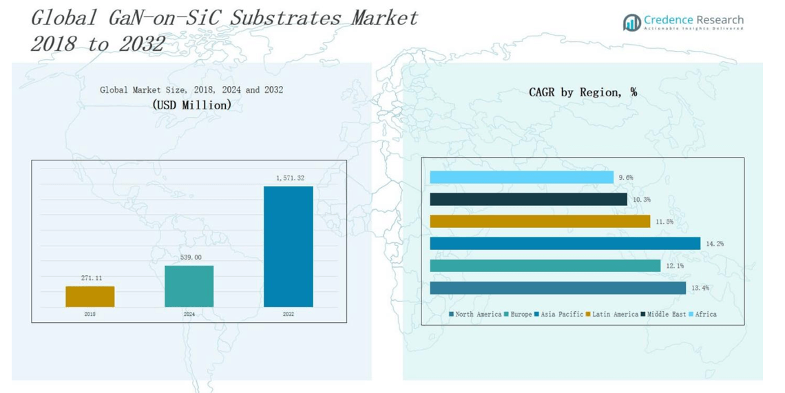
2.2 Growth Arc – Revenue Projections (USD Million)

2.3. Premium Insights – Based on Primary Interviews

CHAPTER NO. 3: GAN-ON-SIC SUBSTRATES MARKET FORCES & INDUSTRY PULSE

3.1 Foundations of Change – Market Overview
3.2 Catalysts of Expansion – Key Market Drivers
3.2.1 Momentum Boosters – Growth Triggers
3.2.2 Innovation Fuel – Disruptive Technologies
3.3 Headwinds & Crosswinds – Market Restraints
3.3.1 Regulatory Tides – Compliance Challenges
3.3.2 Economic Frictions – Inflationary Pressures
3.4 Untapped Horizons – Growth Potential & Opportunities
3.5 Strategic Navigation – Industry Frameworks
3.5.1 Market Equilibrium – Porter’s Five Forces
3.5.2 Ecosystem Dynamics – Value Chain Analysis
3.5.3 Macro Forces – PESTEL Breakdown

3.6 Price Trend Analysis

    3.6.1 Regional Price Trend
3.6.2 Price Trend by Product

CHAPTER NO. 4: KEY INVESTMENT EPICENTER  

4.1 Regional Goldmines – High-Growth Geographies

4.2 Product Frontiers – Lucrative Product Categories

4.3 Application Sweet Spots – Emerging Demand Segments

CHAPTER NO. 5: REVENUE TRAJECTORY & WEALTH MAPPING

5.1 Momentum Metrics – Forecast & Growth Curves

5.2 Regional Revenue Footprint – Market Share Insights

5.3 Segmental Wealth Flow – Wafer Size & Application Revenue

CHAPTER NO. 6: TRADE & COMMERCE ANALYSIS            

6.1.        Import Analysis by Region

6.1.1.     Global GaN-on-SiC Substrates Market Import Revenue By Region

6.2.        Export Analysis by Region

6.2.1.     Global GaN-on-SiC Substrates Market Export Revenue By Region

CHAPTER NO. 7: COMPETITION ANALYSIS           

7.1.        Company Market Share Analysis

7.1.1.     Global GaN-on-SiC Substrates Market: Company Market Share

7.2.        Global GaN-on-SiC Substrates Market Company Revenue Market Share

7.3.        Strategic Developments

7.3.1.     Acquisitions & Mergers

7.3.2.     New Product Launch

7.3.3.     Regional Expansion

7.4.        Competitive Dashboard

7.5.      Company Assessment Metrics, 2024

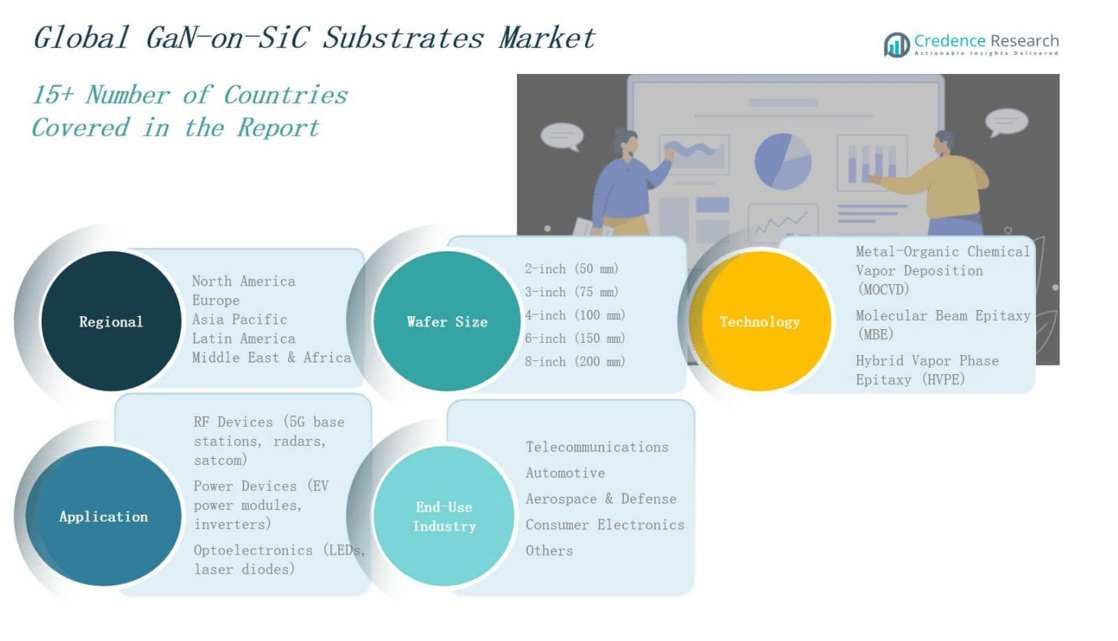
CHAPTER NO. 8: GAN-ON-SIC SUBSTRATES MARKET – BY WAFER SIZE SEGMENT ANALYSIS

8.1.        GaN-on-SiC Substrates Market Overview by Wafer Size Segment

8.1.1.     GaN-on-SiC Substrates Market Revenue Share By Wafer Size

8.2.        2-inch (50 mm)

8.3.        3-inch (75 mm)

8.4.        4-inch (100 mm)

8.5.        6-inch (150 mm)

8.6.        8-inch (200 mm)

CHAPTER NO. 9: GAN-ON-SIC SUBSTRATES MARKET – BY TECHNOLOGY SEGMENT ANALYSIS

9.1.        GaN-on-SiC Substrates Market Overview by Technology Segment

9.1.1.     GaN-on-SiC Substrates Market Revenue Share By Technology

9.2.        Metal-Organic Chemical Vapor Deposition (MOCVD)

9.3.        Molecular Beam Epitaxy (MBE)

9.4.        Hybrid Vapor Phase Epitaxy (HVPE)

CHAPTER NO. 10: GAN-ON-SIC SUBSTRATES MARKET – BY APPLICATION SEGMENT ANALYSIS

10.1.      GaN-on-SiC Substrates Market Overview by Application Segment

10.1.1.  GaN-on-SiC Substrates Market Revenue Share By Application

10.2.      RF Devices (5G base stations, radars, satcom)

10.3.      Power Devices (EV power modules, inverters)

10.4.      Optoelectronics (LEDs, laser diodes)

CHAPTER NO. 11: GAN-ON-SIC SUBSTRATES MARKET – BY END-USE INDUSTRY SEGMENT ANALYSIS

11.1.      GaN-on-SiC Substrates Market Overview by End-Use Industry Segment

11.1.1.  GaN-on-SiC Substrates Market Revenue Share By End-Use Industry

11.2.      Telecommunications

11.3.      Automotive

11.4.      Aerospace & Defense

11.5.      Consumer Electronics

11.6.      Others

CHAPTER NO. 12: GAN-ON-SIC SUBSTRATES MARKET – REGIONAL ANALYSIS

12.1.      GaN-on-SiC Substrates Market Overview by Region Segment

12.1.1.  Global GaN-on-SiC Substrates Market Revenue Share By Region

12.1.2.  Regions

12.1.3.  Global GaN-on-SiC Substrates Market Revenue By Region

12.1.4.  Wafer Size

12.1.5.  Global GaN-on-SiC Substrates Market Revenue By Wafer Size

12.1.6.  Technology

12.1.7.  Global GaN-on-SiC Substrates Market Revenue By Technology

12.1.8.  Application

12.1.9.  Global GaN-on-SiC Substrates Market Revenue By Application

12.1.10. End-Use Industry

12.1.11. Global GaN-on-SiC Substrates Market Revenue By End-Use Industry

CHAPTER NO. 13: NORTH AMERICA GAN-ON-SIC SUBSTRATES MARKET – COUNTRY ANALYSIS

13.1.      North America GaN-on-SiC Substrates Market Overview by Country Segment

13.1.1.  North America GaN-on-SiC Substrates Market Revenue Share By Region

13.2.      North America

13.2.1.  North America GaN-on-SiC Substrates Market Revenue By Country

13.2.2.  Wafer Size

13.2.3.  North America GaN-on-SiC Substrates Market Revenue By Wafer Size

13.2.4.  Technology

13.2.5.  North America GaN-on-SiC Substrates Market Revenue By Technology

13.2.6.  Application

13.2.7.  North America GaN-on-SiC Substrates Market Revenue By Application

13.2.8.  End-Use Industry

13.2.9.  North America GaN-on-SiC Substrates Market Revenue By End-Use Industry

13.3.      U.S.

13.4.      Canada

13.5.      Mexico

CHAPTER NO. 14: EUROPE GAN-ON-SIC SUBSTRATES MARKET – COUNTRY ANALYSIS

14.1.      Europe GaN-on-SiC Substrates Market Overview by Country Segment

14.1.1.  Europe GaN-on-SiC Substrates Market Revenue Share By Region

14.2.      Europe

14.2.1.  Europe GaN-on-SiC Substrates Market Revenue By Country

14.2.2.  Wafer Size

14.2.3.  Europe GaN-on-SiC Substrates Market Revenue By Wafer Size

14.2.4.  Technology

14.2.5.  Europe GaN-on-SiC Substrates Market Revenue By Technology

14.2.6.  Application

14.2.7.  Europe GaN-on-SiC Substrates Market Revenue By Application

14.2.8.  End-Use Industry

14.2.9.  Europe GaN-on-SiC Substrates Market Revenue By End-Use Industry

14.3.      UK

14.4.      France

14.5.      Germany

14.6.      Italy

14.7.      Spain

14.8.      Russia

14.9.   Rest of Europe

CHAPTER NO. 15: ASIA PACIFIC GAN-ON-SIC SUBSTRATES MARKET – COUNTRY ANALYSIS

15.1.      Asia Pacific GaN-on-SiC Substrates Market Overview by Country Segment

15.1.1.  Asia Pacific GaN-on-SiC Substrates Market Revenue Share By Region

15.2.      Asia Pacific

15.2.1.  Asia Pacific GaN-on-SiC Substrates Market Revenue By Country

15.2.2.  Wafer Size

15.2.3.  Asia Pacific GaN-on-SiC Substrates Market Revenue By Wafer Size

15.2.4.  Technology

15.2.5.  Asia Pacific GaN-on-SiC Substrates Market Revenue By Technology

15.2.6.  Application

15.2.7.  Asia Pacific GaN-on-SiC Substrates Market Revenue By Application

15.2.8.  End-Use Industry

15.2.9.  Asia Pacific GaN-on-SiC Substrates Market Revenue By End-Use Industry

15.3.      China

15.4.      Japan

15.5.      South Korea

15.6.      India

15.7.      Australia

15.8.      Southeast Asia

15.9.      Rest of Asia Pacific

CHAPTER NO. 16: LATIN AMERICA GAN-ON-SIC SUBSTRATES MARKET – COUNTRY ANALYSIS

16.1.      Latin America GaN-on-SiC Substrates Market Overview by Country Segment

16.1.1.  Latin America GaN-on-SiC Substrates Market Revenue Share By Region

16.2.      Latin America

16.2.1.  Latin America GaN-on-SiC Substrates Market Revenue By Country

16.2.2.  Wafer Size

16.2.3.  Latin America GaN-on-SiC Substrates Market Revenue By Wafer Size

16.2.4.  Technology

16.2.5.  Latin America GaN-on-SiC Substrates Market Revenue By Technology

16.2.6.  Application

16.2.7.  Latin America GaN-on-SiC Substrates Market Revenue By Application

16.2.8.  End-Use Industry

16.2.9.  Latin America GaN-on-SiC Substrates Market Revenue By End-Use Industry

16.3.      Brazil

16.4.      Argentina

16.5.      Rest of Latin America

CHAPTER NO. 17: MIDDLE EAST GAN-ON-SIC SUBSTRATES MARKET – COUNTRY ANALYSIS

17.1.      Middle East GaN-on-SiC Substrates Market Overview by Country Segment

17.1.1.  Middle East GaN-on-SiC Substrates Market Revenue Share By Region

17.2.      Middle East

17.2.1.  Middle East GaN-on-SiC Substrates Market Revenue By Country

17.2.2.  Wafer Size

17.2.3.  Middle East GaN-on-SiC Substrates Market Revenue By Wafer Size

17.2.4.  Technology

17.2.5.  Middle East GaN-on-SiC Substrates Market Revenue By Technology

17.2.6.  Application

17.2.7.  Middle East GaN-on-SiC Substrates Market Revenue By Application

17.2.8.  End-Use Industry

17.2.9.  Middle East GaN-on-SiC Substrates Market Revenue By End-Use Industry

17.3.      GCC Countries

17.4.      Israel

17.5.      Turkey

17.6.      Rest of Middle East

CHAPTER NO. 18: AFRICA GAN-ON-SIC SUBSTRATES MARKET – COUNTRY ANALYSIS

18.1.      Africa GaN-on-SiC Substrates Market Overview by Country Segment

18.1.1.  Africa GaN-on-SiC Substrates Market Revenue Share By Region

18.2.      Africa

18.2.1.  Africa GaN-on-SiC Substrates Market Revenue By Country

18.2.2.  Wafer Size

18.2.3.  Africa GaN-on-SiC Substrates Market Revenue By Wafer Size

18.2.4.  Technology

18.2.5.  Africa GaN-on-SiC Substrates Market Revenue By Technology

18.2.6.  Application

18.2.7.  Africa GaN-on-SiC Substrates Market Revenue By Application

18.2.8.  End-Use Industry

18.2.9.  Africa GaN-on-SiC Substrates Market Revenue By End-Use Industry

18.3.      South Africa

18.4.      Egypt

18.5.      Rest of Africa

CHAPTER NO. 19: COMPANY PROFILES 

19.1.      Cree, Inc. (Wolfspeed)

19.1.1.  Company Overview

19.1.2.  Product Portfolio

19.1.3.  Financial Overview

19.1.4.  Recent Developments

19.1.5.  Growth Strategy

19.1.6.  SWOT Analysis

19.2.      Sumitomo Electric Industries

19.3.      II-VI Incorporated (Coherent Corp.)

19.4.      Qorvo

19.5.      MACOM

19.6.      NTT Advanced Technology

19.7.      NGK Insulators

19.8.      Saint-Gobain

19.9.      Sino Nitride Semiconductor

19.10.    Freiberger Compound Materials

Frequently Asked Questions

What is the current size of the GaN-on-SiC Substrates Market?

The GaN-on-SiC Substrates Market was valued at USD 539.00 million in 2024 and is projected to reach USD 1,571.32 million by 2032.

What are the key segments within the GaN-on-SiC Substrates Market?

Key segments include wafer size (2–8 inch), technology (MOCVD, MBE, HVPE), application (RF, power, optoelectronics), and end-use industries like telecom and automotive.

What are some challenges faced by the GaN-on-SiC Substrates Market?

Challenges include high manufacturing costs, complex fabrication processes, supply chain constraints, and limited economies of scale in commercial-scale production.

Who are the major players in the GaN-on-SiC Substrates Market?

Major players include Wolfspeed, Sumitomo Electric, Coherent Corp., Qorvo, MACOM, NGK Insulators, Saint-Gobain, NTT Advanced Technology, and Freiberger Compound Materials.

About Author

Sushant Phapale

Sushant Phapale

ICT & Automation Expert

Sushant is an expert in ICT, automation, and electronics with a passion for innovation and market trends.

View Profile

Gunakesh Parmar

Reviewed By
Gunakesh Parmar

Research Consultant

With over 15 years of dedicated experience in market research since 2009, specializes in delivering actionable insights from data.

View Profile

End-of-Line Packaging Market

Published:
Report ID: 112642

Marine Climate Control Systems Market

Published:
Report ID: 112666

Tire Testing Machine Market

Published:
Report ID: 110716

Spent Adsorbent Regeneration Market

Published:
Report ID: 112032

Marine Boiler Burner Market

Published:
Report ID: 111662

Kayak Trolling Motor Market

Published:
Report ID: 111333

Paper Making Machine Market

Published:
Report ID: 111368

Deionized Water Systems Market

Published:
Report ID: 111022

Smart Home and Building Automation ASIC Market

Published:
Report ID: 110641

Shirt Printing Machines Market

Published:
Report ID: 110547

Submersible Pumps Market

Published:
Report ID: 9988

Fermenters Market

Published:
Report ID: 108797

Purchase Options

The report comes as a view-only PDF document, optimized for individual clients. This version is recommended for personal digital use and does not allow printing.
$4699

To meet the needs of modern corporate teams, our report comes in two formats: a printable PDF and a data-rich Excel sheet. This package is optimized for internal analysis and multi-location access, making it an excellent choice for organizations with distributed workforce.
$5699

The report will be delivered in printable PDF format along with the report’s data Excel sheet. This license offers 100 Free Analyst hours where the client can utilize Credence Research Inc.’s research team. It is highly recommended for organizations seeking to execute short, customized research projects related to the scope of the purchased report.
$12699

Credence Staff 3

WILLIAM, North America

Support Staff at Credence Research

KEITH PHILLIPS, Europe

Lee - CR Sales Staff

LEE VALLANCE, Asia Pacific

Kieran Jameson

KIERAN JAMESON, Australia

Smallform of Sample request

Report delivery within 24 to 48 hours

What people say?-

User Review

I am very impressed with the information in this report. The author clearly did their research when they came up with this product and it has already given me a lot of ideas.

Jana Schmidt
CEDAR CX Technologies

– Connect with us –


support

24/7 Research Support


– Research Methodology –

Going beyond the basics: advanced techniques in research methodology

Pepshi, LG, Nestle
Motorola, Honeywell, Johnson and johnson
LG Chem, SIEMENS, Pfizer
Unilever, Samsonite, QIAGEN

Request Sample