Market Overview
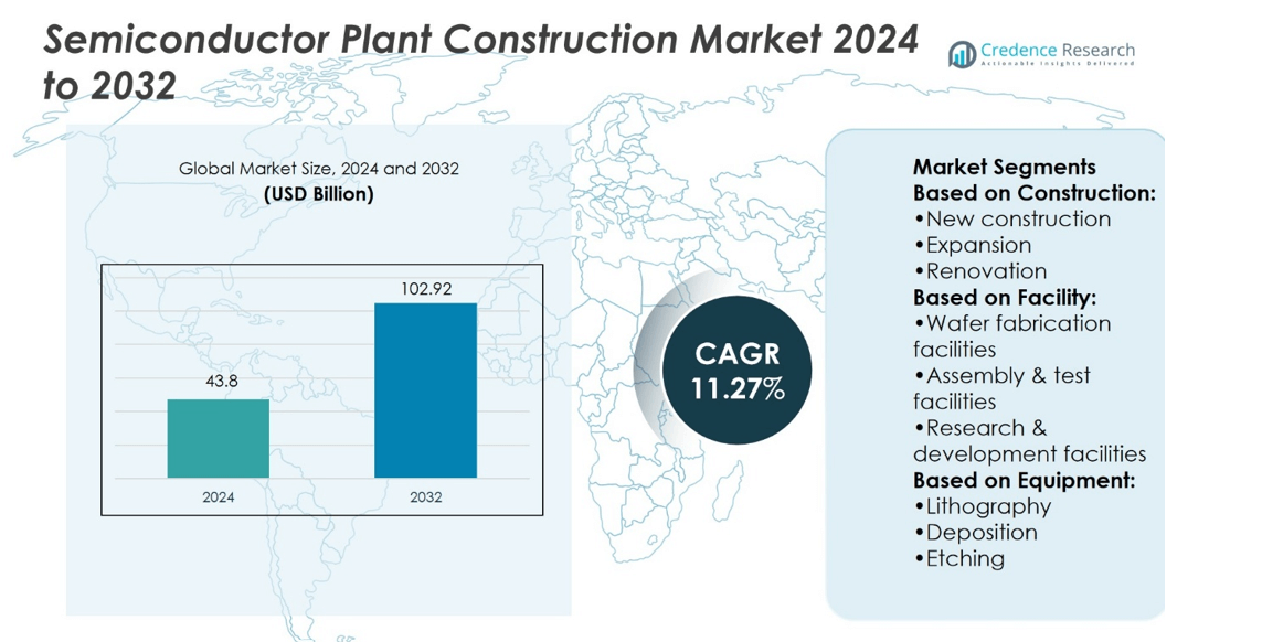
Semiconductor Plant Construction Market size was valued at USD 43.8 billion in 2024 and is anticipated to reach USD 102.92 billion by 2032, at a CAGR of 11.27% during the forecast period.
| REPORT ATTRIBUTE |
DETAILS |
| Historical Period |
2020-2023 |
| Base Year |
2024 |
| Forecast Period |
2025-2032 |
| Semiconductor Plant Construction Market Size 2024 |
USD 43.8 billion |
| Semiconductor Plant Construction Market, CAGR |
11.27% |
| Semiconductor Plant Construction Market Size 2032 |
USD 102.92 billion |
Rising global demand for semiconductors drives investments in new fabrication, assembly, and R&D facilities. The Semiconductor Plant Construction Market focuses on high-capacity, energy-efficient, and automation-ready plants to support next-generation chip production. Companies adopt smart manufacturing, digital integration, and advanced equipment like lithography, deposition, and etching tools to improve yield and operational efficiency. Expansion and renovation of existing facilities enable scalable production and cost optimization. Regional diversification strengthens supply chains and reduces dependency on traditional hubs. Sustainable designs and regulatory compliance remain priorities, while innovation in plant layouts and modular systems supports flexibility, future upgrades, and long-term competitiveness.
North America leads the Semiconductor Plant Construction Market, followed by Asia-Pacific and Europe, supported by advanced infrastructure and government incentives. Latin America and the Middle East & Africa show emerging growth through new and expansion projects. The market includes key players delivering turnkey solutions, cleanroom systems, and automation-ready facilities. Companies focus on high-capacity wafer fabrication, assembly, and R&D plants while integrating energy-efficient designs and smart technologies. Regional diversification strengthens supply chains, supports innovation, and ensures operational reliability across global semiconductor hubs.
Market Insights
- Semiconductor Plant Construction Market size was USD 43.8 billion in 2024, projected USD 102.92 billion by 2032 at 11.27% CAGR.
- Rising demand for semiconductors drives investments in fabrication, assembly, and advanced R&D facilities.
- Market trends emphasize energy-efficient, automation-ready, and smart manufacturing-enabled plant designs.
- Competitive players deliver turnkey solutions, cleanroom systems, and high-capacity wafer fabrication facilities.
- Key restraints include high capital intensity, supply chain risks, and strict regulatory requirements.
- North America leads due to advanced infrastructure and government incentives, followed by Asia-Pacific and Europe.
- Latin America and the Middle East & Africa display emerging growth with new construction and expansion projects.
Access crucial information at unmatched prices!
Request your sample report today & start making informed decisions powered by Credence Research Inc.!
Download Sample
Market Drivers
Rising Demand for Advanced Semiconductor Technologies Driving Construction Projects
The growing adoption of advanced semiconductor technologies fuels the need for new and upgraded fabrication facilities. Companies require highly specialized plants to meet the increasing demand for microchips, logic devices, and memory products. It enables manufacturers to produce high-performance chips with improved efficiency and reduced defects. Semiconductor Plant Construction Market witnesses significant investment in cleanrooms, automation systems, and energy-efficient infrastructure. Governments and private entities prioritize construction projects to support strategic technology initiatives. Firms gain a competitive edge by establishing modern plants with scalable production capacity. It also strengthens regional manufacturing capabilities to meet global supply requirements.
- For instance, Terra Universal designs over 500 cleanrooms annually and builds pre-engineered, quality-control-tested cleanroom components for fast deployment. Its Smart® Fan Filter Units (FFUs) with EC motors feature infinitely variable speed control.
Expansion of Regional Semiconductor Ecosystems Promoting Facility Development
Emerging semiconductor hubs in Asia-Pacific, Europe, and North America drive construction activity. It allows manufacturers to localize production, reduce logistics costs, and comply with regional regulations. Companies benefit from proximity to suppliers, research centers, and skilled workforce. Semiconductor Plant Construction Market experiences growth in regions offering tax incentives, subsidies, and infrastructure support. Collaborative efforts between governments and industry players accelerate plant establishment and operational readiness. It encourages companies to invest in multi-phase construction projects with flexible layouts. This trend fosters competitive regional ecosystems while supporting global semiconductor demand.
- For instance, Horton Automatics equipped TSMC’s Phoenix semiconductor plant with nearly 200 ISO 3-rated sliding doors, ensuring cleanroom integrity and energy efficiency in the 5-nm chip facility.
Investment in Sustainable and Energy-Efficient Semiconductor Facilities
Sustainability requirements and energy efficiency standards shape plant design and construction practices. Semiconductor Plant Construction Market emphasizes eco-friendly materials, renewable energy integration, and waste management systems. It reduces operational costs and aligns with corporate environmental commitments. Companies prioritize modular facility designs to enable upgrades and minimize resource consumption. Investors focus on projects that balance high-performance production with low environmental impact. It enhances corporate reputation and meets increasing regulatory expectations. Advanced monitoring and control systems support efficient energy usage across production processes.
Technological Advancements in Automation and Smart Facility Integration
Automation and smart manufacturing solutions enhance semiconductor production efficiency and reliability. Semiconductor Plant Construction Market incorporates robotics, AI-driven process controls, and advanced monitoring systems. It enables real-time tracking, predictive maintenance, and improved yield management. Companies reduce manual interventions and minimize errors through intelligent plant layouts. Integration of digital twins and IoT networks allows continuous optimization of operations. It supports rapid adaptation to changing product requirements and market trends. Investments in smart facilities ensure long-term competitiveness in a dynamic semiconductor industry.
Market Trends
Shift Towards High-Capacity and Advanced Fabrication Facilities
The demand for high-capacity semiconductor production drives the development of state-of-the-art fabrication plants. Semiconductor Plant Construction Market focuses on expanding wafer production lines and incorporating advanced lithography equipment. It enables manufacturers to meet growing global requirements for memory chips, microprocessors, and specialized ICs. Companies prioritize facilities that support smaller node sizes and higher transistor densities. Investments target flexible layouts that allow future expansions without disrupting operations. It strengthens competitive positioning by improving throughput and reducing defect rates. Firms also integrate automation to enhance production efficiency and maintain consistent quality.
- For instance, SKAN Group offers modular ISO 7 cleanroom kits designed for fast and efficient installation, which can be adapted and expanded as needed. This modular design helps to minimize on-site disruption, reducing potential downtime during facility expansions.
Regional Diversification of Semiconductor Manufacturing Hubs
Emerging regions seek to reduce dependence on traditional manufacturing centers, fueling new plant construction projects. Semiconductor Plant Construction Market witnesses growth in Asia-Pacific, Europe, and North America through strategic investments. It allows companies to access local talent, suppliers, and government incentives. Multi-site manufacturing strategies improve supply chain resilience and minimize logistical risks. Firms adopt modular plant designs to quickly scale production in response to market demand. It enhances regional semiconductor ecosystems while supporting domestic technological initiatives. Investors monitor geopolitical trends to optimize plant location and long-term operational stability.
- For instance, IPS delivered a semiconductor manufacturing expansion in Greensboro, NC. They transformed 18,000 sf of shell space, installed 80 processing tools (set S800), and engineered HVAC systems delivering 700,000 CFM via 22.
Integration of Smart Technologies and Digital Infrastructure in Plants
Smart facility integration drives efficiency, safety, and predictive operations in semiconductor production. Semiconductor Plant Construction Market incorporates IoT sensors, AI monitoring systems, and digital twins. It allows real-time process analysis, predictive maintenance, and reduced operational downtime. Companies improve energy management and process accuracy by integrating advanced control systems. Facilities adopt data-driven decision-making to enhance overall performance. It also facilitates seamless integration of new equipment and technologies. This trend promotes high operational flexibility and ensures future-ready production capabilities.
Focus on Sustainable and Environmentally Compliant Semiconductor Facilities
Environmental regulations and corporate sustainability commitments influence plant construction strategies. Semiconductor Plant Construction Market emphasizes energy-efficient designs, water recycling, and emission control measures. It reduces operating costs and strengthens compliance with global standards. Companies integrate renewable energy sources and low-impact materials in construction. Facility layouts optimize airflow, temperature, and resource consumption to maintain efficiency. It enables long-term sustainability while supporting corporate responsibility initiatives. Investors increasingly prioritize green-certified plants to meet stakeholder expectations and market demands.
Market Challenges Analysis
High Capital Requirements and Financial Constraints Limiting Expansion Opportunities
Semiconductor Plant Construction Market faces significant challenges due to the high capital investment required for facility development. It demands extensive funding for land acquisition, advanced equipment, and specialized cleanroom infrastructure. Companies encounter difficulties in securing financial resources, especially for multi-phase or large-scale projects. Budget constraints can delay project timelines and limit the adoption of cutting-edge technologies. Investors remain cautious due to fluctuating demand cycles and global supply chain uncertainties. It also impacts the ability to maintain competitive production capacity and achieve rapid ROI. Firms must carefully balance cost management with technological advancement to sustain growth.
Complex Regulatory Compliance and Supply Chain Vulnerabilities Affecting Operations
Compliance with stringent environmental, safety, and zoning regulations poses challenges for semiconductor plant development. Semiconductor Plant Construction Market must navigate multiple local, national, and international regulatory frameworks. It requires continuous monitoring and adaptation to maintain operational approvals and certifications. Supply chain disruptions for critical materials and machinery create further obstacles. Companies face delays and increased costs due to limited availability of specialized construction components. It also affects scheduling, production ramp-up, and overall operational efficiency. Firms must implement robust risk management strategies to mitigate regulatory and supply chain challenges while sustaining long-term competitiveness.
Market Opportunities
Expansion of Greenfield and Brownfield Semiconductor Projects Offering Growth Potential
The rising global demand for semiconductors creates opportunities for new greenfield and brownfield construction projects. Semiconductor Plant Construction Market benefits from investments in modern fabrication facilities and upgrades to existing plants. It allows companies to increase production capacity and adopt advanced manufacturing technologies. Governments offer incentives, subsidies, and tax benefits to encourage domestic facility development. Companies can leverage scalable plant designs to meet evolving market requirements efficiently. It supports strategic positioning in emerging regions with growing semiconductor ecosystems. Firms gain competitive advantage through timely project execution and operational readiness.
Adoption of Smart Manufacturing and Digital Integration Enhancing Competitive Edge
Integration of automation, IoT, and AI-driven systems in plant construction opens new avenues for efficiency and innovation. Semiconductor Plant Construction Market experiences opportunities to implement digital twins, predictive maintenance, and advanced process control. It enables real-time monitoring, quality assurance, and energy optimization. Companies can reduce operational costs while maintaining high throughput and consistent product quality. Collaboration with technology providers fosters the development of state-of-the-art smart facilities. It strengthens long-term competitiveness and supports rapid adaptation to market shifts. Firms investing in these innovations position themselves as leaders in advanced semiconductor manufacturing.
Market Segmentation Analysis:
By Construction
New construction projects drive the Semiconductor Plant Construction Market by creating state-of-the-art facilities to meet rising semiconductor demand. It allows companies to implement modern layouts, energy-efficient designs, and automation-ready infrastructure. Expansion projects focus on increasing production capacity within existing plants, supporting scalable operations and faster time-to-market. Renovation of older facilities modernizes cleanrooms, upgrades utilities, and integrates advanced equipment to improve yield and reduce defects. Companies prioritize renovation to extend plant lifespan and maintain competitiveness. It also reduces overall project costs compared to constructing entirely new plants. These three constructions approach collectively ensure the industry adapts to evolving technology and market needs.
- For instance, Exyte has opened a new engineering and project execution hub in Dresden—spanning 2,700 m² over five floors and hosting up to 150 engineering staff, enhancing agility in Silicon Saxony’s semiconductor cluster.
By Facility
Wafer fabrication facilities represent the core segment, hosting critical processes like photolithography, etching, and deposition. Semiconductor Plant Construction Market emphasizes precision, contamination control, and high-capacity production in these plants. Assembly and test facilities focus on packaging, quality control, and reliability verification of semiconductor devices. It enables rapid product validation and ensures compliance with performance standards. Research and development facilities support innovation, prototyping, and advanced material testing. Companies invest in R&D spaces to develop next-generation chips and enhance technological capabilities. It strengthens product differentiation and long-term growth potential.
- For instance, Enviro-Tec offers various indoor air-handling units and fan coil units to enable precise environmental control in critical environments. Some fan coil unit models range from 250 to 2,400 CFM. Its ESL series of indoor air-handlers, designed for larger applications, is available in sizes ranging from 1,000 to 30,000 CFM.
By Equipment
Lithography equipment forms a critical part of semiconductor plant infrastructure, enabling precise patterning for advanced nodes. Semiconductor Plant Construction Market integrates deposition tools for thin-film formation and material layering. It ensures high uniformity, consistency, and efficiency across wafers. Etching tools remove specific material regions to define circuit features accurately. Companies prioritize these equipment segments to maintain production accuracy and reduce defect rates. It supports both high-volume manufacturing and experimental R&D projects. Strategic investment in advanced equipment enhances plant performance, flexibility, and overall competitiveness in the global semiconductor landscape.
Segments:
Based on Construction:
- New construction
- Expansion
- Renovation
Based on Facility:
- Wafer fabrication facilities
- Assembly & test facilities
- Research & development facilities
Based on Equipment:
- Lithography
- Deposition
- Etching
Based on the Geography:
- North America
- Europe
- UK
- France
- Germany
- Italy
- Spain
- Russia
- Belgium
- Netherlands
- Austria
- Sweden
- Poland
- Denmark
- Switzerland
- Rest of Europe
- Asia Pacific
- China
- Japan
- South Korea
- India
- Australia
- Thailand
- Indonesia
- Vietnam
- Malaysia
- Philippines
- Taiwan
- Rest of Asia Pacific
- Latin America
- Brazil
- Argentina
- Peru
- Chile
- Colombia
- Rest of Latin America
- Middle East
- UAE
- KSA
- Israel
- Turkey
- Iran
- Rest of Middle East
- Africa
- Egypt
- Nigeria
- Algeria
- Morocco
- Rest of Africa
Regional Analysis
North America
North America dominates the Semiconductor Plant Construction Market with a 32% share due to the presence of major semiconductor manufacturers and advanced technological infrastructure. The U.S. leads with large-scale wafer fabrication facilities and R&D centers supporting next-generation chip development. It benefits from government incentives, tax credits, and funding programs that promote domestic plant construction and modernization projects. Companies prioritize high-capacity production and smart facility integration to maintain global competitiveness. The region also experiences steady expansion of assembly and test facilities to support end-use sectors like automotive, aerospace, and consumer electronics. It emphasizes sustainable designs, energy-efficient cleanrooms, and advanced lithography equipment. Investments in automation and digital integration further strengthen plant productivity and operational efficiency.
Europe
Europe captures a 21% share of the Semiconductor Plant Construction Market, driven by robust industrial and automotive sectors. Germany, France, and the Netherlands lead with high-capacity wafer fabrication and assembly plants. It focuses on meeting stringent environmental regulations, integrating energy-efficient systems, and adopting sustainable construction practices. Expansion and renovation projects are common to upgrade legacy facilities with advanced lithography, deposition, and etching tools. European companies invest in R&D facilities to support innovation in microelectronics and power semiconductors. It benefits from collaborative efforts between governments, research institutions, and private players. Advanced automation systems and digital monitoring solutions enhance throughput, quality, and reliability.
Asia-Pacific
Asia-Pacific holds a 30% share of the Semiconductor Plant Construction Market, reflecting rapid industrialization and growing semiconductor demand. China, Taiwan, South Korea, and Japan lead in new wafer fabrication and assembly facility projects. It enables local manufacturers to reduce import dependence and improve supply chain efficiency. Expansion projects in the region focus on increasing production capacity for memory, logic, and specialty chips. Companies integrate advanced deposition, etching, and lithography equipment to maintain production precision and yield. It emphasizes large-scale R&D facilities to drive innovation and support domestic technology initiatives. Government incentives, favorable policies, and access to skilled labor attract continued investment. The region also prioritizes energy-efficient and environmentally compliant construction practices.
Latin America
Latin America accounts for a 9% share of the Semiconductor Plant Construction Market, supported by emerging manufacturing hubs in Brazil, Mexico, and Chile. It experiences moderate growth through small- to mid-scale fabrication and assembly facilities targeting regional demand. Expansion projects focus on upgrading legacy plants to meet quality standards and regulatory compliance. Companies adopt modern equipment, including lithography, etching, and deposition tools, to enhance production capabilities. It also promotes regional R&D facilities for prototyping and product testing. Strategic collaborations with global semiconductor players support technology transfer and workforce development. Investments in smart plant systems improve efficiency and reliability.
Middle East & Africa
Middle East & Africa represent an 8% share of the Semiconductor Plant Construction Market, driven by industrial diversification and government-backed initiatives. Countries such as the UAE, Saudi Arabia, and South Africa invest in new fabrication and assembly plants to establish domestic semiconductor capabilities. It focuses on integrating automation, cleanroom infrastructure, and advanced equipment for efficient production. Expansion projects aim to upgrade existing facilities and attract international manufacturers. Companies invest in R&D centers to support innovation and localized product development. It benefits from partnerships with global technology providers and strategic government policies. Sustainable facility design and energy-efficient operations remain priorities for long-term competitiveness.
Shape Your Report to Specific Countries or Regions & Enjoy 30% Off!
Key Player Analysis
Competitive Analysis
The Semiconductor Plant Construction Market players such as Exyte, Jacobs Engineering, CRB, Horton Automatics, Gillbane Building Co., Integrated Project Services, SKAN Group, Stancold plc, Envirotec, and Terra Universal. he Semiconductor Plant Construction Market is highly competitive, driven by the need for advanced, high-precision fabrication and assembly facilities. Companies focus on delivering turnkey solutions that integrate cleanroom systems, energy-efficient designs, and automation-ready infrastructure. It enables manufacturers to scale production, maintain yield consistency, and comply with stringent regulatory standards. The market emphasizes technological innovation, faster project execution, and adherence to sustainability and energy requirements. Firms invest in smart facility integration, digital project management, and predictive maintenance systems to improve operational efficiency and reduce risks. It also prioritizes modular and flexible designs to support expansions and equipment upgrades. Continuous improvement in construction processes and adoption of advanced materials strengthen competitiveness and ensure reliable, high-quality semiconductor production.
Recent Developments
- In August 2025, Samsung Electronics emphasizes multi-touch capabilities in its Galaxy Book 4 Edge and other flagship devices, incorporating Microsoft Copilot+ platform integration. This offers improved interactivity and multi-user touch responses, supported by optical bonding and nanocoating enhancements that improve durability and responsiveness.
- In June 2025, Apple Inc. continues to lead with innovations in multi-touch technology integrated into its iPhone and iPad devices, focusing on AI-driven gesture recognition, enhanced touch sensitivity, and seamless integration with biometric sensors.
- In January 2024, Intel announced an agreement to acquire Silicon Mobility SAS, a fabless silicon and software company specializing in system-on-chips for intelligent electric vehicle energy management. This acquisition is intended to bring AI efficiencies to electric vehicle energy management and enhance Intel’s offerings in the automotive sector.
- In 2023, SKAN Group picked up Cleanroom Technology in a bid to broaden its scope of offerings in relation to cleanroom solutions for semiconductor fabrication. This acquisition seeks to place SKAN Chakrabarti in the ascending side of the market spectrum through the infusion of technologies and expansion of clientele.
Report Coverage
The research report offers an in-depth analysis based on Construction, Facility, Equipment and Geography. It details leading market players, providing an overview of their business, product offerings, investments, revenue streams, and key applications. Additionally, the report includes insights into the competitive environment, SWOT analysis, current market trends, as well as the primary drivers and constraints. Furthermore, it discusses various factors that have driven market expansion in recent years. The report also explores market dynamics, regulatory scenarios, and technological advancements that are shaping the industry. It assesses the impact of external factors and global economic changes on market growth. Lastly, it provides strategic recommendations for new entrants and established companies to navigate the complexities of the market.
Future Outlook
- The market will expand due to rising global semiconductor demand.
- Companies will invest in new wafer fabrication and assembly facilities.
- Expansion and renovation of existing plants will continue to support capacity growth.
- Smart manufacturing and digital integration will enhance operational efficiency.
- Energy-efficient and sustainable plant designs will gain more focus.
- Automation and robotics adoption will reduce manual errors and improve yield.
- Regional diversification will strengthen supply chain resilience.
- Advanced equipment like lithography, deposition, and etching tools will drive precision.
- R&D facilities will grow to support innovation in next-generation chips.
- Modular and flexible plant designs will allow rapid adaptation to market changes.


