Market Overview:
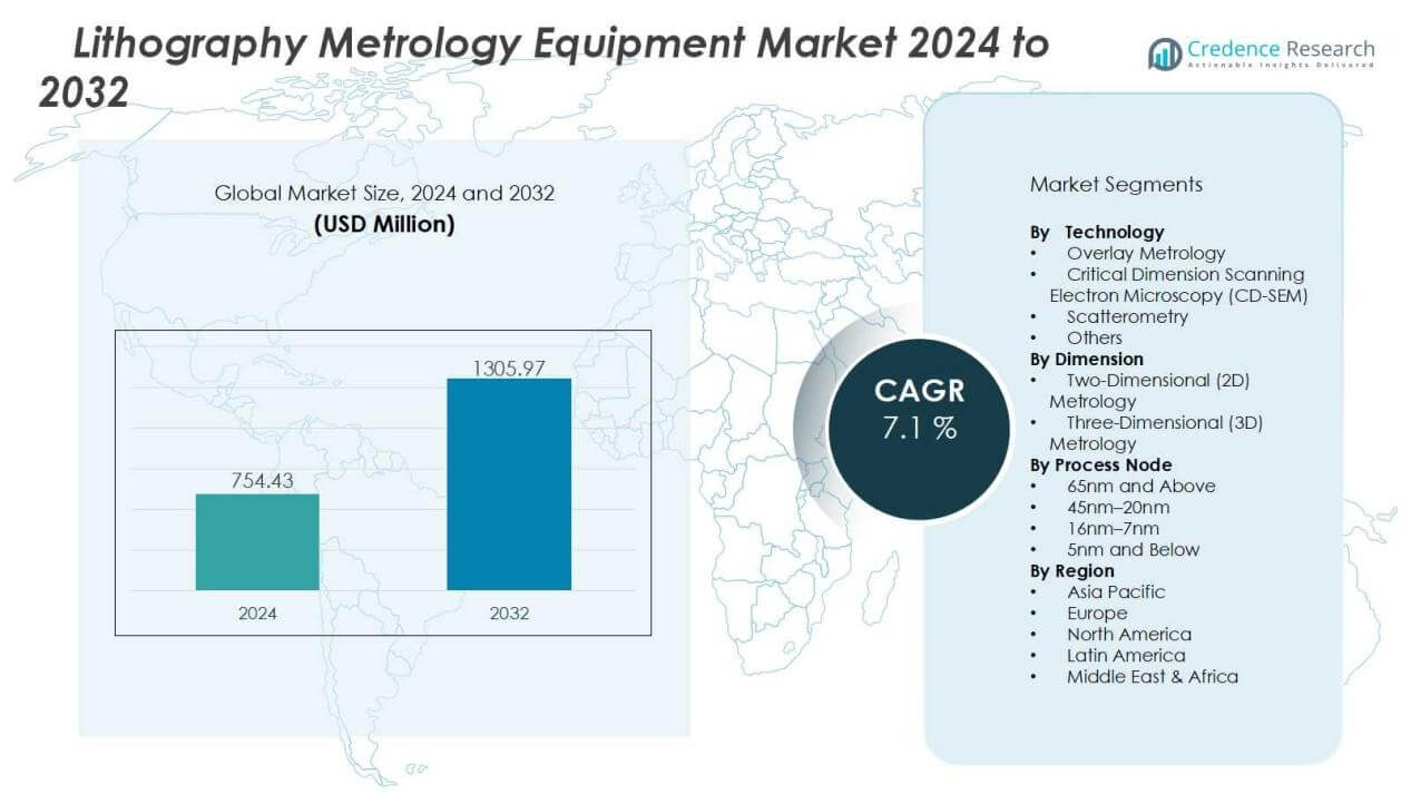
The Lithography Metrology Equipment Market size was valued at USD 754.43 million in 2024 and is anticipated to reach USD 1305.97 million by 2032, at a CAGR of 7.1 % during the forecast period.
| REPORT ATTRIBUTE |
DETAILS |
| Historical Period |
2020-2023 |
| Base Year |
2024 |
| Forecast Period |
2025-2032 |
| Lithography Metrology Equipment Market Size 2024 |
USD 754.43 Million |
| Lithography Metrology Equipment Market, CAGR |
7.1% |
| Lithography Metrology Equipment Market Size 2032 |
USD 1305.97 Million |
Key drivers of the lithography metrology equipment market include the rapid growth of the semiconductor sector, increasing complexity of integrated circuits, and the surge in consumer electronics and data-driven applications. The demand for 5G, AI, IoT, and high-performance computing devices is accelerating the adoption of advanced metrology solutions. Equipment providers are also innovating in overlay control, CD-SEM, and scatterometry technologies to ensure higher accuracy, reduce process variations, and meet stringent design rules.
Regionally, Asia Pacific dominates the lithography metrology equipment market due to its strong semiconductor manufacturing base in countries like Taiwan, South Korea, and China. North America follows, driven by R&D investments and the presence of key semiconductor players. Europe contributes through advanced lithography technology leadership, while emerging regions in Latin America and the Middle East are gradually increasing their adoption to support growing electronics demand.
 Market Insights:
- The lithography metrology equipment market was valued at USD 754.43 million in 2024 and is projected to reach USD 1305.97 million by 2032, growing at a CAGR of 7.1%.
- Rising demand for semiconductor miniaturization and nodes below 5nm drives adoption of advanced metrology tools to maintain precision and yield.
- Growth in consumer electronics, 5G, AI, and IoT applications increases the need for high-performance chips, boosting demand for inspection equipment.
- Expanding semiconductor fabrication capacity in Asia Pacific and North America creates sustained demand for metrology systems to ensure production quality.
- Advancements in scatterometry, CD-SEM, and overlay metrology technologies enhance process control, reduce variability, and support yield optimization.
- High equipment costs and integration complexity pose challenges for smaller fabs, limiting adoption in certain regions and slowing market penetration.
- Asia Pacific led with 54% share in 2024, followed by North America at 26% and Europe at 15%, supported by strong manufacturing and technology leadership.
Access crucial information at unmatched prices!
Request your sample report today & start making informed decisions powered by Credence Research Inc.!
Download Sample
Market Drivers:
Rising Demand from Semiconductor Miniaturization and Advanced Node Scaling:
The lithography metrology equipment market is strongly driven by the need for semiconductor miniaturization. Advanced nodes below 5nm require precise metrology tools to maintain accuracy and production yields. It supports manufacturers in controlling overlay errors and critical dimensions in increasingly complex designs. The trend toward smaller, more powerful chips sustains steady demand for advanced metrology equipment.
- For instance, in August 2022 ASML demonstrated on-product overlay accuracy of 2 nm for 5 nm generation devices.
Growth in Consumer Electronics, 5G, and AI Applications:
Expanding use of smartphones, tablets, and connected devices boosts the need for advanced chips. The lithography metrology equipment market benefits from this demand, as accuracy in patterning is essential for performance. Emerging technologies such as 5G, artificial intelligence, and IoT place further pressure on chipmakers to adopt high-end inspection tools. It creates a cycle of innovation and investment across the semiconductor value chain.
- For Instances, KLA-Tencor (now KLA Corporation) introduced the ATL (Accurate Tunable Laser) overlay metrology system that utilized tunable laser technology to achieve a 1 nm resolution in measuring layer alignment across advanced logic wafers.
Rising Investments in Semiconductor Manufacturing Capacity Expansion:
Global investments in wafer fabrication plants are increasing, especially in Asia Pacific and North America. The lithography metrology equipment market gains from this trend since fabs require precise inspection and measurement tools at every stage. Governments and private firms are investing billions in expanding semiconductor capacity to secure supply chains. It ensures sustained demand for metrology systems that maintain quality and efficiency in production.
Advancements in Metrology Technologies for Yield Optimization:
Continuous innovation in scatterometry, CD-SEM, and overlay metrology enhances precision and process control. The lithography metrology equipment market grows with these advancements, which help reduce variability and improve yields. Equipment providers are integrating AI and automation to deliver faster, more accurate results. It supports manufacturers in managing cost pressures while meeting the growing complexity of next-generation chips.
Market Trends:
Integration of Artificial Intelligence and Automation in Metrology Solutions:
The lithography metrology equipment market is witnessing strong adoption of artificial intelligence and automation across inspection and measurement systems. Manufacturers are deploying AI-driven analytics to detect defects, predict failures, and optimize process control with higher efficiency. Automation reduces operator dependency, enabling faster and more accurate metrology in high-volume semiconductor production. It improves productivity and lowers the risk of human error while supporting advanced node requirements. The combination of AI and machine learning ensures better overlay accuracy and critical dimension monitoring. This trend is expected to reshape how semiconductor fabs maintain yield and quality control.
- For instance, Applied Materials’ SEMVision G6 employs AI-driven analytics, utilizing Purity ADC machine learning algorithms for exceptional defect classification accuracy. This enables up to 100% faster throughput, minimizing human error and boosting productivity in high-volume semiconductor production
Rising Focus on Advanced Packaging and EUV Lithography Applications:
The lithography metrology equipment market is also shaped by the growing adoption of advanced packaging and extreme ultraviolet (EUV) lithography. Advanced packaging techniques demand precise metrology tools to manage multi-die integration and interconnect structures. EUV processes create new challenges in defect detection and overlay control, pushing the demand for next-generation metrology solutions. It drives innovation in scatterometry, SEM, and hybrid metrology platforms. The focus on heterogeneous integration and shrinking feature sizes further accelerates demand for highly accurate tools. This trend strengthens the importance of metrology as a critical enabler of advanced semiconductor manufacturing.
- For Instances, a KLA Archer overlay metrology system can achieve sub-2 nm intra-field overlay measurement accuracy (\(3\sigma \)) on EUV-exposed masks after advanced compensation techniques are applied. This metrology precision is essential for manufacturing today’s advanced chips, which have overlay budgets significantly tighter than the 4.5 nm target for older 32 nm nodes
Market Challenges Analysis:
High Cost of Advanced Equipment and Complexity of Integration:
The lithography metrology equipment market faces a significant challenge due to the high cost of advanced systems. Next-generation tools with AI, EUV, and automation features require heavy capital investments, which limit adoption among smaller fabs and emerging players. It creates a barrier to entry and slows widespread deployment in the global supply chain. Integrating these tools into existing production lines also adds complexity, requiring skilled technicians and advanced infrastructure. The cost burden is further intensified by continuous upgrades to keep pace with shrinking nodes. This financial and technical challenge restricts market penetration across certain regions and manufacturers.
Rapid Technological Changes and Short Product Life Cycles:
The lithography metrology equipment market is challenged by rapid technological evolution and short product life cycles. Equipment designed for current process nodes often becomes outdated within a few years as the industry advances toward smaller geometries. It pressures manufacturers to continuously innovate, increasing R&D expenses and operational risks. The fast pace of development also creates supply chain stress, as vendors must balance innovation with reliability and scalability. Limited standardization across regions and fabs further complicates adoption. This dynamic environment places heavy demands on both suppliers and end users to remain competitive.
Market Opportunities:
Expansion of Semiconductor Manufacturing and Government Incentives:
The lithography metrology equipment market has strong opportunities from expanding semiconductor manufacturing capacity worldwide. Governments in North America, Europe, and Asia Pacific are offering incentives to boost local chip production and reduce supply chain risks. It supports the deployment of advanced metrology systems in new and upgraded fabs. The shift toward self-sufficiency in semiconductor supply creates stable, long-term demand for inspection and measurement tools. Equipment vendors can benefit by forming partnerships with governments and foundries to align with capacity expansion projects. This wave of investment opens significant growth potential for suppliers with advanced and scalable solutions.
Rising Demand from Emerging Applications and Advanced Packaging:
The lithography metrology equipment market also benefits from new opportunities driven by emerging applications. The growth of electric vehicles, AI accelerators, and high-performance computing requires advanced chips with precise structures. It increases reliance on metrology to ensure accuracy in production. Advanced packaging techniques, such as 3D stacking and heterogeneous integration, require more sophisticated inspection and control systems. Vendors that offer hybrid metrology platforms and AI-enabled tools can capture new demand from these segments. Expanding applications beyond traditional consumer electronics strengthen the market’s long-term growth prospects.
Market Segmentation Analysis:
By Technology:
The lithography metrology equipment market is segmented by technologies such as overlay metrology, critical dimension scanning electron microscopy (CD-SEM), and scatterometry. Overlay metrology leads due to its vital role in managing alignment precision during advanced node production. CD-SEM remains important for high-resolution imaging and accurate measurement of nanoscale structures. Scatterometry gains traction as it enables fast, non-destructive measurements suitable for high-volume manufacturing. It ensures effective process control in increasingly complex chip designs.
- For instance, EV Group’s new EVG®40 D2W overlay metrology system achieves 100 percent overlay measurement on every die at up to 15 times higher throughput than previous industry standards, significantly enhancing manufacturing efficiency in 2025.
By Dimension:
The market is divided into two-dimensional (2D) and three-dimensional (3D) metrology systems. 2D metrology dominates traditional semiconductor manufacturing, where planar designs remain common. However, demand for 3D metrology is rising due to advanced packaging and 3D NAND memory production. It provides accurate measurement of complex structures such as multi-layered and stacked devices. Growing adoption of heterogeneous integration further drives this segment forward.
- For instance: KLA-Tencor’s Surfscan SP3, launched in July 2011, generates ~100 megapixel full-wafer SURFmonitor haze maps for sub-nanometer defect detection.
By Process Node:
The market is segmented by process nodes including 65nm and above, 45nm–20nm, 16nm–7nm, and 5nm and below. Equipment demand is strongest in the 5nm and below category, where precision requirements are highest. The 16nm–7nm segment also holds significant share, driven by widespread adoption across data centers and mobile applications. Larger nodes such as 45nm–20nm continue to serve legacy systems and automotive electronics. It reflects the balance between next-generation innovation and stable demand from mature applications.
Segmentations:
By Technology:
- Overlay Metrology
- Critical Dimension Scanning Electron Microscopy (CD-SEM)
- Scatterometry
- Others
By Dimension:
Two-Dimensional (2D) Metrology
- Three-Dimensional (3D) Metrology
By Process Node:
- 65nm and Above
- 45nm–20nm
- 16nm–7nm
- 5nm and Below
By Region:
- North America
- Europe
- Germany
- France
- U.K.
- Italy
- Spain
- Rest of Europe
- Asia Pacific
- China
- Japan
- India
- South Korea
- South-east Asia
- Rest of Asia Pacific
- Latin America
- Brazil
- Argentina
- Rest of Latin America
- Middle East & Africa
- GCC Countries
- South Africa
- Rest of the Middle East and Africa
Regional Analysis:
Asia Pacific:
Asia Pacific held 54% market share in the lithography metrology equipment market in 2024, supported by Taiwan, South Korea, and China. The region dominates due to its extensive semiconductor fabrication capacity and investments in advanced node production. It benefits from leading foundries that continuously expand capacity to meet global chip demand. Government-backed initiatives in China and South Korea further accelerate adoption of advanced metrology tools. Japan also plays a role with strong expertise in precision equipment and materials. The growing need for consumer electronics, AI devices, and automotive chips strengthens demand for advanced metrology in the region.
North America:
North America accounted for 26% market share in the lithography metrology equipment market in 2024, driven by the U.S. semiconductor industry. The region benefits from extensive R&D investments and the presence of major technology firms. It gains momentum from government programs supporting domestic chip manufacturing under strategic initiatives. Advanced lithography and metrology R&D hubs in the U.S. ensure technology leadership. The growing role of AI, 5G, and cloud computing fuels demand for accurate metrology systems. It remains a critical market due to strong integration of innovation and manufacturing.
Europe:
Europe captured 15% market share in the lithography metrology equipment market in 2024, supported by its strong expertise in lithography technology. The Netherlands plays a leading role with advanced equipment providers that set global standards. It benefits from collaborations between research institutions and industry to advance EUV and metrology innovation. Germany and France also contribute through investments in advanced electronics and automotive chips. The region focuses on securing semiconductor supply chains and strengthening competitiveness. It continues to expand demand for high-precision metrology tools across strategic industries.
Shape Your Report to Specific Countries or Regions & Enjoy 30% Off!
Key Player Analysis:
- Applied Materials, Inc.
- ASML
- Camtek
- Hitachi High-Tech Corporation
- KLA Corporation
- Lasertec Corporation
- Nova Ltd.
- Onto Innovation
- SCREEN Semiconductor Solutions Co., Ltd.
- Thermo Fisher Scientific Inc.
Competitive Analysis:
The lithography metrology equipment market is highly competitive, driven by innovation and continuous technology upgrades. Key players include Applied Materials, Inc., ASML, Camtek, Hitachi High-Tech Corporation, KLA Corporation, Lasertec Corporation, Nova Ltd., and Onto Innovation. These companies compete on precision, speed, and integration capabilities across advanced semiconductor production. It emphasizes R&D investments to address the challenges of smaller nodes and complex chip architectures. Strategic collaborations with leading foundries and research institutions strengthen market presence. Vendors are focusing on hybrid metrology, AI-driven analytics, and EUV-compatible solutions to secure leadership. The competitive landscape highlights a balance between global technology leaders and specialized firms delivering niche solutions.
Recent Developments:
- In March 2025, Hitachi High-Tech Corporation completed the operation of a new semiconductor manufacturing equipment production facility in the Kasado area, increasing production capacity using digitalized and automated lines while aiming for carbon neutrality.
- In February 2025, Nova Ltd. completed the acquisition of Sentronics Metrology GmbH, a German wafer metrology tools provider, expanding its metrology portfolio.
Report Coverage:
The research report offers an in-depth analysis based on Technology, Dimension, Process Node and Region. It details leading Market players, providing an overview of their business, product offerings, investments, revenue streams, and key applications. Additionally, the report includes insights into the competitive environment, SWOT analysis, current Market trends, as well as the primary drivers and constraints. Furthermore, it discusses various factors that have driven Market expansion in recent years. The report also explores Market dynamics, regulatory scenarios, and technological advancements that are shaping the industry. It assesses the impact of external factors and global economic changes on Market growth. Lastly, it provides strategic recommendations for new entrants and established companies to navigate the complexities of the Market.
Future Outlook:
- The lithography metrology equipment market will see rising demand from advanced node scaling below 3nm.
- It will gain momentum from the expansion of semiconductor fabs in Asia Pacific and North America.
- The market will benefit from government incentives and funding programs supporting domestic chip manufacturing.
- It will experience higher adoption of AI-driven metrology tools for faster and more accurate process control.
- The market will expand with growing demand from applications such as electric vehicles and high-performance computing.
- It will witness stronger integration of hybrid metrology platforms to handle complex semiconductor structures.
- The market will evolve with continuous innovation in scatterometry, SEM, and overlay metrology technologies.
- It will face increasing importance of advanced packaging solutions requiring precise inspection and measurement systems.
- The market will strengthen through partnerships between equipment vendors, foundries, and technology firms.
- It will remain critical in ensuring yield optimization and reliability in next-generation semiconductor manufacturing.


