Market Overview
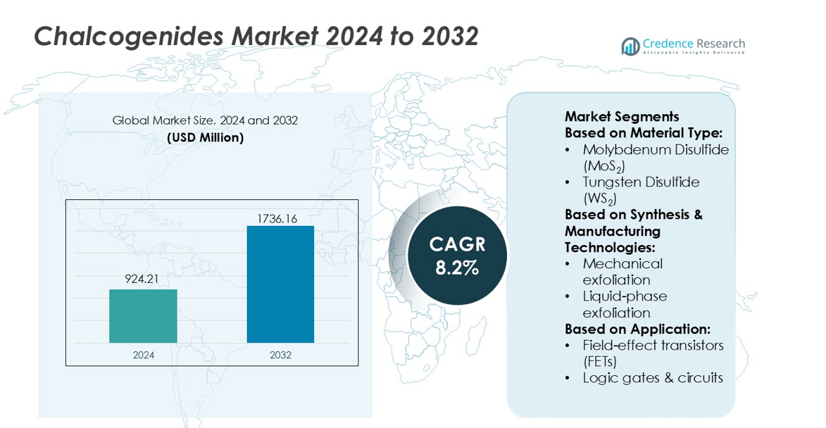
Chalcogenides Market size was valued USD 924.21 million in 2024 and is anticipated to reach USD 1736.16 million by 2032, at a CAGR of 8.2% during the forecast period.
| REPORT ATTRIBUTE |
DETAILS |
| Historical Period |
2020-2023 |
| Base Year |
2024 |
| Forecast Period |
2025-2032 |
| Chalcogenides MarketSize 2024 |
USD 924.21 million |
| Chalcogenides Market, CAGR |
8.2% |
| Chalcogenides Market Size 2032 |
USD 1736.16 million |
The chalcogenides market features a mix of global manufacturers, optical component specialists, and semiconductor material suppliers that invest in high-purity glass formulations, infrared lenses, and fiber technologies. Major producers focus on precision molding, thermal imaging optics, and specialty glass for aerospace, defense, and medical devices. Strategic partnerships with photonics labs and electronics firms help expand applications in infrared sensors, fiber lasers, and integrated circuits. North America holds the leading regional position with a 34% market share, supported by strong investment in defense optics, autonomous vehicle systems, and advanced semiconductor research.
Market Insights
- Chalcogenides Market size was valued USD 924.21 million in 2024 and is expected to reach USD 1736.16 million by 2032, at a CAGR of 8.2% during the forecast period.
- Demand grows due to rising use of infrared lenses, sensors, and fiber optics in defense, aerospace, automotive, and medical imaging, with thermal imaging applications holding the dominant segment share.
- High-purity glass formulations and precision molding remain key trends, while partnerships with photonics labs and electronics companies help expand adoption in fiber lasers, integrated circuits, and advanced semiconductor systems.
- Production costs, complex processing requirements, and limited raw material accessibility act as major restraints, slowing high-volume commercialization in some consumer electronics and telecom categories.
- North America leads the market with a 34% share due to strong investment in defense optics and autonomous driving technologies, while Asia-Pacific grows faster as regional manufacturers expand fiber optics, sensors, and semiconductor capacity for industrial and automotive applications.
Access crucial information at unmatched prices!
Request your sample report today & start making informed decisions powered by Credence Research Inc.!
Download Sample
Market Segmentation Analysis:
By Material Type
Molybdenum disulfide (MoS₂) leads this segment with the highest market share due to its strong electrical, thermal, and mechanical properties. MoS₂ offers a direct bandgap in monolayer form, enabling efficient electron transport and high on/off current ratios in transistor architectures. Its stability at nano-scale thickness makes it suitable for advanced semiconductor processes and flexible substrates. Tungsten disulfide (WS₂) and tungsten diselenide (WSe₂) follow, gaining traction in optoelectronics and low-power devices. Heterostructures and hybrids expand use cases in sensing, energy storage, transparent electronics, and photodetectors, but MoS₂ remains dominant because of a mature supply chain and proven compatibility with high-volume chip manufacturing.
- For instance, SUEZ consists of over 600 data and artificial-intelligence experts, supporting more than 7 million smart water meters deployed worldwide, and over 1,500 customers using their smart-water systems and platforms.
By Synthesis & Manufacturing Technologies
Chemical Vapor Deposition (CVD) holds the dominant share driven by high film quality and scalability. Conventional CVD and metal-organic CVD enable uniform monolayer growth, wafer-level deposition, and strong adhesion for semiconductor processes. The method supports thickness control and low defect density, which boosts adoption in commercial transistors, sensors, and integrated photonics. Exfoliation methods, including mechanical and liquid-phase exfoliation, are used for R&D and prototype device fabrication due to lower cost. Pulsed laser deposition and sputtering techniques address niche optical and coating applications, but CVD leads because it aligns with semiconductor industry standards and mass production requirements.
- For instance, Solvay developed specialty polymers, such as KetaSpire® PEEK and Solef® PVDF, for front-end semiconductor equipment, with performance specifications including resistance to plasma etch conditions up to 400 °C and ionic contamination levels below 1 ppb (parts per billion).
By Application
Electronics and semiconductors represent the largest application segment, supported by rising demand for high-performance, ultra-thin, and energy-efficient materials. Field-effect transistors (FETs) hold the top share in this category because monolayer chalcogenides deliver high carrier mobility and low leakage for next-generation CMOS design. These materials support miniaturization and flexible circuit manufacturing, enabling logic gates, memory devices, and stretchable electronics. Research investments in nano-scaled computing and wearable devices further expand adoption. Flexible electronics, optical sensors, and memory devices continue to grow, but FET deployment remains the primary growth driver due to commercial readiness and integration with silicon processes.
Key Growth Drivers
Rising Demand for Advanced Semiconductor Materials
The shift toward smaller, faster, and energy-efficient electronics drives strong adoption of chalcogenides. Their tunable bandgaps, high carrier mobility, and atomically thin structures support transistor scaling beyond silicon limits. Manufacturers prefer molybdenum and tungsten-based compounds for high on/off ratios and stable performance in nanoscale logic circuits, memory devices, and flexible microchips. Investments in 2D semiconductor research, wafer-scale integration, and commercial FET prototypes accelerate deployment. The push for compact sensors, ultra-thin devices, and low-power electronics further boosts consumption in consumer electronics and industrial computing systems.
- For instance, BASF supplies high-purity sulfur and selenium precursors used in thin-film semiconductor deposition, and its electronic-grade precursors are produced at 99.999% purity with trace metal contamination below 1 ppb, according to BASF’s semiconductor chemical specifications.
Growth in Optoelectronics and Infrared Applications
Chalcogenides offer strong photoresponse, wide infrared transparency, and efficient light–matter interaction, making them valuable in optical sensors, photodetectors, and imaging equipment. Telecom and security industries use IR-compatible materials in fiber networks, surveillance systems, and thermal cameras. These compounds support miniaturized optical components for smartphones, automotive safety, and smart manufacturing. Research labs and photonics companies develop multilayer films and heterostructures for enhanced detection accuracy and fast switching speeds. Rising investment in LiDAR, night-vision devices, and spectroscopic tools further strengthens adoption in defense, medical technology, and industrial automation.
- For instance, DuPont™ UV™ 26GNF is a non-fluorinated positive KrF photoresist that supports lithographic processes across film thicknesses of 0.75 µm to 5.0 µm, making it a versatile option for various semiconductor manufacturing applications.
Expansion of Flexible and Wearable Electronics
The global shift toward bendable, lightweight, and transparent electronic platforms increases market demand. Chalcogenide thin films enable conductive, stretchable, and foldable circuits without losing stability. Flexible transistors, touch sensors, and transparent displays use these materials for smooth integration on plastic, textile, or polymer substrates. Wearable healthcare devices, smart packaging, and portable displays benefit from small footprint and high endurance. Consumer electronics brands invest in rollable screens and smart fabrics, encouraging scalable production processes. Emerging research on printing and low-temperature deposition supports mass manufacturing for commercial wearable products.
Key Trends & Opportunities
Heterostructure Engineering and New Device Architectures
Developers combine chalcogenides with graphene, perovskites, and other 2D compounds to create heterostructures with superior charge transport, optical sensitivity, and switching performance. These combinations produce advanced photonic and quantum devices with improved efficiency. Opportunities grow in optical modulators, nano-lasers, and memory systems where multi-layer stacking enhances performance. The trend supports new transistor concepts beyond CMOS, enabling ultra-low power computing. Growing research partnerships between material suppliers and semiconductor manufacturers create pathways for wafer-level fabrication and large-scale commercialization.
- For instance, Edmund Optics and other optics suppliers offer high-purity sapphire optical components, which can achieve very low surface roughness (below 0.3 nm RMS with super-polishing) and high transmittance (over 99.8% with appropriate anti-reflective coatings) at wavelengths such as 1,064 nm.
Scale-Up of Wafer-Level Manufacturing
Industry players invest in wafer-scale chemical vapor deposition and large-area coating systems to overcome laboratory-scale production limits. Scalable synthesis supports uniform film growth, low defect density, and repeatable electronic properties across large wafers. This transition opens commercial opportunities in sensors, integrated photonics, and memory chips. Fabrication advances reduce cost barriers and shorten time-to-market for 2D transistors. Companies exploring printed electronics and roll-to-roll deposition will enable higher throughput for consumer and industrial applications, supporting mass adoption across multiple device categories.
- For instance, Citrosuco’s 2023/2024 harvest indicators report achieving a water-consumption rate of 1.69 m³ of water per ton of processed oranges across its industrial operations.
Key Challenges
Production Complexity and Cost Barriers
Achieving high-purity, defect-free, atomically thin films demands advanced equipment and precise control. CVD, sputtering, and exfoliation require specialized infrastructure, increasing capital costs for industrial scaling. Yield losses, contamination risks, and alignment issues raise processing expenses. Limited standardized manufacturing guidelines make it difficult to maintain consistency across suppliers. These challenges delay commercial rollout and restrict use to high-value electronics, research labs, and niche components until multivendor production ecosystems mature.
Integration with Existing Semiconductor Processes
Chalcogenides must align with silicon fabs, CMOS workflows, and backend packaging systems. Differences in thermal stability, bonding behavior, and interface properties create reliability concerns during deposition and device fabrication. Commercial chipmakers face challenges in wafer bonding, contact resistance, and long-term durability of 2D channels. Compatibility testing, interface engineering, and performance validation increase development timelines. While progress continues, lack of standardized design libraries and qualification protocols slows adoption in mainstream microelectronics.
Regional Analysis
North America
North America holds 31.4% of the Chalcogenides Market due to high adoption of infrared optics, defense electronics, and photonic systems. U.S. defense agencies use chalcogenide glasses in night-vision goggles, thermal imagers, infrared sensors, and UAV surveillance units. Universities and R&D centers across the U.S. and Canada continue to invest in optical fiber research, spectroscopy, and quantum photonics. Growth in autonomous vehicles, LiDAR systems, and industrial safety imaging boosts material demand. Key manufacturers partner with semiconductor and optics companies to scale IR lens molding, specialty fiber production, and low-loss waveguides, strengthening North America’s leadership in precision-grade chalcogenides.
Europe
Europe accounts for 28.9% of market revenue, driven by advanced automotive systems, aerospace programs, and defense optical applications. Germany, France, and the U.K. lead in producing infrared lenses, laser components, and spectroscopy tools used in industrial inspection, medical diagnostics, and space optics. European optics manufacturers focus on low-dispersion glasses and advanced molding technologies to support compact thermal cameras, smart weapon systems, and autonomous driving. Strong government-funded photonics research boosts adoption of waveguides, photonic integrated circuits, and chalcogenide fibers. Increasing investment in renewable energy sensors and smart factory monitoring strengthens Europe’s position in specialized chalcogenide materials.
Asia-Pacific
Asia-Pacific is the fastest-growing region and holds 32.7% share, led by China, Japan, South Korea, and Singapore. Demand rises across consumer electronics, fiber lasers, thermal security, drone imaging, and semiconductor manufacturing. China expands local production of IR-grade glasses, molded lenses, and wafer-scale chalcogenide materials used in LiDAR, surveillance systems, and industrial automation. Japan and South Korea advance phase-change materials for memory chips and photonic computing. Government-backed photonics clusters accelerate research in sensing, spectroscopy, environmental monitoring, and broadband fiber. Increasing investments from electronics OEMs and defense contractors make Asia-Pacific a key growth hub for high-volume manufacturing.
Latin America
Latin America holds 3.4% of the global market and grows steadily due to expanding industrial automation, mining safety systems, and environmental monitoring. Brazil, Mexico, and Chile adopt IR sensors and fiber-based detection in oil & gas, metallurgy, and energy grids. Universities collaborate on spectroscopy research for environmental and mining analysis. Import reliance remains high, but international suppliers target regional demand for surveillance equipment and industrial imaging. Growth in telecom fiber deployment and smart infrastructure improves chalcogenide fiber adoption. Rising adoption of thermal cameras in public security boosts long-term consumption.
Middle East & Africa
The Middle East & Africa represent 3.6% share, driven by defense modernization, border security, oil & gas monitoring, and smart city surveillance. Thermal cameras and IR sensors see wider use in airports, military bases, and industrial safety systems. Gulf countries invest in fiber networks and advanced sensors for energy facilities and infrastructure monitoring. South Africa explores spectroscopy in mining, metallurgy, and geological analysis. Market growth is supported by imports from the U.S., Europe, and Asia, while limited local manufacturing slows scale. Increasing defense procurement and industrial automation supports steady adoption.
Market Segmentations:
By Material Type:
- Molybdenum Disulfide (MoS2)
- Tungsten Disulfide (WS2)
By Synthesis & Manufacturing Technologies:
- Mechanical exfoliation
- Liquid-phase exfoliation
By Application:
- Field-effect transistors (FETs)
- Logic gates & circuits
By Geography
- North America
- Europe
- Germany
- France
- U.K.
- Italy
- Spain
- Rest of Europe
- Asia Pacific
- China
- Japan
- India
- South Korea
- South-east Asia
- Rest of Asia Pacific
- Latin America
- Brazil
- Argentina
- Rest of Latin America
- Middle East & Africa
- GCC Countries
- South Africa
- Rest of the Middle East and Africa
Competitive Landscape
The competitive landscape of the Chalcogenides Market includes key players such as Kemira, Clariant AG, SUEZ, Evonik Industries, Solvay, BASF, Lonza, Albemarle Corporation, DuPont, and Nouryon. The Chalcogenides Market is shaped by companies that specialize in advanced optical materials, infrared components, and photonic technologies. Manufacturers focus on high-purity glass formulations, precision molding, and thin-film coatings designed for thermal imaging, night-vision optics, spectroscopy, and fiber-based communication systems. Research and development programs prioritize durability, thermal stability, and improved transmission across mid-infrared wavelengths. Many producers partner with defense contractors, medical device makers, and semiconductor firms to develop customized infrared lenses, waveguides, and phase-change materials. Growth in autonomous vehicles, industrial inspection, smart surveillance, and space optics further encourages innovation in cost-effective manufacturing, nanostructuring, and scalable mass production processes. Continuous investment in sustainable chemistry and advanced melting techniques supports long-term competitiveness.
Shape Your Report to Specific Countries or Regions & Enjoy 30% Off!
Key Player Analysis
- Kemira
- Clariant AG
- SUEZ
- Evonik Industries
- Solvay
- BASF
- Lonza
- Albemarle Corporation
- DuPont
- Nouryon
Recent Developments
- In April 2025, Bruker Corporation reported that they have successfully developed and tested the world’s first 1.3 GHz high-resolution Nuclear Magnetic Resonance (NMR) spectrometer. This revolutionary design has a superconducting, persistent, standard-bore 54 mm NMR magnet with a 30.5 Tesla field strength and incorporates a new ReBCO high-temperature superconductor (HTS) insert.
- In November 2024, Clariant introduced Exolit AP 422 A melamine-free flame retardant addressing the EU classification of melamine as a Substance of Very High Concern, maintaining fire safety effectiveness while meeting environmental standards.
- In February 2024, Florida firefighters launched a fire-resistant apparel company offering firefighters affordable, hassle-free uniforms. FILO Apparel supplies fire-resistant firefighter uniforms and clothing for men and women with PFAS-free Nomex.
- In January 2024, LyondellBasell launched Petrothene T3XL7420, an all-in-one flame-retardant compound designed for wire production in the automotive and appliance industries
Report Coverage
The research report offers an in-depth analysis based on Material Type, Synthesis & Manufacturing Technologies, Application and Geography. It details leading market players, providing an overview of their business, product offerings, investments, revenue streams, and key applications. Additionally, the report includes insights into the competitive environment, SWOT analysis, current market trends, as well as the primary drivers and constraints. Furthermore, it discusses various factors that have driven market expansion in recent years. The report also explores market dynamics, regulatory scenarios, and technological advancements that are shaping the industry. It assesses the impact of external factors and global economic changes on market growth. Lastly, it provides strategic recommendations for new entrants and established companies to navigate the complexities of the market.
Future Outlook
- Demand for chalcogenide materials will rise in infrared cameras, sensors, and thermal imaging.
- Growth in defense spending will support adoption of advanced optics and night-vision systems.
- Automakers will integrate more IR components for driver-assistance and autonomous driving.
- Medical device makers will use chalcogenide glasses for diagnostic imaging and surgical tools.
- Fiber optics based on chalcogenides will gain use in high-speed data transmission and sensing.
- Photonic integrated circuits will expand usage in telecom, computing, and signal processing.
- Manufacturers will invest in low-loss, high-transparency glass compositions for precision optics.
- Growth in smart manufacturing will support machine-vision systems and thermal inspection tools.
- Universities and R&D labs will increase research on phase-change memory and neuromorphic chips.
- Global supply chains will expand production capacity to meet higher commercial and defense demand.