| REPORT ATTRIBUTE |
DETAILS |
| Historical Period |
2020-2023 |
| Base Year |
2024 |
| Forecast Period |
2025-2032 |
| E Beam Wafer Inspection System Market Size 2024 |
USD 665.2 million |
| E Beam Wafer Inspection System Market, CAGR |
6.86% |
| E Beam Wafer Inspection System Market Size 2032 |
USD 1,129.6 million |
Market Overview
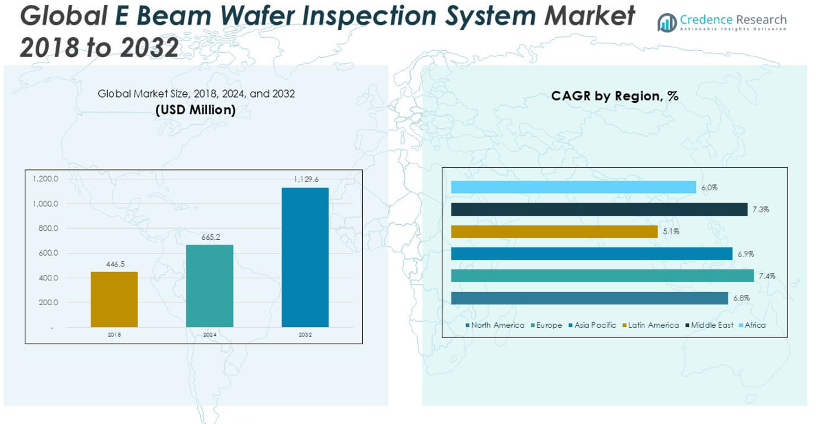
The E Beam Wafer Inspection System Market was valued at USD 446.5 million in 2018 and grew to USD 665.2 million in 2024. It is anticipated to reach USD 1,129.6 million by 2032, reflecting a compound annual growth rate (CAGR) of 6.86% during the forecast period.
The E Beam Wafer Inspection System Market is driven by the rising demand for advanced semiconductor devices and the growing complexity of integrated circuits, which require highly precise defect detection solutions. Increasing adoption of smaller process nodes and the transition toward 3D NAND and FinFET architectures have intensified the need for high-resolution inspection tools capable of identifying minute defects at the nanoscale. Additionally, the push for higher yield and production efficiency among semiconductor manufacturers supports robust investment in e-beam inspection technologies. On the trends front, the market is witnessing rapid integration of artificial intelligence and machine learning algorithms to improve defect classification and inspection accuracy. The expansion of foundry capacities, especially in Asia-Pacific, and the ongoing shift to advanced packaging further propel market growth. However, the high cost and operational complexity of these systems present challenges to widespread adoption among smaller manufacturers.
The E Beam Wafer Inspection System Market demonstrates strong geographical diversity, with major growth concentrated in North America, Europe, and Asia Pacific. Asia Pacific leads due to significant investments in semiconductor fabrication across China, Japan, South Korea, and Taiwan, supported by robust demand from consumer electronics and advanced manufacturing sectors. North America and Europe remain important markets, driven by established semiconductor industries, research infrastructure, and innovation in inspection technologies. Latin America, the Middle East, and Africa show emerging potential as local manufacturing capabilities expand. Key players such as KLA-Tencor Corporation, ASML Holding NV, and Applied Materials, Inc. drive market innovation through continuous development of high-resolution inspection systems, advanced automation, and integrated AI solutions. These companies maintain strong global footprints and partner with leading chip manufacturers to address evolving process requirements and enhance semiconductor quality assurance worldwide.
Market Insights
- The E Beam Wafer Inspection System Market was valued at USD 446.5 million in 2018, reached USD 665.2 million in 2024, and is projected to hit USD 1,129.6 million by 2032, with a CAGR of 6.86% during the forecast period.
- Market growth is supported by the rising complexity of semiconductor devices and the need for precise defect detection at advanced process nodes.
- Increasing adoption of automation, AI, and machine learning in inspection workflows is transforming the way manufacturers identify and classify wafer defects.
- Leading companies such as KLA-Tencor Corporation, ASML Holding NV, and Applied Materials, Inc. are driving the market by launching high-resolution, smart inspection systems to support next-generation chip production.
- High capital investment requirements and operational complexity pose key restraints for widespread market adoption, especially among smaller and mid-sized semiconductor manufacturers.
- Asia Pacific leads the market in terms of revenue and expansion, with North America and Europe following closely behind, fueled by large-scale investments in R&D and advanced fab infrastructure.
- The market outlook remains positive, with emerging opportunities in automotive, IoT, and advanced packaging segments, along with the ongoing expansion of foundry capacity in both established and developing regions.
Market Drivers
Advancing Semiconductor Miniaturization Accelerates Demand for High-Precision Inspection
The E Beam Wafer Inspection System Market benefits significantly from the rapid miniaturization of semiconductor devices and the push for next-generation chip designs. Shrinking process nodes and evolving architectures such as FinFET and 3D NAND demand inspection tools capable of detecting extremely small defects. The industry’s drive for higher circuit densities increases the risk of minute process anomalies, creating a greater reliance on e-beam inspection systems for quality control. Manufacturers seek to minimize defectivity rates, and e-beam solutions offer the nanometer-level resolution required for advanced manufacturing nodes. This trend is reinforced by the need to maintain yield and reliability in high-value semiconductor wafers. The market continues to gain traction as chipmakers embrace leading-edge technologies.
- For instance, KLA Corporation’s eSL10 e-beam inspection system is capable of detecting bridge and missing contact defects as small as 10 nanometers, meeting the requirements of production at the 5nm and 3nm nodes.
Surging Investment in Production Yields and Cost Efficiency
Semiconductor manufacturers aim to maximize yield and reduce overall production costs, prompting greater adoption of e-beam wafer inspection systems. The market benefits from the rising emphasis on improving defect detection and preventing costly wafer scrap. Companies rely on these systems to achieve greater process stability and to optimize throughput during high-volume manufacturing. E-beam inspection supports in-line process control and root cause analysis, which directly impacts profitability for fabs and foundries. As manufacturers introduce more complex process steps, advanced inspection tools have become essential for safeguarding quality. It offers a cost-effective solution over time by reducing material losses and supporting process optimization initiatives.
- For instance, Applied Materials’ PROVision e-beam inspection system has enabled fabs to improve critical defect detection rates by up to 3 times compared to previous inspection methods.
Integration of Artificial Intelligence and Machine Learning for Enhanced Defect Detection
Recent advancements in artificial intelligence and machine learning have become key drivers for the E Beam Wafer Inspection System Market. AI-enabled systems analyze vast datasets generated during inspection and provide rapid defect classification and actionable insights. It enables semiconductor manufacturers to automate inspection workflows and improve overall accuracy. AI-driven pattern recognition allows for the early identification of subtle defect trends, supporting faster process improvements. The market sees increasing demand for e-beam systems with smart software integration to meet complex inspection requirements. Machine learning further refines inspection parameters, ensuring continuous performance enhancement.
Expansion of Foundry Capacity and Growth in Advanced Packaging Segments
Global expansion in foundry capacities, particularly across Asia-Pacific, strengthens demand for e-beam wafer inspection systems. Semiconductor manufacturers are increasing investments in new fabrication plants to meet rising demand for consumer electronics, automotive, and data center applications. The growth in advanced packaging techniques, such as wafer-level packaging and heterogeneous integration, also fuels market expansion. It plays a critical role in inspecting new package architectures, ensuring high-quality outputs for next-generation products. The market’s relevance continues to grow as advanced packaging adoption increases. Strategic investments in production infrastructure and technological upgrades further propel the market’s upward trajectory.
Market Trends
Increasing Adoption of Advanced Automation and Smart Manufacturing Practices
The E Beam Wafer Inspection System Market is witnessing a marked increase in the integration of advanced automation technologies within semiconductor manufacturing. Companies are deploying automated inspection workflows to boost throughput and achieve consistent, high-quality results across complex wafer production lines. It supports streamlined operations and reduces manual intervention, which minimizes error rates. Automated e-beam systems help manufacturers meet the demand for rapid defect detection and process optimization. Industry leaders are prioritizing investments in smart manufacturing to maintain competitiveness in a fast-evolving sector. The trend toward automated solutions aligns with the broader push for digital transformation in semiconductor fabs.
- For instance, ASML’s HMI eScan 1100 e-beam inspection tool achieves a throughput of up to 40 wafers per hour with fully automated recipe setup, reducing human intervention and maximizing production efficiency.
Proliferation of Artificial Intelligence and Deep Learning in Defect Analysis
Artificial intelligence and deep learning technologies are increasingly influencing the development of e-beam inspection tools. The E Beam Wafer Inspection System Market benefits from the integration of AI-based software that enables sophisticated defect classification and predictive maintenance capabilities. It empowers manufacturers to extract actionable insights from vast inspection datasets and refine their process controls in real time. AI-driven defect analysis improves accuracy and enhances the detection of previously unrecognized patterns. The deployment of machine learning models accelerates the speed and efficiency of inspection, making advanced defect review accessible at scale. The adoption of these digital technologies is reshaping industry standards for inspection performance.
- For instance, Hitachi High-Tech’s GS1000 e-beam system can classify over 1,200,000 defect images per hour with a classification accuracy above 95% using proprietary AI algorithms.
Shift Toward Higher Resolution and Multi-Beam E Beam Inspection Systems
The market is moving toward higher-resolution and multi-beam e-beam inspection systems to address the rising complexity of semiconductor devices. The E Beam Wafer Inspection System Market reflects growing demand for inspection tools that offer enhanced sensitivity and faster throughput without compromising accuracy. Multi-beam configurations enable parallel processing of multiple regions, reducing inspection cycle times. It meets the requirements of advanced process nodes and supports emerging chip architectures. Manufacturers view these innovations as critical for maintaining quality at scale. The transition to multi-beam and high-resolution systems signals a major evolution in defect detection technology.
Rising Focus on Cost-Effective and Scalable Inspection Solutions
Market participants are emphasizing the need for scalable, cost-effective inspection solutions in response to fluctuating demand and intense industry competition. The E Beam Wafer Inspection System Market is characterized by efforts to lower total cost of ownership and improve return on investment for semiconductor manufacturers. It supports adoption in both large-scale foundries and smaller specialty fabs. Manufacturers are seeking flexible systems that can adapt to diverse process requirements and future technology nodes. The trend favors modular solutions and service-based models that optimize operational efficiency. These developments are broadening market accessibility while sustaining quality and innovation standards.
Market Challenges Analysis
High Capital Investment and Operational Complexity Limits Market Penetration
The E Beam Wafer Inspection System Market faces significant barriers due to the high upfront capital investment required for procurement and installation. Advanced e-beam inspection systems demand substantial expenditure, making them less accessible for smaller semiconductor manufacturers or those in emerging regions. It often requires a long return on investment period, which can deter companies with limited financial resources. Operational complexity further intensifies challenges, as these systems require specialized expertise for calibration, maintenance, and data interpretation. Training and retaining qualified personnel to operate e-beam tools imposes additional costs. These factors collectively restrict the widespread adoption and limit market penetration among cost-sensitive segments.
Throughput Limitations and Integration Challenges Affect Productivity
Throughput limitations present a persistent challenge for the E Beam Wafer Inspection System Market, particularly in high-volume manufacturing environments. Single-beam systems can struggle to keep pace with the rapid cycle times demanded by leading-edge semiconductor fabs. It can create bottlenecks in inspection processes, potentially impacting overall productivity and yield rates. Integration with existing manufacturing execution systems and data platforms poses further technical challenges. Achieving seamless interoperability between e-beam inspection tools and automated wafer handling equipment often requires significant customization. These integration hurdles, along with the need for ongoing software and hardware updates, complicate deployment and raise operational costs.
Market Opportunities
Rising Demand for Advanced Nodes and Heterogeneous Integration Fuels New Growth Prospects
The E Beam Wafer Inspection System Market is positioned to capitalize on the rising adoption of advanced semiconductor nodes and heterogeneous integration techniques. Growth in demand for high-performance computing, AI chips, and next-generation consumer electronics creates new opportunities for precision inspection solutions. It plays a crucial role in quality assurance for devices produced on sub-5nm and sub-3nm process technologies, where traditional optical inspection methods reach their limits. Expansion of applications in automotive, 5G, and IoT further elevates the need for advanced e-beam systems. The market stands to benefit from semiconductor manufacturers’ willingness to invest in new inspection capabilities to secure yield and performance at cutting-edge nodes.
Emerging Markets and Customizable Solutions Drive Broader Adoption
Emerging markets in Asia-Pacific, Latin America, and Eastern Europe present promising opportunities for the E Beam Wafer Inspection System Market. Semiconductor fabrication capacity in these regions continues to expand, supported by public and private investment in local electronics and foundry sectors. It supports broader adoption of e-beam inspection through the development of more flexible, modular, and scalable solutions. Customizable systems allow manufacturers to adapt inspection processes to diverse wafer sizes, materials, and advanced packaging requirements. Increasing demand for cost-efficient and easily upgradable inspection platforms further expands market reach and strengthens growth prospects for global suppliers.
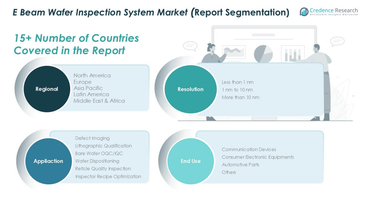
Market Segmentation Analysis:
By Resolution:
Systems offering less than 1 nm precision represent the pinnacle of defect detection capabilities, enabling manufacturers to identify the smallest process anomalies in advanced nodes. The 1 nm to 10 nm segment delivers high sensitivity for mainstream production environments, supporting a balance of cost-effectiveness and inspection accuracy. Systems with resolutions greater than 10 nm serve legacy process nodes and specialized applications, providing sufficient quality assurance where ultra-fine detection is less critical.
- For instance, the ZEISS AURIGA Crossbeam system achieves imaging resolution down to 0.9 nanometers at 15 kV accelerating voltage, allowing for reliable inspection at atomic-level precision.
By Application:
Defect imaging stands out as a leading segment due to its critical role in identifying, localizing, and categorizing process defects that impact wafer yield and device reliability. Lithographic qualification is gaining importance as manufacturers adopt next-generation lithography techniques and require stringent validation of critical layers. Bare wafer OQC/IQC supports quality control for incoming and outgoing wafers, allowing for the detection of contamination or surface defects before further processing. Wafer dispositioning leverages e-beam systems to make rapid go/no-go decisions that optimize production flow. Reticle quality inspection has become vital as photomask complexity grows, ensuring flawless mask transfer and minimizing downstream yield loss. Inspector recipe optimization provides manufacturers with the flexibility to adapt inspection strategies to evolving process requirements and maximize tool efficiency.
- For instance, Applied Materials’ PROVision e-beam platform has inspected over 100,000 wafers per month for defect imaging and lithography qualification in high-volume production environments.
By End-Use:
The communication devices segment leads market demand, driven by the proliferation of advanced smartphones, wireless infrastructure, and network equipment requiring stringent quality standards. Consumer electronic equipment manufacturers increasingly invest in e-beam inspection to support innovation in wearables, home devices, and personal electronics. Automotive parts constitute a fast-growing end-use category as vehicles incorporate more advanced semiconductor components for safety, connectivity, and electrification. The others segment covers industrial, medical, and emerging applications where specialized inspection needs continue to evolve. The segmentation structure ensures the E Beam Wafer Inspection System Market remains aligned with the semiconductor industry’s diverse and rapidly advancing requirements.
Segments:
Based on Resolution:
- Less than 1 nm
- 1 nm to 10 nm
- More than 10 nm
Based on Application:
- Defect Imaging
- Lithographic Qualification
- Bare Wafer OQC/IQC
- Wafer Dispositioning
- Reticle Quality Inspection
- Inspector Recipe Optimization
Based on End-Use:
- Communication Devices
- Consumer Electronic Equipments
- Automotive Parts
- Others
Based on the Geography:
- North America
- Europe
- UK
- France
- Germany
- Italy
- Spain
- Russia
- Belgium
- Netherlands
- Austria
- Sweden
- Poland
- Denmark
- Switzerland
- Rest of Europe
- Asia Pacific
- China
- Japan
- South Korea
- India
- Australia
- Thailand
- Indonesia
- Vietnam
- Malaysia
- Philippines
- Taiwan
- Rest of Asia Pacific
- Latin America
- Brazil
- Argentina
- Peru
- Chile
- Colombia
- Rest of Latin America
- Middle East
- UAE
- KSA
- Israel
- Turkey
- Iran
- Rest of Middle East
- Africa
- Egypt
- Nigeria
- Algeria
- Morocco
- Rest of Africa
Regional Analysis
North America E Beam Wafer Inspection System Market
North America E Beam Wafer Inspection System Market grew from USD 117.53 million in 2018 to USD 174.26 million in 2024 and is projected to reach USD 294.04 million by 2032, reflecting a compound annual growth rate (CAGR) of 6.8%. North America is holding a 26% market share. The region’s strength lies in its established semiconductor ecosystem, with the United States driving investments in R&D, advanced foundries, and AI-integrated inspection tools. Canada supports growth through collaborative innovation hubs and government incentives, while Mexico’s electronics assembly sector is driving demand for inspection solutions. The market benefits from a robust base of leading chip manufacturers and equipment suppliers, ensuring continuous demand for high-precision inspection systems.
Europe E Beam Wafer Inspection System Market
Europe E Beam Wafer Inspection System Market grew from USD 106.50 million in 2018 to USD 163.85 million in 2024 and is forecasted to reach USD 289.97 million by 2032, achieving a CAGR of 7.4%. Europe accounts for 25.7% market share. Germany and France lead the region’s adoption of e-beam inspection technology, supporting their strong automotive and industrial electronics sectors. The presence of world-class research institutions and a skilled workforce positions the region as a center for process innovation. Growth in the UK and the Netherlands is supported by investments in next-generation semiconductor fabs and packaging facilities. Europe’s regulatory focus on quality and sustainability strengthens demand for advanced inspection tools.
Asia Pacific E Beam Wafer Inspection System Market
Asia Pacific E Beam Wafer Inspection System Market grew from USD 146.77 million in 2018 to USD 219.04 million in 2024 and is estimated to reach USD 372.77 million by 2032, posting a CAGR of 6.9%. Asia Pacific leads with a 33% market share, making it the dominant region. China, Japan, South Korea, and Taiwan are key markets driving regional growth, supported by large-scale semiconductor fabrication plants and continuous investment in advanced manufacturing. The region’s demand is propelled by a strong consumer electronics industry and rapid adoption of new technologies. Government initiatives in China and India foster R&D and technology transfer, ensuring a favorable environment for market expansion. Asia Pacific’s position as the global semiconductor hub secures its leadership in e-beam inspection system deployment.
Latin America E Beam Wafer Inspection System Market
Latin America E Beam Wafer Inspection System Market grew from USD 39.21 million in 2018 to USD 53.33 million in 2024 and is set to reach USD 79.07 million by 2032, representing a CAGR of 5.1%. Latin America captures a 7% market share. Brazil and Mexico are principal contributors to market activity, leveraging their expanding electronics manufacturing bases and import of advanced semiconductor inspection solutions. The market is supported by local assembly and growing interest from multinational semiconductor companies. Strategic investments in manufacturing capacity and government-backed technology incentives are driving gradual adoption of e-beam systems. Latin America’s market is emerging, but increasing demand for consumer electronics and automotive parts will support future growth.
Middle East E Beam Wafer Inspection System Market
Middle East E Beam Wafer Inspection System Market grew from USD 27.55 million in 2018 to USD 41.99 million in 2024 and is expected to reach USD 73.42 million by 2032, reflecting a CAGR of 7.3%. The Middle East holds a 6.5% market share. Key countries such as Israel and the United Arab Emirates play leading roles, supported by innovation-driven policies and advanced R&D clusters. The market benefits from strategic partnerships with international semiconductor firms and a growing focus on electronics self-sufficiency. Demand is rising from sectors such as telecommunications and defense, driving further investments in high-precision inspection technologies.
Africa E Beam Wafer Inspection System Market
Africa E Beam Wafer Inspection System Market grew from USD 8.98 million in 2018 to USD 12.77 million in 2024 and is projected to reach USD 20.33 million by 2032, with a CAGR of 6.0%. Africa maintains a 1.8% market share. South Africa and Egypt are notable markets within the region, leveraging their expanding industrial base and increasing adoption of automation. The market remains at an early stage but receives support from government initiatives promoting electronics manufacturing and technology transfer. Investments in education and workforce training are laying the foundation for future growth. Africa presents untapped potential for market participants focused on long-term development.
Key Player Analysis
- ASML Holding NV
- Applied Materials, Inc.
- KLA-Tencor Corporation
- Lam Research Corporation
- NXP Semiconductors NV
- Taiwan Semiconductor Manufacturing Co., Ltd.
- Renesas Electronics Corporation
- Hitachi Ltd.
- Integrated Device Technology Inc.
Competitive Analysis
The E Beam Wafer Inspection System Market features a concentrated competitive landscape, dominated by established technology leaders such as KLA-Tencor Corporation, ASML Holding NV, Applied Materials, Inc., Hitachi Ltd., and Lam Research Corporation. These companies hold a commanding position through strong global distribution networks, robust R&D investments, and a deep understanding of semiconductor process requirements. KLA-Tencor excels in developing advanced e-beam platforms tailored to evolving process nodes and defect types, often setting industry standards for accuracy and reliability. Companies prioritize investments in research and development to enhance system sensitivity, throughput, and AI-based defect classification, ensuring their solutions align with the latest industry requirements. The market environment encourages strong collaboration between inspection system providers and semiconductor foundries, enabling the rapid adoption of advanced e-beam technologies in both established and emerging regions. Competitive strategies also include expanding product portfolios, offering comprehensive service and support packages, and targeting high-growth application segments such as automotive electronics and advanced packaging. Market participants continuously adapt to evolving customer demands, global supply chain challenges, and the need for cost-effective solutions, reinforcing the market’s dynamic and forward-looking character
Recent Developments
- In December 2023, Hitachi High-Tech Corporation, a leading provider of semiconductor manufacturing equipment and services announced the launch of a new high-precision electron beam metrology system. GT2000 is equipped with new detection systems for cutting-edge 3D semiconductor devices.
- in June 2022, Hitachi High-Tech Corporation also launched the Hitachi Dark Field Water Defect Inspection System. The DI2800 system is designed to detect defects on patterned wafers with high sensitivity and throughput.
- In 2022, ASML installed its first HMI eScan 1100 at a customer site. This marked the debut of the company’s first multi-beam (multielectron beam) wafer inspection system, designed for in-line yield improvement tasks such as voltage contrast and physical defect inspection.
Market Concentration & Characteristics
The E Beam Wafer Inspection System Market demonstrates a high degree of market concentration, with a small number of global players accounting for the majority of revenue and technology leadership. It is characterized by significant barriers to entry, including the need for advanced R&D capabilities, high capital investment, and specialized technical expertise. The market’s competitive environment revolves around continuous innovation in system resolution, throughput, and AI-driven defect classification. It features long product development cycles and strong emphasis on intellectual property protection, which helps incumbents sustain their leadership positions. Customer relationships tend to be long term, as semiconductor manufacturers rely on proven solutions and strong service support to minimize production risks. The market shows a strong alignment with the evolution of semiconductor process nodes and the increasing complexity of chip designs, making adaptability and technology integration essential characteristics.
Report Coverage
The research report offers an in-depth analysis based on Resolution, Application, End-Use and Geography. It details leading market players, providing an overview of their business, product offerings, investments, revenue streams, and key applications. Additionally, the report includes insights into the competitive environment, SWOT analysis, current market trends, as well as the primary drivers and constraints. Furthermore, it discusses various factors that have driven market expansion in recent years. The report also explores market dynamics, regulatory scenarios, and technological advancements that are shaping the industry. It assesses the impact of external factors and global economic changes on market growth. Lastly, it provides strategic recommendations for new entrants and established companies to navigate the complexities of the market.
Future Outlook
- Demand for sub-3nm wafer inspection drives further investment in high-resolution e-beam systems.
- Integration of AI and deep learning will improve defect classification accuracy and reduce inspection time.
- Multi-beam architectures will gain traction to balance high throughput with ultra-fine resolution.
- Modular system designs will offer scalable solutions tailored to diverse fab requirements.
- Adoption in automotive chip production will expand due to safety and reliability demands.
- Growth in advanced packaging use cases, including 2.5D and 3D stacking, will increase inspection complexity.
- Service-based models and leasing options will lower entry barriers for emerging fabs.
- Collaboration between inspection providers and foundries will accelerate technology customization.
- Regional fab expansions across Asia Pacific, the Middle East, and Latin America will open new markets.
- Standardization of inspection protocols will streamline global fab integration and quality assurance.


