Market Overview
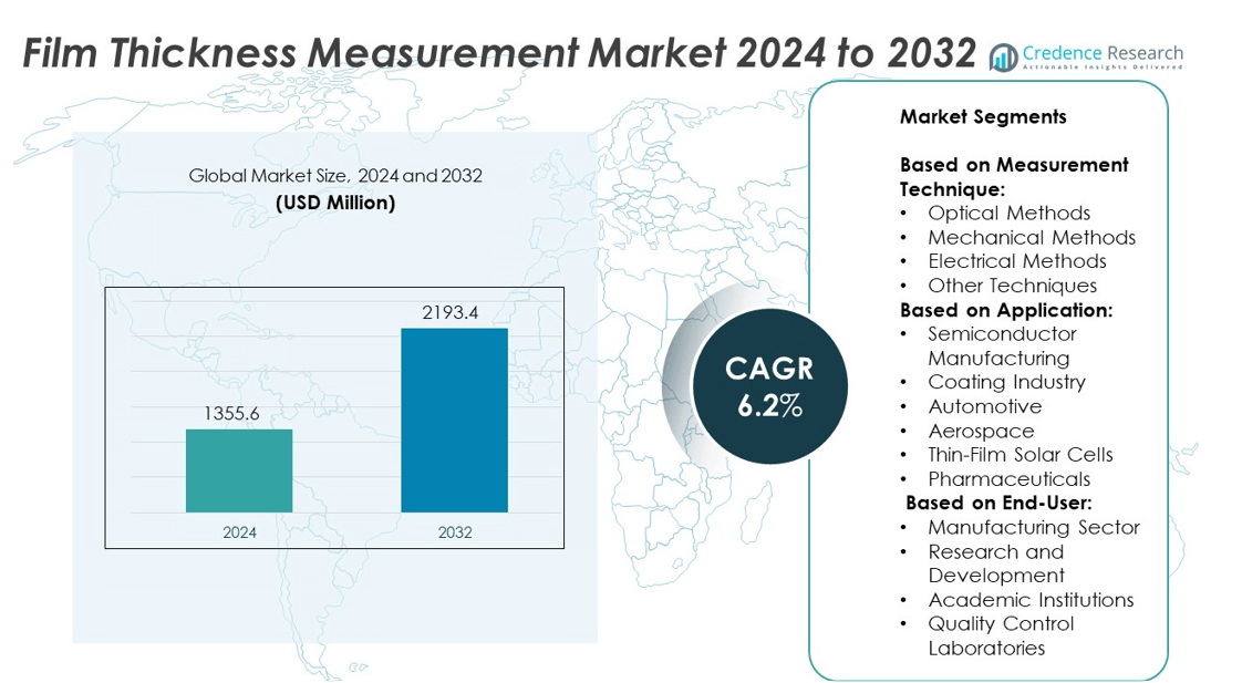
The Film Thickness Measurement Market size was valued at USD 1355.6 million in 2024 and is anticipated to reach USD 2193.4 million by 2032, registering a CAGR of 6.2% during the forecast period.
| REPORT ATTRIBUTE |
DETAILS |
| Historical Period |
2020-2023 |
| Base Year |
2024 |
| Forecast Period |
2025-2032 |
| Film Thickness Measurement Market Size 2024 |
USD 1355.6 million |
| Film Thickness Measurement Market, CAGR |
6.2% |
| Film Thickness Measurement Market Size 2032 |
USD 2193.4 million |
The Film Thickness Measurement market grows steadily due to rising demand for precision across semiconductor, automotive, and medical sectors, where exact coating control ensures performance, safety, and compliance. Stringent quality standards and the shift toward miniaturized, multi-layer devices accelerate adoption of non-contact and high-resolution systems. The market also benefits from the integration of real-time analytics and automation in production lines.
North America leads the Film Thickness Measurement market due to its advanced semiconductor and aerospace industries, followed closely by Europe with strong automotive and research infrastructure. Asia-Pacific shows rapid expansion driven by electronics manufacturing and renewable energy investments in countries like China, Japan, and South Korea. Latin America and the Middle East & Africa exhibit steady growth through industrial diversification and quality control adoption. Key players in the market include KLA-Tencor, known for its semiconductor metrology solutions, Screen Holdings, a major supplier of inspection tools in Asia, and Bruker, which offers advanced optical and X-ray measurement systems.
Market Insights
- The Film Thickness Measurement market was valued at USD 1355.6 million in 2024 and is projected to reach USD 2193.4 million by 2032, growing at a CAGR of 6.2% during the forecast period.
- Demand for high-precision measurement tools in semiconductor manufacturing, medical devices, and automotive coatings drives steady market expansion.
- Growing adoption of non-contact, real-time, and high-resolution systems supports trends toward automation, material optimization, and faster production cycles.
- Companies such as KLA-Tencor, Screen Holdings, Bruker, and Keyence lead the competitive landscape with diversified portfolios and strong R&D investments.
- High equipment costs and complexity in measuring multilayer or irregular substrates limit adoption among smaller manufacturers and in emerging markets.
- North America maintains a dominant position due to technological maturity, while Asia-Pacific shows fastest growth supported by strong electronics and solar industries.
- Europe focuses on regulatory compliance and sustainability, Latin America and the Middle East & Africa gradually increase adoption through industrial modernization.
Access crucial information at unmatched prices!
Request your sample report today & start making informed decisions powered by Credence Research Inc.!
Download Sample
Market Drivers
Rising Demand for Precision in Semiconductor and Electronics Manufacturing
The Film Thickness Measurement market benefits significantly from the growing need for precision in semiconductor and electronics production. Manufacturers in these industries require highly accurate measurements to ensure consistency and functionality of microelectronic components. Errors in film thickness can compromise performance and lead to costly rework or product failure. It supports yield optimization and quality control, which are critical to competitiveness. The integration of nanotechnology and miniaturized circuits demands non-destructive, real-time measurement techniques. This trend reinforces the reliance on advanced film thickness tools.
- For instance, KLA’s Filmetrics F54-XY system performs automated thin-film thickness mapping with a repeatability of ±0.1 nm across 300 mm wafers, enabling high-volume semiconductor fabrication with precise layer control.
Stringent Quality Standards Across Automotive and Aerospace Sectors
Stringent quality regulations in the automotive and aerospace industries drive the adoption of film thickness measurement systems. These sectors require uniform coatings for corrosion protection, structural integrity, and aerodynamic efficiency. It ensures compliance with international standards and helps manufacturers avoid costly penalties. In aerospace, even minor deviations in film thickness can impact performance and safety. Automotive manufacturers also use it to validate eco-friendly coatings and advanced materials. The market aligns with the sector’s emphasis on material efficiency and long-term durability.
- For instance, Bruker’s ContourX-500 optical profiler offers 0.01 nm vertical resolution, making it suitable for measuring protective coatings on turbine blades and structural composites in aerospace applications.
Expanding Applications in Medical Device and Pharmaceutical Coating Processes
The Film Thickness Measurement market is supported by increased usage in medical device manufacturing and pharmaceutical packaging. Coatings on medical implants and instruments must meet strict biocompatibility and performance standards. It assists in monitoring these layers to avoid over- or under-coating, which could affect patient safety. In pharmaceutical blister packs and films, consistency impacts product stability and shelf life. Regulatory compliance remains a major factor in equipment selection. Manufacturers depend on reliable measurement systems to meet documentation and validation requirements.
Advancements in Non-Contact and Non-Destructive Measurement Technologies
Technological innovation in non-contact and non-destructive testing methods enhances the capabilities of film thickness measurement systems. Optical, X-ray, and ultrasonic techniques improve speed and precision without damaging the substrate. It enables integration into automated production environments where continuous feedback is essential. These technologies support a broad range of materials, including metals, polymers, and composites. Manufacturers prefer solutions that reduce downtime and improve repeatability. The market continues evolving with smart sensors and real-time analytics integration.
Market Trends
Increased Integration of Film Thickness Tools into Automated Production Lines
The Film Thickness Measurement market is witnessing a clear shift toward automation-driven solutions. Manufacturers seek tools that integrate seamlessly with robotic systems and inline inspection platforms. It supports faster throughput and enables real-time quality assurance in high-volume production settings. Automated systems help minimize human error and maintain tighter tolerances. Companies are embedding measurement sensors directly into process equipment to streamline workflows. This trend reflects the industry’s emphasis on process efficiency and consistent quality.
- For instance, Lumetrics’ OptiGauge II system measures medical film and catheter coatings with a thickness resolution of 0.05 microns, supporting FDA validation protocols across clinical manufacturing lines. The system can measure single and multi-layer coatings, up to 49 layers, with a measurement range from 12 µm to 16 mm and accuracy of ±0.1 μm.
Growing Use of Optical and Spectroscopic Techniques for High-Resolution Measurements
The adoption of optical and spectroscopic technologies is rising due to their non-contact, high-accuracy capabilities. It allows precise measurement of ultra-thin films used in electronics, solar cells, and biomedical devices. These techniques offer rapid data acquisition and multi-layer analysis across a wide material range. Users prefer solutions that avoid physical contact with sensitive substrates. The Film Thickness Measurement market benefits from the ability of these systems to operate in both R&D and industrial environments. Advancements in light-based methods continue to expand application scope.
- For instance, Zygo’s Nexview NX2 metrology system supports measurement speeds of up to 1.2 million data points per second, enabling non-contact profiling of transparent and multilayer films used in smart displays and coatings.
Shift Toward Portable and Handheld Devices for On-Site Analysis
Portable film thickness gauges are gaining popularity in sectors that require field-level inspection and maintenance. It enables technicians to verify coating thickness on pipelines, machinery, and infrastructure without disassembly. Industries such as oil and gas, construction, and automotive use these tools to meet safety and compliance standards. These devices now offer digital interfaces, wireless connectivity, and cloud-based data access. The Film Thickness Measurement market adapts to user demand for mobility and faster diagnostics. Compact solutions also appeal to service contractors and small-scale operators.
Rising Focus on Eco-Friendly Coatings and Sustainable Manufacturing
Manufacturers are adopting sustainable practices that demand accurate control over coating applications. It supports efforts to minimize material usage, reduce environmental impact, and meet regulatory standards. The Film Thickness Measurement market aligns with the transition toward low-VOC paints, bio-based films, and recyclable packaging. Measuring tools play a central role in optimizing thin-layer deposition while ensuring performance. Market players respond with solutions designed for environmentally compliant processes. Sustainability goals influence both product development and end-user adoption.
Market Challenges Analysis
High Cost of Advanced Systems Limits Adoption Among Small-Scale Manufacturers
The Film Thickness Measurement market faces a challenge in cost-sensitive environments where capital investment remains restricted. High-precision systems that offer advanced features such as multi-layer analysis, real-time feedback, and integration capabilities often carry premium pricing. It creates a barrier for small and mid-sized enterprises, particularly in developing regions. These companies struggle to justify the cost of replacing manual or low-end measurement tools. Budget constraints also affect maintenance, calibration, and training, limiting the system’s long-term utility. Market players must balance innovation with affordability to reach underserved customer segments.
Complexity of Measuring Diverse Materials and Coating Combinations
Measurement accuracy varies significantly depending on the type of substrate, coating, and layer structure. The Film Thickness Measurement market encounters difficulties when addressing new materials used in flexible electronics, biomedical devices, and energy applications. It often requires customized calibration, proprietary algorithms, and specific environmental conditions to achieve reliable results. These demands increase operational complexity and extend deployment timelines. Manufacturers must continuously update their systems to match emerging industry needs. Without versatile and adaptive technologies, market growth could slow in rapidly evolving application areas.
Market Opportunities
Expansion of Thin-Film Applications Across Emerging High-Tech Industries
The Film Thickness Measurement market holds strong growth potential from the rising demand in advanced sectors such as flexible electronics, quantum computing, and wearable medical devices. These applications require accurate control over ultra-thin coatings to ensure device performance and reliability. It opens opportunities for system manufacturers to develop tools tailored to nanoscale measurement and multi-layer interfaces. Companies that offer compact, precise, and versatile platforms will gain competitive advantage in R&D-intensive environments. Demand for real-time analysis and cleanroom compatibility is also increasing. These evolving industries drive the need for adaptable measurement technologies.
Rising Investments in Renewable Energy and Smart Coating Technologies
Global energy transition strategies are creating new avenues for film thickness measurement systems in solar panels, battery components, and hydrogen fuel cells. It supports quality assurance in the production of functional films, such as anti-reflective coatings and solid electrolytes. Governments and private sectors are expanding investment in sustainable energy infrastructure, prompting equipment upgrades across manufacturing lines. The Film Thickness Measurement market stands to benefit from partnerships with green technology firms and materials developers. Smart coatings with thermal, electrical, or antimicrobial functions also require rigorous thickness validation. Growth in this area reflects the broader push toward innovation and performance enhancement
Market Segmentation Analysis:
By Measurement Technique:
The Film Thickness Measurement market divides into optical, mechanical, electrical, and other techniques based on measurement approach. Optical methods dominate due to their non-contact operation, high resolution, and ability to measure multiple layers without substrate interference. Ellipsometry, interferometry, and reflectometry remain standard tools in semiconductor and display manufacturing. Mechanical methods such as stylus profilometry are widely used for tactile feedback in metal coatings and painted surfaces. Electrical methods serve niche applications, particularly in measuring conductive films, where resistivity-based calculations provide fast estimates. It expands further with hybrid systems that combine optical and mechanical properties for broader applicability.
- For instance, Ossila’s Four-Point Probe System provides sheet resistance measurements ranging from 1 Ω/sq to 10 MΩ/sq, supporting conductive film evaluation in printed electronics. It expands further with hybrid systems that combine optical and mechanical properties for broader applicability.
By Application:
Semiconductor manufacturing leads all application areas due to the demand for precise, repeatable measurement across multilayer wafers. It plays a key role in process optimization and fault reduction in chip production. The coating industry depends on film measurement to ensure thickness uniformity across paints, polymers, and functional coatings used in industrial components. Automotive and aerospace sectors require accurate verification of protective and structural coatings to meet durability and safety requirements. Thin-film solar cells demand continuous monitoring of film thickness for efficiency control during layer deposition. Pharmaceutical applications rely on non-invasive systems to monitor coating integrity in drug delivery films and blister packaging.
- For instance, Elcometer’s 500 Coating Thickness Gauge measures coatings on concrete with an accuracy of ±2 µm, enabling verification in large-scale industrial environments.
By End-User:
Manufacturing represents the primary end-user segment, where integration of measurement systems into production lines ensures consistency and compliance. It provides real-time data that supports process control and material savings. Research and development departments use high-precision tools for prototyping and materials analysis across multiple industries. Academic institutions deploy film thickness systems in labs for training and experimental validation. Quality control laboratories apply both basic and advanced systems for final inspection and certification processes. Each end-user group values specific attributes—speed, accuracy, versatility, or ease of use—shaping the product demand across the Film Thickness Measurement market.
Segments:
Based on Measurement Technique:
- Optical Methods
- Mechanical Methods
- Electrical Methods
- Other Techniques
Based on Application:
- Semiconductor Manufacturing
- Coating Industry
- Automotive
- Aerospace
- Thin-Film Solar Cells
- Pharmaceuticals
Based on End-User:
- Manufacturing Sector
- Research and Development
- Academic Institutions
- Quality Control Laboratories
Based on the Geography:
- North America
- Europe
- UK
- France
- Germany
- Italy
- Spain
- Russia
- Belgium
- Netherlands
- Austria
- Sweden
- Poland
- Denmark
- Switzerland
- Rest of Europe
- Asia Pacific
- China
- Japan
- South Korea
- India
- Australia
- Thailand
- Indonesia
- Vietnam
- Malaysia
- Philippines
- Taiwan
- Rest of Asia Pacific
- Latin America
- Brazil
- Argentina
- Peru
- Chile
- Colombia
- Rest of Latin America
- Middle East
- UAE
- KSA
- Israel
- Turkey
- Iran
- Rest of Middle East
- Africa
- Egypt
- Nigeria
- Algeria
- Morocco
- Rest of Africa
Regional Analysis
North America
North America holds the largest share in the Film Thickness Measurement market, accounting for 32.4% of the global revenue in 2024. This dominance is driven by strong demand from semiconductor manufacturing hubs located in the United States and robust R&D spending across key technology sectors. The region leads in early adoption of advanced optical and spectroscopic measurement systems, supported by a mature industrial base and strict quality control regulations. Companies across electronics, automotive, and aerospace verticals depend heavily on real-time, high-precision measurement tools to maintain competitiveness and comply with technical standards. The presence of major players such as KLA-Tencor and Bruker, along with a network of innovation-focused institutions, supports the region’s leadership. It continues to attract investment in metrology tools for microelectronics, coatings, and emerging thin-film applications.
Europe
Europe contributes 26.1% to the global Film Thickness Measurement market, supported by advanced manufacturing sectors in Germany, France, and the Netherlands. The region emphasizes environmental compliance, material efficiency, and technological precision, making it a significant consumer of non-contact thickness measurement systems. European aerospace and automotive industries integrate these systems across coating lines and surface treatment processes. Research institutions and universities across the region foster collaboration with metrology equipment manufacturers, leading to innovations in optical coherence and X-ray reflectivity-based systems. The demand for sustainable coating technologies and smart manufacturing practices further drives system upgrades. It benefits from a regulatory environment that promotes industrial automation and safety standards.
Asia-Pacific
Asia-Pacific holds a market share of 28.7%, reflecting its strong position in semiconductor production, electronics manufacturing, and solar panel fabrication. Countries like China, Japan, South Korea, and Taiwan lead in deploying high-throughput measurement systems for multi-layer wafer inspection, display fabrication, and photovoltaic cell coating validation. Rapid industrialization, government-backed innovation policies, and large-scale production capabilities fuel demand across applications. Major regional players such as Otsuka Electronics, Screen Holdings, and Keyence contribute to localized technology availability and competitive pricing. It remains a highly dynamic region with rising investments in flexible electronics, microLED, and energy storage coatings. The availability of skilled labor and expanding export-oriented manufacturing support sustained growth.
Latin America
Latin America captures 6.4% of the global Film Thickness Measurement market, with growth led by Brazil and Mexico. The region is developing its presence in automotive component manufacturing, pharmaceuticals, and packaging industries, where film thickness monitoring supports quality assurance. Industrial coatings, paint validation, and flexible plastic manufacturing require accurate thickness control, prompting gradual adoption of both contact-based and non-contact systems. Regulatory reforms aimed at improving product safety and export readiness encourage technological upgrades in manufacturing facilities. It remains a growing market, benefiting from increased foreign direct investment and participation in global supply chains.
Middle East & Africa
The Middle East & Africa represent 6.4% of the global market, with adoption primarily seen in the energy sector, infrastructure development, and medical device coatings. Countries such as the United Arab Emirates and South Africa lead regional demand through their focus on technology integration and industrial diversification. Oil and gas infrastructure requires precise thickness measurement for pipeline coatings and corrosion-resistant layers. Medical and pharmaceutical applications are also gaining traction with the rise of localized manufacturing hubs. It is gradually increasing adoption through international collaborations and capacity-building initiatives in quality control practices. The region’s growth potential is supported by long-term investment in industrial automation and inspection tools.
Shape Your Report to Specific Countries or Regions & Enjoy 30% Off!
Key Player Analysis
- Ocean Optics
- Toho Technology
- Horiba
- StellarNet Inc
- KLA-Tencor
- Bruker
- Otsuka Electronics
- Screen Holdings
- Rudolph Technologies
- Lumetrics
- Hamamatsu
- Nanometrics Incorporated
- Keyence
- SemiconSoft
Competitive Analysis
Key players in the Film Thickness Measurement market include KLA-Tencor, Screen Holdings, Otsuka Electronics, Bruker, Keyence, Rudolph Technologies, Horiba, Toho Technology, and Nanometrics Incorporated.These companies compete by offering advanced, application-specific solutions that meet the precision and throughput demands of modern manufacturing environments. Most leading players focus on non-contact, optical-based technologies such as ellipsometry, interferometry, and reflectometry to serve high-growth sectors like semiconductors, photovoltaics, and flexible electronics. Strategic investments in R&D allow them to deliver tools with greater layer resolution, faster analysis times, and improved material compatibility. Product differentiation is further supported through software integration, real-time analytics, and automation-ready platforms.Several players also strengthen their global footprint through partnerships, localized support services, and expansion in high-demand regions including Asia-Pacific and North America. Market leaders continue to enhance their offerings through vertical integration and modular system design, allowing for customized deployment across industries. Competitive advantage stems from a mix of technical innovation, service reliability, and alignment with evolving end-user requirements. Despite growing competition from regional firms and niche providers, established players maintain strong market positions through patent portfolios, proven track records, and multi-sector application coverage.
Recent Developments
- In 2024, KLA‑Tencor Announced the availability of The F54-XY-200 and F54-XYT-300 configurations support measurement of patterned or unpatterned wafers up to 200/300mm diameter.
- In 2024, Optosky introduced a significant development by combining fiber optic spectrometers with real-time measurement systems for film thickness applications.
- In 2024, Zygo company highlighted its Nexview™ NX2 system at IMTS. This optical metrology platform delivers fast and highly accurate measurements of surface roughness, topography, and film thickness—all without sample preparation.
Market Concentration & Characteristics
The Film Thickness Measurement market exhibits moderate to high concentration, with a few global players holding significant market share due to their technological expertise and strong industry relationships. It is characterized by high entry barriers, including the need for advanced precision engineering, complex calibration capabilities, and long product validation cycles. Established companies dominate through patented optical and spectroscopic technologies that cater to specialized applications in semiconductors, medical devices, and energy systems. The market values accuracy, repeatability, and non-destructive testing, pushing demand for contactless, real-time solutions. Customer expectations center on ease of integration with automated production environments and adaptability across diverse material types. Competitive dynamics favor players that offer scalable platforms, after-sales service, and application-specific customization. It remains innovation-driven, with consistent focus on miniaturization, speed, and data integration features. Growth opportunities arise in niche applications such as wearable electronics, smart packaging, and sustainable coatings, where film thickness directly affects performance and regulatory compliance.
Report Coverage
The research report offers an in-depth analysis based on Measurement Technique, Application, End-User and Geography. It details leading market players, providing an overview of their business, product offerings, investments, revenue streams, and key applications. Additionally, the report includes insights into the competitive environment, SWOT analysis, current market trends, as well as the primary drivers and constraints. Furthermore, it discusses various factors that have driven market expansion in recent years. The report also explores market dynamics, regulatory scenarios, and technological advancements that are shaping the industry. It assesses the impact of external factors and global economic changes on market growth. Lastly, it provides strategic recommendations for new entrants and established companies to navigate the complexities of the market.
Future Outlook
- The market will continue expanding with increased adoption in semiconductor fabrication and wafer-level inspection.
- Demand for real-time, in-line measurement tools will grow across automated production systems.
- Optical and spectroscopic techniques will remain the preferred choice for high-precision, non-contact applications.
- Portable and handheld devices will see rising usage in field inspections and maintenance tasks.
- Film thickness measurement will become critical in emerging sectors such as flexible electronics and quantum devices.
- Manufacturers will prioritize integration of AI and analytics for predictive quality control and defect detection.
- Renewable energy applications, including solar and battery films, will drive new system deployments.
- Compact, user-friendly systems will gain popularity among small and mid-sized enterprises.
- Investments in R&D will increase to develop solutions for complex multilayer and hybrid materials.
- Regional demand will grow in Asia-Pacific due to electronics manufacturing expansion and government initiatives.