Market Overview:
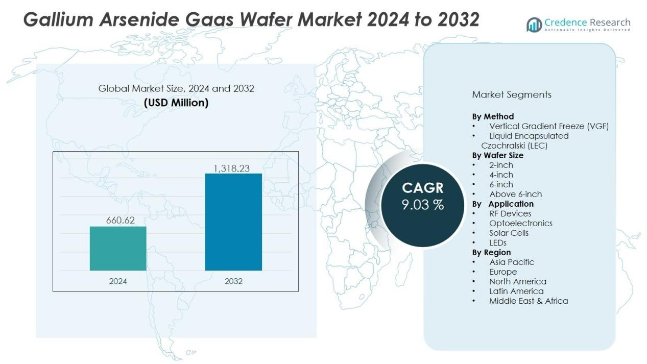
The Gallium Arsenide (GaAs) Wafer Market size was valued at USD 660.62 million in 2024 and is anticipated to reach USD 1,318.23 million by 2032, at a CAGR of 9.03% during the forecast period (2024-2032).
| REPORT ATTRIBUTE |
DETAILS |
| Historical Period |
2020-2023 |
| Base Year |
2024 |
| Forecast Period |
2025-2032 |
| Gallium Arsenide (GaAs) Wafer Market Size 2024 |
USD 660.62 Million |
| Gallium Arsenide (GaAs) Wafer Market, CAGR |
9.03% |
| Gallium Arsenide (GaAs) Wafer Market Size 2032 |
USD 1,318.23 Million |
Key drivers shaping this market include the growing penetration of smartphones, tablets, and 5G-enabled devices that require GaAs-based power amplifiers. Expanding demand for high-speed data transmission, coupled with increasing adoption of GaAs wafers in radar, satellite communication, and photovoltaic systems, is fueling growth. Their advantages such as higher electron mobility, thermal stability, and superior performance over silicon further enhance their relevance in aerospace, defense, and renewable energy applications.
Regionally, Asia-Pacific dominates the gallium arsenide wafer market, supported by strong manufacturing bases in China, Japan, and South Korea. North America holds a notable share, driven by advanced R&D, defense investments, and semiconductor innovations. Europe continues to expand steadily, supported by demand in telecom infrastructure and automotive electronics. Meanwhile, emerging markets in Latin America and the Middle East & Africa are showing potential, backed by infrastructure development and growing adoption of advanced communication technologies.
Access crucial information at unmatched prices!
Request your sample report today & start making informed decisions powered by Credence Research Inc.!
Download Sample
Market Insights:
- The gallium arsenide (GaAs) wafer market was valued at USD 660.62 million in 2024 and is projected to reach USD 1,318.23 million by 2032 at a CAGR of 9.03%.
- Rising penetration of smartphones, tablets, and 5G-enabled devices continues to drive demand for GaAs-based power amplifiers.
- Expanding applications in radar, satellite communication, and aerospace systems are fueling strong adoption of GaAs wafers.
- High electron mobility, thermal stability, and superior performance over silicon enhance their use in defense and renewable energy.
- Asia-Pacific led with 48% share in 2024, supported by strong manufacturing bases in China, Japan, South Korea, and Taiwan.
- North America held 27% share, driven by advanced R&D, defense investments, and rapid expansion of 5G and IoT applications.
- Europe accounted for 18% share, supported by telecom infrastructure growth and integration in automotive electronics such as ADAS.
Market Drivers:
Rising Demand for High-Performance Electronics and Wireless Communication:
The gallium arsenide (GaAs) wafer market benefits from increasing demand for advanced consumer electronics and wireless communication systems. Smartphones, tablets, and 5G-enabled devices rely on GaAs wafers for power amplifiers and radio frequency components. It provides high electron mobility and superior frequency performance compared to traditional silicon wafers. This capability supports faster data transmission and improved efficiency in compact devices.
- For Instance, Freiberger Compound Materials is a leading producer of LEC-grown gallium arsenide (GaAs) wafers, which offer significantly higher electron mobility than silicon. This advantage is crucial for high-frequency applications, allowing GaAs-based power amplifiers to be used in 5G mobile devices, including those operating at millimeter-wave (mmWave) frequencies up to 40 GHz.
Expanding Applications in Aerospace, Defense, and Satellite Systems:
The gallium arsenide GaAs wafer market is strongly driven by aerospace, defense, and satellite communication applications. GaAs wafers offer reliability under extreme conditions and support high-frequency radar and navigation systems. Their ability to deliver stable performance under temperature stress makes them critical in military electronics and satellite payloads. Growing investments in defense modernization programs worldwide continue to boost market demand.
- For Instance, Qorvo’s advanced X-band (8–12 GHz) radar systems use a combination of Gallium Nitride (GaN) and Gallium Arsenide (GaAs) components for mission-critical defense applications.
Growing Role in Renewable Energy and Photovoltaics:
The integration of GaAs wafers in high-efficiency solar cells is expanding, particularly in concentrated photovoltaic systems. The gallium arsenide GaAs wafer market benefits from its high energy conversion efficiency, which surpasses silicon-based alternatives. It is widely adopted in space-based solar power projects due to its durability and energy performance. Increasing focus on clean energy solutions drives further opportunities for GaAs-based photovoltaic applications.
Continuous Technological Advancements and Manufacturing Expansion:
Ongoing advancements in semiconductor technology and scaling of production facilities are supporting wider adoption of GaAs wafers. The gallium arsenide GaAs wafer market is witnessing stronger R&D investments to reduce production costs and improve yields. It has gained momentum with industry collaborations between semiconductor manufacturers and end-use industries such as telecom and automotive. This trend ensures consistent innovation, helping GaAs wafers remain competitive against alternative materials.
Market Trends:
Increasing Adoption in Advanced Communication and Optoelectronic Devices:
The gallium arsenide (GaAs) wafer market is witnessing a strong trend toward adoption in next-generation communication and optoelectronic devices. It is widely used in 5G infrastructure, wireless communication modules, and high-speed data transmission systems. Manufacturers are focusing on developing smaller, more efficient wafers to support compact device designs. Rising demand for LEDs, laser diodes, and infrared applications is further expanding the scope of GaAs wafers. The material’s superior electron mobility and thermal resistance make it a preferred choice over silicon for high-frequency and high-power applications. The ongoing expansion of IoT devices and connected technologies reinforces the importance of GaAs wafers in global supply chains.
- For Instance, Qorvo’s CMD249P5 datasheet, the CMD249P5 GaAs MMIC distributed power amplifier provides an output 1 dB compression point (\(P_{1dB}\)) of +28 dBm at 10 GHz, with 12.5 dB gain and 39 dBm output third-order intercept (\(OIP3\)).
Focus on High-Efficiency Energy Solutions and Automotive Electronics:
Another key trend shaping the gallium arsenide GaAs wafer market is its growing integration into renewable energy systems and automotive electronics. It plays a central role in concentrated photovoltaic cells, where high conversion efficiency is critical for energy generation. The aerospace sector continues to adopt GaAs wafers for space-based solar panels, leveraging their durability and energy efficiency. In the automotive industry, rising demand for advanced driver-assistance systems (ADAS) and electric vehicle power modules is supporting adoption. Manufacturers are also investing in cost reduction and scalable production processes to meet increasing demand. Strategic collaborations and research partnerships are driving innovation in wafer design, ensuring sustained growth across industries.
- For instance, researchers have achieved GaAs multijunction solar cells with conversion efficiencies of up to 29% under concentrated light, widely used in aerospace and concentrated photovoltaic applications due to superior energy yield.
Market Challenges Analysis:
High Production Costs and Complex Manufacturing Processes:
The gallium arsenide (GaAs) wafer market faces challenges from high production costs and complex fabrication requirements. It demands specialized equipment, advanced processes, and stringent quality controls, which increase overall expenses. Limited raw material availability further raises procurement costs and restricts supply chain flexibility. Manufacturers often struggle to achieve economies of scale due to the expensive nature of GaAs wafer production. The need for high-purity gallium and arsenic compounds adds another layer of complexity. These factors make cost competitiveness against silicon wafers a persistent challenge.
Environmental Concerns and Competition from Alternative Materials:
The gallium arsenide GaAs wafer market is also hindered by environmental and safety concerns linked to arsenic use. It requires careful handling and disposal measures, creating compliance and sustainability issues for producers. Growing regulatory scrutiny in developed regions increases operational challenges. Strong competition from silicon carbide (SiC) and gallium nitride (GaN) materials further limits market expansion. These alternatives offer similar performance benefits with lower environmental risks. Continuous innovation is required for GaAs wafers to maintain relevance in industries shifting toward eco-friendly solutions.
Market Opportunities:
Expansion in 5G Networks, IoT, and Advanced Communication Systems:
The gallium arsenide (GaAs) wafer market holds strong opportunities in the rapid expansion of 5G networks and IoT devices. It delivers superior frequency performance, making it essential for high-speed communication modules and power amplifiers. The rising adoption of IoT-driven applications across industries creates sustained demand for GaAs-based semiconductors. Increasing investments in satellite communication, radar, and defense electronics further strengthen growth prospects. Emerging applications in optical communication and high-frequency data transfer open new avenues for manufacturers. These factors collectively establish GaAs wafers as critical enablers of next-generation connectivity.
Rising Demand in Renewable Energy and Automotive Electronics:
The gallium arsenide GaAs wafer market also benefits from growing opportunities in renewable energy and electric vehicles. It plays a central role in high-efficiency solar panels, especially for space and concentrated photovoltaic systems. Increasing global focus on clean energy adoption drives further use of GaAs wafers in advanced solar technologies. In the automotive sector, demand for ADAS, radar systems, and EV power modules supports expansion. Manufacturers exploring cost optimization and scalable production will gain a competitive edge. These opportunities highlight the material’s potential to drive innovation across multiple high-growth industries.
Market Segmentation Analysis:
By Method:
The gallium arsenide (GaAs) wafer market is segmented by Vertical Gradient Freeze (VGF) and Liquid Encapsulated Czochralski (LEC) methods. VGF dominates due to its ability to produce high-quality crystals with fewer defects. It supports applications that require superior performance in RF and optoelectronic devices. LEC maintains relevance for specific use cases but faces limitations from higher defect densities. Growing preference for VGF reflects its reliability in advanced semiconductor production.
- For instance, PAM-XIAMEN manufactures GaAs wafers using the VGF method, offering diameters including 2, 3, 4, and 6 inches, and achieving an etch pit density (EPD) below 5000/cm² for LED applications. This low defect density is suitable for high-performance optoelectronic applications such as LEDs, laser diodes (LDs), and microelectronics.
By Wafer Size:
The gallium arsenide GaAs wafer market is categorized into 2-inch, 4-inch, 6-inch, and larger wafers. It is witnessing a clear shift toward 6-inch wafers due to better cost efficiency and scalability. Larger wafers enable higher output per batch, reducing unit costs for manufacturers. The 4-inch wafers remain in demand for smaller-scale applications and legacy systems. 2-inch wafers are gradually declining as industries move to larger formats. This trend highlights the push toward high-volume production efficiency.
- For instance, Logitech systems maintain high-quality production of 4-inch GaAs wafers, delivering repeatable surface finishes critical for semiconductor devices. 2-inch wafers are gradually declining as industries move to larger formats
By Application:
The gallium arsenide GaAs wafer market serves applications in RF devices, optoelectronics, solar cells, and LEDs. It plays a critical role in smartphones, satellite communication, and high-speed data transfer systems. Optoelectronic applications, including laser diodes and photodetectors, continue to expand demand. Solar cells, especially for aerospace and concentrated photovoltaic systems, are gaining importance. LED production also contributes, driven by high efficiency and durability requirements. The wide application base secures long-term growth for GaAs wafers.
Segmentations:
By Method:
- Vertical Gradient Freeze (VGF)
- Liquid Encapsulated Czochralski (LEC)
By Wafer Size:
- 2-inch
- 4-inch
- 6-inch
- Above 6-inch
By Application:
- RF Devices
- Optoelectronics
- Solar Cells
- LEDs
By Region:
- North America
- Europe
- Germany
- France
- U.K.
- Italy
- Spain
- Rest of Europe
- Asia Pacific
- China
- Japan
- India
- South Korea
- South-east Asia
- Rest of Asia Pacific
- Latin America
- Brazil
- Argentina
- Rest of Latin America
- Middle East & Africa
- GCC Countries
- South Africa
- Rest of the Middle East and Africa
Regional Analysis:
Asia-Pacific:
Asia-Pacific held 48% market share in the gallium arsenide (GaAs) wafer market in 2024, making it the largest regional contributor. It benefits from strong semiconductor manufacturing hubs in China, Japan, South Korea, and Taiwan. The region’s leadership is supported by heavy investments in 5G infrastructure, consumer electronics, and renewable energy projects. Rising demand for smartphones and high-speed communication devices continues to strengthen growth. Government-backed programs for advanced technology adoption further enhance regional competitiveness. Asia-Pacific remains the primary production and consumption hub for GaAs wafers.
North America:
North America accounted for 27% market share in the gallium arsenide GaAs wafer market in 2024, supported by advanced R&D activities and strong defense investments. The region leads in semiconductor innovations, particularly in aerospace, defense, and satellite communication applications. It benefits from a well-established presence of global semiconductor companies and technology startups. Expanding adoption of 5G and IoT solutions further drives demand for GaAs wafers. Favorable government policies encouraging domestic semiconductor manufacturing enhance regional growth. North America continues to position itself as a hub for innovation-driven applications of GaAs wafers.
Europe:
Europe captured 18% market share in the gallium arsenide GaAs wafer market in 2024, supported by its strong automotive and telecom sectors. It has witnessed steady demand growth from high-frequency devices, optical communication, and radar systems. Expanding integration of GaAs wafers in advanced driver-assistance systems (ADAS) boosts opportunities in the automotive industry. Telecom operators in countries such as Germany, France, and the U.K. are investing in 5G rollouts, strengthening demand further. The region also benefits from regulatory support promoting clean energy and advanced semiconductor applications. Europe maintains a solid growth trajectory supported by its diversified end-use industries.
Shape Your Report to Specific Countries or Regions & Enjoy 30% Off!
Key Player Analysis:
- Hittite Microwave
- Advanced Wireless Semiconductor
- Murata Manufacturing
- Avago Technologies
- Skyworks Solutions
- Renesas Electronics
- M/A-COM Technology Solutions
- RF Micro Devices
- Qorvo
- TriQuint Semiconductor
Competitive Analysis:
The gallium arsenide (GaAs) wafer market is highly competitive, with companies focusing on innovation, cost efficiency, and application-specific advancements. Key players include Hittite Microwave, Advanced Wireless Semiconductor, Murata Manufacturing, Avago Technologies, Skyworks Solutions, Renesas Electronics, and M/A-COM Technology Solutions. It is characterized by strong investment in R&D to improve wafer quality, reduce defect rates, and expand large-scale production capabilities. Leading firms are prioritizing strategic partnerships with telecom, aerospace, and automotive sectors to secure long-term growth. The market also reflects continuous product differentiation, where players target high-performance applications such as RF devices, optoelectronics, and solar technologies. Expanding global demand for 5G networks and advanced electronics offers competitive advantages to firms that scale efficiently and innovate rapidly. The industry remains fragmented yet dynamic, with established players leveraging technology leadership and emerging firms competing through niche offerings and specialized solutions.
Recent Developments:
- In July 2025, Renesas Electronics launched three new high-voltage 650-V GaN FETs as part of its 4th generation plus (Gen IV Plus) platform, targeting AI data centers and server power supply systems.
- In August 2025, Skyworks Solutions reported fiscal Q3 2025 results with $965 million in revenue and announced ongoing optimization of their manufacturing footprint.
Report Coverage:
The research report offers an in-depth analysis based on Method, Wafer Size, Application and Region. It details leading Market players, providing an overview of their business, product offerings, investments, revenue streams, and key applications. Additionally, the report includes insights into the competitive environment, SWOT analysis, current Market trends, as well as the primary drivers and constraints. Furthermore, it discusses various factors that have driven Market expansion in recent years. The report also explores Market dynamics, regulatory scenarios, and technological advancements that are shaping the industry. It assesses the impact of external factors and global economic changes on Market growth. Lastly, it provides strategic recommendations for new entrants and established companies to navigate the complexities of the Market.
Future Outlook:
- The gallium arsenide (GaAs) wafer market will see stronger demand from 5G infrastructure and advanced wireless communication systems.
- It is expected to gain momentum from the rising adoption of IoT-enabled devices across industries.
- The market will expand with increasing integration of GaAs wafers in radar, satellite, and defense electronics.
- Growing adoption in photovoltaic applications, especially space-based solar panels, will create new opportunities.
- It will benefit from rising demand in automotive electronics, including ADAS and EV power modules.
- The industry will witness technological advancements aimed at reducing production costs and improving wafer yields.
- Sustainability-focused manufacturing processes and recycling initiatives will become a key area of development.
- The market will continue to face competitive pressure from SiC and GaN materials, driving innovation.
- Partnerships between semiconductor firms and end-use industries will accelerate product development and commercialization.
- It will remain positioned as a critical enabler for high-frequency, high-power, and energy-efficient applications worldwide.


