Market Overview:
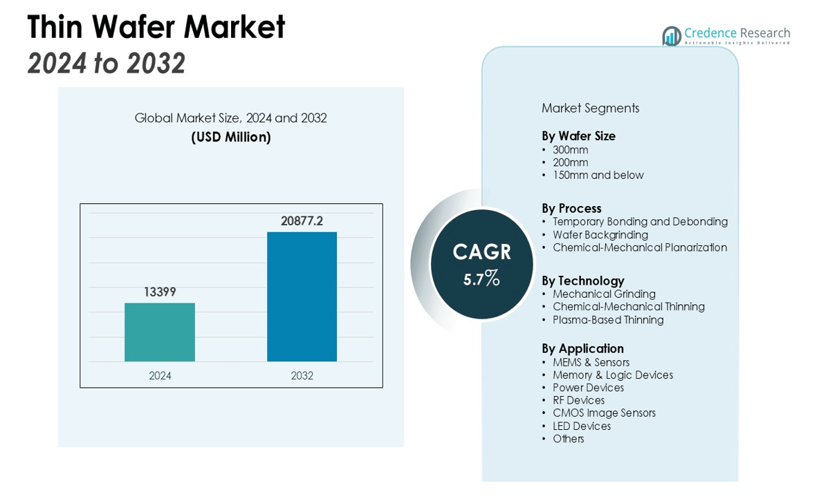
The Thin Wafer Market size was valued at USD 13399 million in 2024 and is anticipated to reach USD 20877.2 million by 2032, at a CAGR of 5.7% during the forecast period (2024-2032).
| REPORT ATTRIBUTE |
DETAILS |
| Historical Period |
2020-2023 |
| Base Year |
2024 |
| Forecast Period |
2025-2032 |
| Thin Wafer Market Size 2024 |
USD 13399 million |
| Thin Wafer Market, CAGR |
5.7% |
| Thin Wafer Market Size 2032 |
USD 20877.2 million |
Key drivers propelling the Thin Wafer Market include the rising adoption of advanced packaging technologies, growing preference for thinner and more efficient chips in mobile devices, and increasing requirements for high-density memory solutions. The surge in demand for wearable electronics and the automotive sector’s shift towards electric and autonomous vehicles further bolster market expansion. In addition, the emergence of next-generation applications such as 3D integrated circuits and advanced sensors is creating new avenues for thin wafer utilization. However, challenges related to wafer handling, breakage, and the complexities of thinning processes may restrain market growth to some extent.
Regionally, Asia Pacific leads the Thin Wafer Market, driven by strong semiconductor manufacturing capabilities in China, Taiwan, South Korea, and Japan. North America and Europe are witnessing notable growth due to technological innovations and increased investments in R&D, while emerging economies offer new opportunities for market participants.
Market Insights:
- The Thin Wafer Market reached USD 13,399 million in 2024 and is forecast to achieve USD 20,877 million by 2032, registering a CAGR of 5.7% during the forecast period.
- Advanced semiconductor packaging and integration of 3D circuits are fueling demand for ultra-thin wafers, supporting compact, high-performance devices across consumer and industrial applications.
- Miniaturization trends in smartphones, wearables, and IoT devices continue to drive manufacturers to adopt thinner and more efficient chips to meet end-user expectations.
- Automotive sector transformation, with the rise of electric and autonomous vehicles, is creating robust opportunities for thin wafer solutions in next-generation electronics and safety systems.
- Complexities in thinning, handling, and process optimization present ongoing challenges, increasing operational risks and the need for high-precision equipment and expertise.
- Asia Pacific leads with a 53% share, driven by strong manufacturing bases in China, Taiwan, South Korea, and Japan, while North America and Europe hold 21% and 16% shares, respectively, supported by innovation and strategic investments.
- Supply chain volatility, high capital investment requirements, and evolving regulatory standards remain key constraints, but growing regional diversification and R&D initiatives are broadening new opportunities for market participants.
Access crucial information at unmatched prices!
Request your sample report today & start making informed decisions powered by Credence Research Inc.!
Download Sample
Market Drivers:
Rising Adoption of Advanced Semiconductor Packaging Techniques Fuels Market Growth
The shift toward advanced semiconductor packaging technologies, such as 3D integration and system-in-package (SiP) solutions, drives robust demand in the Thin Wafer Market. These approaches require ultra-thin substrates to enable higher device density, improved performance, and enhanced energy efficiency. The need for increased chip functionality within smaller footprints pushes manufacturers to integrate thinner wafers into next-generation products. This trend supports the continued evolution of compact and high-performance electronic devices across consumer and industrial applications.
- For instance, in high-performance-computing GPUs, advanced packaging has increased the number of I/O connections to more than 10,000 per chip.
Escalating Demand for Miniaturized and High-Performance Consumer Electronics
Consumer preference for smaller, lighter, and more powerful devices strengthens the outlook for the Thin Wafer Market. It enables manufacturers to produce microprocessors, memory chips, and sensors that meet the stringent size and efficiency requirements of smartphones, tablets, and wearable devices. The continuous evolution of mobile technology, coupled with the growth of IoT ecosystems, is accelerating the use of thin wafers in mainstream applications. This dynamic encourages further research and development investments from key market participants.
- For instance, Infineon Technologies has successfully manufactured a silicon power wafer with a thickness of just 20 micrometers.
Automotive Electronics Transformation Creates New Opportunities
The automotive sector’s transition toward electric and autonomous vehicles is creating substantial opportunities for the Thin Wafer Market. Modern vehicles rely on sophisticated electronics, including ADAS, infotainment systems, and power management modules, all of which benefit from thin wafer integration. It supports increased functionality, better thermal management, and reduced system weight, aligning with the industry’s focus on safety and energy efficiency. The market is well positioned to capitalize on the growing electronic content in next-generation vehicles.
Expanding Applications in Advanced Sensors and Memory Solutions
The proliferation of advanced sensors and high-density memory solutions is a significant driver for the Thin Wafer Market. Thin wafers are integral to producing components for biometric sensors, medical devices, and industrial automation, where precision and miniaturization are critical. It also addresses the expanding need for DRAM, NAND flash, and other memory products required by data centers and high-performance computing. This broadening scope of application underlines the strategic importance of thin wafer technologies across emerging industries.
Market Trends:
Integration of Ultra-Thin Wafers into Next-Generation Semiconductor Devices Accelerates Innovation
The rapid evolution of semiconductor technology is driving the widespread adoption of ultra-thin wafers in advanced electronic devices. The Thin Wafer Market is witnessing strong momentum from the integration of thin substrates into 3D integrated circuits, flexible electronics, and advanced packaging solutions. Manufacturers are actively developing novel thinning processes and wafer handling systems to meet the increasing demand for device miniaturization without sacrificing performance or reliability. The trend toward flexible and wearable electronics, supported by advances in sensor technologies and material science, is prompting chipmakers to refine wafer thickness and enhance mechanical resilience. These innovations are also facilitating the proliferation of high-density memory solutions, critical for emerging applications in AI, IoT, and high-speed computing. Strategic partnerships between wafer suppliers and leading semiconductor companies further fuel technology advancement and accelerate time-to-market for next-generation products.
- For instance, by successfully thinning individual DRAM chips, SK hynix developed the industry’s first 12-layer HBM3 product, achieving a memory capacity of 24 gigabytes (24).
Growing Emphasis on Sustainability and Cost Optimization Shapes Manufacturing Strategies
Sustainability imperatives and the drive to lower production costs are significantly shaping the operational strategies of companies in the Thin Wafer Market. It is prompting industry stakeholders to invest in recycling initiatives, process automation, and energy-efficient manufacturing facilities to reduce material waste and environmental impact. The adoption of advanced wafer reclamation techniques and the shift toward eco-friendly production processes reflect a broader industry commitment to responsible manufacturing. This trend aligns with increasing regulatory pressures and customer expectations for greener, more sustainable electronics supply chains. The ongoing focus on cost reduction is also encouraging manufacturers to optimize wafer yield and minimize defects, ensuring consistent quality and high-volume throughput. This dual emphasis on sustainability and operational excellence is positioning the Thin Wafer Market for resilient long-term growth.
- For instance, TSMC pioneered an advanced recycling technology for waste aluminum-plastic packaging bags which, once fully adopted across its Taiwan facilities, will reduce annual incineration by 1,350 tons (1350).
Market Challenges Analysis:
Complexities in Wafer Thinning and Handling Processes Increase Production Risk
The intricate processes required to achieve ultra-thin wafer dimensions present significant challenges in the Thin Wafer Market. Manufacturers must address issues such as wafer breakage, warpage, and surface defects during thinning, dicing, and transport stages. It demands precise control of equipment and advanced handling techniques to maintain structural integrity and yield. Even minor deviations in process parameters can impact product quality and reliability. The high cost of specialized equipment and frequent need for process optimization add to operational complexity. These factors collectively raise barriers for new entrants and elevate production risk for established suppliers.
Supply Chain Volatility and High Capital Investment Limit Market Expansion
Fluctuations in raw material prices and periodic disruptions in semiconductor supply chains create persistent uncertainties for the Thin Wafer Market. It requires companies to secure stable sources for high-purity silicon and maintain strategic inventories to avoid production delays. The need for large-scale investments in R&D and manufacturing infrastructure further strains profitability, especially for smaller players. Regulatory compliance and evolving environmental standards impose additional cost burdens. This volatile landscape makes sustained market growth highly dependent on both financial resilience and adaptive supply chain management.
Market Opportunities:
Expanding Applications in Advanced Electronics and Emerging Technologies Drive New Opportunities
The increasing use of thin wafers in advanced electronic devices and next-generation technologies is creating significant growth prospects for the Thin Wafer Market. It is positioned to benefit from rising demand in fields such as 5G communications, AI-driven computing, and quantum technology. Rapid adoption of flexible and wearable devices, combined with the growing role of advanced sensors in healthcare and industrial automation, broadens the application scope for thin wafer solutions. These trends provide manufacturers with opportunities to introduce new product variants tailored to specific end-user requirements. Companies that invest in R&D to enhance wafer performance and durability are likely to capture emerging market segments.
Strategic Partnerships and Regional Expansion Accelerate Market Penetration
Collaborations between wafer suppliers, semiconductor manufacturers, and research institutes are accelerating innovation and opening new commercial avenues in the Thin Wafer Market. It benefits from increased joint ventures, technology licensing, and cross-border investments, which foster knowledge sharing and enable access to advanced fabrication capabilities. Growing focus on regional expansion, particularly in Asia Pacific and emerging economies, offers companies the chance to tap into high-growth markets with strong electronics manufacturing bases. Tailored strategies that address local regulatory requirements and customer needs further strengthen competitive positioning. This dynamic landscape enables market players to diversify revenue streams and establish long-term industry leadership.
Market Segmentation Analysis:
By Wafer Size
The 300mm wafer size segment leads the Thin Wafer Market, reflecting its dominance in advanced semiconductor manufacturing and large-scale production environments. It is favored for high-volume fabrication of memory, logic, and power devices, offering enhanced yield and cost efficiency. The 200mm wafer segment retains importance for legacy applications and specialized products, where established processes and lower costs drive continued demand. Other wafer sizes, including 150mm and below, serve niche markets with lower-volume needs and legacy equipment constraints.
- For instance, Renesas demonstrated its commitment to this wafer size by investing 90 billion yen to reopen its Kofu factory in Japan as a dedicated 300mm fab for power semiconductors.
By Process
Temporary bonding and debonding is the primary process segment, enabling manufacturers to achieve ultra-thin wafer profiles while protecting substrates from breakage or damage. This process is essential for high-precision applications, particularly in 3D integration and advanced packaging. Wafer backgrinding remains critical for thinning applications in consumer electronics and memory products, providing a balance between efficiency and reliability. Chemical-mechanical planarization supports further thinning and surface integrity, especially in demanding semiconductor processes.
- For instance, Brewer Science’s temporary bonding materials enable the handling of wafers thinned down to as little as 70 micrometers for 3D packaging applications.
By Technology
The Thin Wafer Market is propelled by advancements in both conventional and innovative wafer thinning technologies. Mechanical grinding is widely used for its efficiency and cost advantages, especially in high-volume production. Advanced techniques such as chemical-mechanical and plasma-based thinning are gaining momentum due to their ability to deliver superior wafer uniformity and preserve device integrity. This mix of technologies enables the industry to address diverse requirements in miniaturization, yield optimization, and long-term reliability.
Segmentations:
By Wafer Size
- 300mm
- 200mm
- 150mm and below
By Process
- Temporary Bonding and Debonding
- Wafer Backgrinding
- Chemical-Mechanical Planarization
By Technology
- Mechanical Grinding
- Chemical-Mechanical Thinning
- Plasma-Based Thinning
By Application
- MEMS & Sensors
- Memory & Logic Devices
- Power Devices
- RF Devices
- CMOS Image Sensors
- LED Devices
- Others
By Region
- North America
- Europe
- Germany
- France
- U.K.
- Italy
- Spain
- Rest of Europe
- Asia Pacific
- China
- Japan
- India
- South Korea
- South-east Asia
- Rest of Asia Pacific
- Latin America
- Brazil
- Argentina
- Rest of Latin America
- Middle East & Africa
- GCC Countries
- South Africa
- Rest of the Middle East and Africa
Regional Analysis:
Asia Pacific Commands Market Leadership Through Advanced Manufacturing and Investment
Asia Pacific holds 53% share of the Thin Wafer Market, maintaining the largest contribution by value and volume. The region’s dominance is anchored by robust semiconductor manufacturing ecosystems in China, Taiwan, South Korea, and Japan. Large-scale investments in fabrication facilities, technology upgrades, and skilled workforce availability further strengthen its leadership. Presence of leading foundries, packaging houses, and vertically integrated electronics firms accelerates technology adoption and innovation. Government support for R&D initiatives and incentives for semiconductor production solidify Asia Pacific’s position as the primary engine of global market expansion.
North America Demonstrates Resilience With Innovation-Driven Growth
North America holds 21% share of the Thin Wafer Market, securing its position as a significant regional player. The region benefits from strong investments in research and development, combined with a well-established base of technology firms. The semiconductor industry in North America is characterized by early adoption of advanced manufacturing processes and a focus on wafer thinning, packaging, and device integration. Leading companies in the United States collaborate with research institutes and equipment suppliers to advance miniaturization and chip performance. Emphasis on high-value applications, including data centers, AI, and automotive electronics, ensures steady demand for thin wafer solutions, while regulatory support and robust intellectual property protections contribute to market stability.
Europe Focuses on Diversification and Strategic Collaborations
Europe holds 16% share of the Thin Wafer Market, with a growing presence in specialty and advanced application segments. The region’s focus on diversification and cross-industry collaboration drives strategic investments in local semiconductor manufacturing and research hubs. European companies are forming partnerships with global wafer suppliers and academic institutions to accelerate innovation, particularly in automotive, healthcare, and industrial automation applications. Stringent environmental standards and a strong emphasis on sustainability influence sourcing and production strategies. These initiatives are enhancing Europe’s competitive stance while opening opportunities in emerging electronics and specialty technology markets.
Shape Your Report to Specific Countries or Regions & Enjoy 30% Off!
Key Player Analysis:
- STMicroelectronics
- Micron Technology
- GlobalFoundries
- Samsung Electronics
- TSMC
- Wafer World
- ShinEtsu Chemical
- SUMCO Corporation
- Nanya Technology
- Intel
- SkyWater Technology
- Sanken Electric
- Texas Instruments
- Silicon Valley Microelectronics
Competitive Analysis:
The Thin Wafer Market features intense competition among established semiconductor material providers, equipment manufacturers, and technology innovators. Leading players such as SUMCO Corporation, Siltronic AG, GlobalWafers, Shin-Etsu Chemical, and SK Siltron focus on expanding production capacity and enhancing wafer quality to maintain market leadership. It sees companies investing heavily in R&D to advance thinning processes, yield optimization, and substrate performance. Strategic partnerships with device manufacturers and investments in advanced fabrication facilities strengthen competitive positioning. The market also attracts new entrants offering specialized solutions for temporary bonding, plasma thinning, and wafer handling, intensifying rivalry. Regional players in Asia Pacific benefit from proximity to major foundries and cost-effective manufacturing, further shaping the global competitive landscape. Continuous innovation, supply chain agility, and technology integration remain critical for companies seeking to secure long-term growth in the Thin Wafer Market.
Recent Developments:
- In July 2025, STMicroelectronics announced its agreement to acquire the MEMS (micro-electromechanical systems) sensor business from NXP Semiconductors.
- In February 2025, STMicroelectronics launched the PIC100, a new data center photonics chip developed with Amazon Web Services (AWS) that supports high-speed optical interconnects.
- In October 2024, STMicroelectronics and Qualcomm Technologies announced a strategic collaboration to combine Qualcomm’s wireless technologies with ST’s STM32 microcontrollers.
Market Concentration & Characteristics:
The Thin Wafer Market demonstrates moderate to high market concentration, with a handful of large multinational companies controlling significant market shares through established manufacturing networks and advanced technological capabilities. It is characterized by intensive capital investment, high entry barriers, and a strong focus on research and innovation to achieve superior wafer quality and production efficiency. Industry participants prioritize collaborations with leading semiconductor foundries and device manufacturers to ensure consistent demand and technological advancement. The market exhibits rapid adoption of next-generation wafer thinning processes and ongoing efforts to address challenges in wafer handling, yield, and miniaturization. Competitive differentiation relies on quality, process reliability, and the ability to deliver customized solutions for diverse electronic applications.
Report Coverage:
The research report offers an in-depth analysis based on Wafers Size, Process, Technology, Application and Region. It details leading market players, providing an overview of their business, product offerings, investments, revenue streams, and key applications. Additionally, the report includes insights into the competitive environment, SWOT analysis, current market trends, as well as the primary drivers and constraints. Furthermore, it discusses various factors that have driven market expansion in recent years. The report also explores market dynamics, regulatory scenarios, and technological advancements that are shaping the industry. It assesses the impact of external factors and global economic changes on market growth. Lastly, it provides strategic recommendations for new entrants and established companies to navigate the complexities of the market.
Future Outlook:
- The Thin Wafer Market will experience strong demand from advanced packaging, 3D integration, and miniaturized electronic devices.
- Adoption of thin wafers in emerging applications such as AI, IoT, and 5G communications will accelerate.
- Automotive electronics, particularly in electric and autonomous vehicles, will present substantial growth opportunities for thin wafer suppliers.
- Advanced wafer thinning and handling technologies will become more prevalent, improving yield and process reliability.
- Companies will expand regional manufacturing bases in Asia Pacific to capitalize on established supply chains and skilled labor pools.
- Increased investments in R&D will drive innovations in wafer thickness uniformity, defect control, and substrate resilience.
- The growing use of advanced sensors and high-density memory products will further expand thin wafer utilization.
- Strategic partnerships and collaborations across the semiconductor value chain will enhance technology transfer and shorten development cycles.
- The industry will face ongoing challenges in managing production costs, supply chain volatility, and regulatory compliance.
- Sustainability initiatives and eco-friendly manufacturing practices will gain importance, shaping long-term strategies in the Thin Wafer Market.