Market Overview:
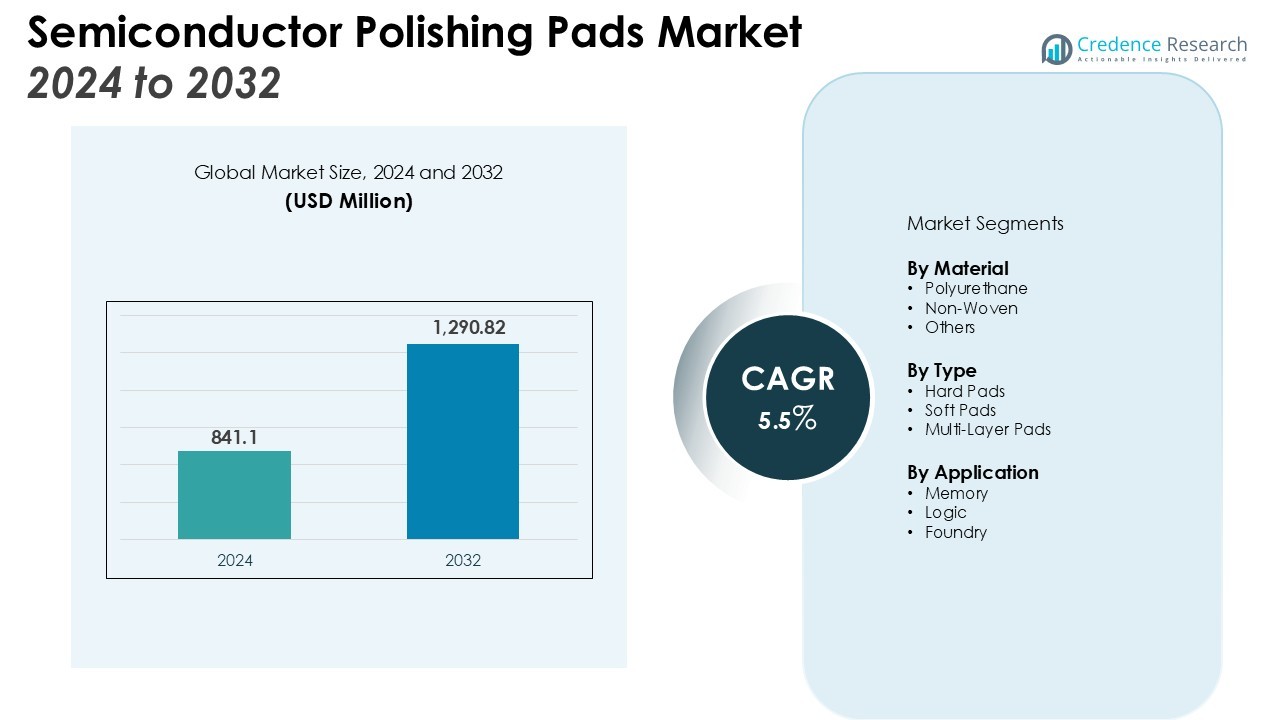
The Semiconductor Polishing Pads Market size was valued at USD 841.1 million in 2024 and is anticipated to reach USD 1,290.82 million by 2032, at a CAGR of 5.5% during the forecast period (2024-2032).
| REPORT ATTRIBUTE |
DETAILS |
| Historical Period |
2020-2023 |
| Base Year |
2024 |
| Forecast Period |
2025-2032 |
| Semiconductor Polishing Pads Market Size 2024 |
USD 841.1 Million |
| Semiconductor Polishing Pads Market, CAGR |
5.5% |
| Semiconductor Polishing Pads Market Size 2032 |
USD 1,290.82 Million |
The semiconductor polishing pads market is witnessing steady growth supported by several key factors. Demand is increasing with the development of advanced semiconductor nodes such as 5 nm and 3 nm, which require highly precise polishing processes. Expanding adoption of consumer electronics, automotive electronics, AI, IoT, and 5G infrastructure further stimulates market growth. The rising need for miniaturization and high-precision components also supports expansion, while continuous innovation in pad materials—focusing on durability, efficiency, and eco-friendly properties—drives performance improvements and wider adoption.
Asia-Pacific dominates the market, led by strong semiconductor manufacturing bases in countries including China, India, South Korea, Japan, and Taiwan. The region benefits from heavy investment in electronics production and advanced fabrication facilities. North America and Europe maintain moderate but consistent growth, supported by a strong focus on high-end applications in industries such as automotive, healthcare, and industrial electronics. Europe’s expansion is further reinforced by increasing demand for semiconductor technologies in advanced automotive systems and industrial automation. This regional structure highlights Asia-Pacific as the core hub for global production, while North America and Europe sustain growth through innovation and demand from advanced applications.
Access crucial information at unmatched prices!
Request your sample report today & start making informed decisions powered by Credence Research Inc.!
Download Sample
Market Insights:
- The Semiconductor Polishing Pads Market was valued at USD 841.1 million and is projected to reach USD 1,290.82 million by 2032, growing at a CAGR of 5.5%.
- Demand is strongly supported by advanced semiconductor nodes such as 5 nm and 3 nm that require precise wafer planarization.
- Expanding applications in consumer electronics, automotive electronics, AI, IoT, and 5G infrastructure continue to drive adoption of automated polishing systems.
- Miniaturization across automotive, healthcare, and industrial electronics reinforces the need for flawless and highly accurate polishing processes.
- Innovation in durable and eco-friendly pad materials enhances operational efficiency, reduces waste, and strengthens sustainable manufacturing practices.
- Asia-Pacific holds 61% share, positioning itself as the global leader with strong semiconductor ecosystems and large-scale investments.
- North America with 22% share and Europe with 13% share sustain steady growth, supported by advanced applications in automotive, healthcare, aerospace, and industrial sectors.
Market Drivers:
Rising Demand for Advanced Semiconductor Nodes
The Semiconductor Polishing Pads Automation Market benefits from the rapid adoption of advanced semiconductor nodes such as 5 nm and 3 nm. These smaller geometries demand extreme precision in wafer planarization, making automated polishing pad systems critical for consistent output. It supports uniformity and minimizes surface defects, ensuring high-performance chips meet industry requirements. This driver remains strong as global chipmakers pursue higher transistor density and improved efficiency.
Expanding Role of Consumer Electronics and 5G Infrastructure
The market gains momentum from surging demand in smartphones, wearables, and smart devices. Integration of 5G connectivity and AI-based features requires advanced semiconductors with flawless finishes. Automated polishing pad systems help manufacturers scale production and maintain quality standards under tight timelines. The Semiconductor Polishing Pads Automation Market aligns with this growth, strengthening its role in supporting mass production for consumer electronics.
Growing Emphasis on Miniaturization and High Precision
Miniaturization trends across automotive, healthcare, and industrial electronics reinforce the need for highly accurate polishing solutions. Automation ensures repeatability, reduces manual intervention, and lowers defect rates in wafer processing. It delivers the precision necessary for next-generation applications, where even slight imperfections can disrupt performance. The Semiconductor Polishing Pads Automation Market benefits from this emphasis on flawless and efficient production.
- For instance, the Applied Materials Reflexion LK Prime CMP system features six polishing stations that provide nanometer-level precision, critical for controlling FinFET gate height and other 3D device structures.
Innovation in Eco-Friendly and Durable Materials
Innovation in pad materials supports sustainability and operational efficiency. Manufacturers introduce eco-friendly, durable, and longer-lasting polishing pads, lowering replacement frequency and reducing waste. Automation optimizes the use of these materials by ensuring consistent pressure and usage cycles. The Semiconductor Polishing Pads Automation Market strengthens its value proposition through these material advancements, addressing both performance and environmental priorities.
- For instance, the DuPont Ikonic 9000 polishing pad features an innovative groove design and a longer lifespan, which improves slurry efficiency and reduces waste for advanced semiconductor applications.
Market Trends:
Integration of Automation with Smart Manufacturing Practices
The Semiconductor Polishing Pads Automation Market is shaped by the integration of smart manufacturing and advanced process control systems. Automation tools now align with Industry 4.0 initiatives, enabling real-time monitoring, predictive maintenance, and reduced downtime. It supports manufacturers in achieving higher throughput and consistent polishing outcomes across multiple wafer sizes. The trend emphasizes data-driven insights that improve yield and enhance cost-efficiency in semiconductor fabrication plants. Automated polishing pads are also being designed to adapt to diverse material types, supporting complex chip designs. This direction reinforces the market’s role in advancing semiconductor production standards.
- For instance, at its Regensburg plant, BMW Group employs an advanced automated surface finishing process where four AI-guided robots handle up to 1,000 vehicles every workday, ensuring consistently high quality and shorter lead times.
Focus on Sustainable and High-Performance Material Innovations
The market shows a clear trend toward eco-friendly and high-performance pad materials that extend lifespan and reduce waste. It encourages manufacturers to balance sustainability with the demand for ultra-precise wafer finishes. The Semiconductor Polishing Pads Automation Market benefits from research into recyclable and durable materials, which support cleaner production practices. Automation ensures optimal pad utilization, reducing resource consumption and operational costs. The industry also observes rising collaboration between material suppliers and automation system developers to create integrated solutions. This trend positions automated polishing pads as a critical enabler of both technological progress and environmental responsibility in the semiconductor industry.
- For instance, DuPont’s Ikonic™ 9000 series of polishing pads, which won a 2025 Edison Award, features an advanced groove design that enhances slurry efficiency and offers a longer operational life due to low wear rates.
Market Challenges Analysis:
High Cost of Advanced Automation Systems
The Semiconductor Polishing Pads Automation Market faces a challenge in the high cost of advanced automation systems. The integration of smart sensors, control units, and precision hardware requires significant capital investment. It often limits adoption to large semiconductor manufacturers with strong financial resources, while smaller players struggle to justify the expense. Ongoing maintenance and training needs further increase operational costs, adding to the financial burden. This restricts wider market penetration and slows down automation adoption in emerging economies. The cost factor continues to act as a restraint despite clear efficiency benefits.
Complexity of Process Integration and Performance Consistency
Another challenge is the complexity of integrating automated polishing systems into existing semiconductor fabrication lines. It demands seamless coordination with chemical mechanical planarization processes, which involve high precision and strict quality controls. Variations in wafer materials and device architectures make consistency difficult to achieve across all production runs. Any deviation in pad performance can lead to yield loss, which significantly impacts profitability. The Semiconductor Polishing Pads Automation Market must address these integration and performance issues to gain broader acceptance. Continuous process optimization remains essential to overcome this challenge.
Market Opportunities:
Rising Investments in Semiconductor Manufacturing Capacity
The Semiconductor Polishing Pads Automation Market holds strong opportunities from rising global investments in semiconductor manufacturing. Governments and private companies are expanding fabrication facilities to meet demand for advanced chips used in AI, 5G, and automotive electronics. It creates a favorable environment for automated polishing pad adoption, as precision and scalability are critical in new fabs. Growing initiatives in Asia-Pacific, North America, and Europe to strengthen domestic chip production further support demand. Automation ensures consistency and higher yields, making it a vital component of these large-scale expansions. This investment-driven momentum is expected to create long-term growth avenues.
Emergence of Eco-Friendly and Next-Generation Polishing Solutions
Opportunities also emerge from the growing shift toward eco-friendly and high-performance polishing pads. The Semiconductor Polishing Pads Automation Market benefits from innovation in recyclable and longer-lasting pad materials, which align with global sustainability targets. It allows manufacturers to reduce operational waste and extend product lifecycle while maintaining wafer quality. Demand for next-generation electronics, including electric vehicles and smart devices, increases the need for defect-free chips. Collaboration between automation providers and material developers opens new possibilities for integrated, efficient systems. This trend positions the market to capture growth through both performance advancement and environmental responsibility.
Market Segmentation Analysis:
By Material
The Semiconductor Polishing Pads Automation Market is segmented by material into polyurethane, non-woven, and other specialized composites. Polyurethane pads dominate due to their durability, uniformity, and suitability for high-volume wafer processing. Non-woven pads are gaining traction for niche applications where flexibility and cost efficiency are critical. It reflects the growing demand for material innovation that supports both precision and longer lifecycle performance.
- For instance, DuPont’s Suba™ 800, a polyurethane-impregnated polyester felt pad, has a hardness of 83 on the Asker C scale, showcasing its suitability for stock and intermediate polishing applications.
By Type
Market segmentation by type includes hard pads, soft pads, and multi-layer pads. Hard pads remain widely used for advanced nodes where strict planarity and low defect levels are essential. Soft pads cater to processes requiring surface adaptability and reduced scratching risks. Multi-layer pads combine performance and resilience, offering manufacturers versatility for varying wafer designs. The Semiconductor Polishing Pads Automation Market leverages these types to meet diverse semiconductor fabrication needs.
By Application
Segmentation by application covers memory, logic, and foundry segments. Memory applications demand high-volume capacity and consistency, making automation vital for efficiency. Logic devices require precision and reliability, supported by advanced polishing systems to ensure yield. Foundries act as the largest application base, driven by growing outsourcing trends in semiconductor manufacturing. It underscores the importance of automated polishing pads in scaling global chip production.
- For instance, in the memory sector, Micron Technology’s 1-gamma process node LPDDR5X memory achieves data rates up to 10.7 Gbps, a significant performance advancement enabling real-time AI processing on mobile devices.
Segmentations:
- By Material
- Polyurethane
- Non-Woven
- Others
- By Type
- Hard Pads
- Soft Pads
- Multi-Layer Pads
- By Application
- Memory
- Logic
- Foundry
- By Region
- North America
- Europe
- Asia-Pacific
- Latin America
- Middle East & Africa
Regional Analysis:
Asia-Pacific as the Core Manufacturing Hub
Asia-Pacific holds 61% share of the Semiconductor Polishing Pads Automation Market, making it the clear leader. The region benefits from advanced semiconductor ecosystems in China, Japan, South Korea, Taiwan, and India. Strong government support, heavy investments in fabrication facilities, and a skilled workforce reinforce dominance. It also gains from the presence of leading foundries and demand for consumer electronics and 5G devices. Expanding supply chains and collaborations with technology providers continue to drive its growth momentum. Asia-Pacific remains the central hub of global production and innovation.
North America’s Role in Advanced Technology Adoption
North America accounts for 22% share of the Semiconductor Polishing Pads Automation Market, reflecting steady expansion. The region benefits from research and development in high-end applications such as aerospace, defense, automotive, and healthcare electronics. Strong infrastructure and established semiconductor firms continue to invest in automation for competitiveness. It also gains from government initiatives that support domestic semiconductor capacity building. These measures strengthen resilience and reduce reliance on external supply chains. The region remains a critical market for adoption of automated polishing technologies.
Europe’s Steady Growth with Industrial Integration
Europe captures 13% share of the Semiconductor Polishing Pads Automation Market, highlighting consistent growth. Automotive and industrial electronics serve as the main drivers of demand in the region. Strong uptake in electric vehicles, advanced driver-assistance systems, and industrial automation fuels adoption. It also benefits from strict regulatory standards and sustainability-focused manufacturing practices. Collaborative efforts between research institutions and manufacturers are accelerating eco-friendly automation solutions. Europe’s emphasis on high-quality production and sustainable innovation supports its long-term market strength.
Shape Your Report to Specific Countries or Regions & Enjoy 30% Off!
Key Player Analysis:
- 3M
- Anton Paar GmbH
- Cabot Microelectronics
- Crystec Technology Trading GmbH
- DuPont
- Eminess Technologies
- Kemet International Limited
- Logitech LTD
- Ebara Corporation
- Lapmaster Wolters GmbH
- Applied Materials Inc.
Competitive Analysis:
The Semiconductor Polishing Pads Automation Market features a competitive landscape shaped by established global suppliers and emerging technology-driven firms. Leading players focus on innovation in pad materials, automation systems, and integration with advanced semiconductor fabrication processes. It emphasizes precision, durability, and eco-friendly solutions to strengthen adoption across high-volume production environments. Strategic initiatives include partnerships with semiconductor manufacturers, expansion of regional presence, and continuous research to improve performance. The market is also witnessing investments in automation technologies that align with Industry 4.0 standards, offering predictive maintenance and process optimization. Competition remains strong as companies seek to balance cost efficiency with technological advancement. This environment drives ongoing product development and ensures that firms remain focused on quality and reliability to retain competitive advantage. The Semiconductor Polishing Pads Automation Market continues to evolve with sustainability, innovation, and operational efficiency at the core of competitive positioning.
Recent Developments:
- In February 2025, 3M announced a strategic initiative to launch 1,000 new products over the subsequent three years, supported by a $3.5 billion investment in research and development.
- In January 2025, Anton Paar expanded its global footprint by opening new subsidiaries in Argentina and the United Arab Emirates.
- In July 2025, Cabot Corporation, which is related to the original entity, launched a new conductive carbon additive, LITX 95F, for use in lithium-ion batteries for energy storage systems.
Report Coverage:
The research report offers an in-depth analysis based on Material, Type, Application and Region. It details leading market players, providing an overview of their business, product offerings, investments, revenue streams, and key applications. Additionally, the report includes insights into the competitive environment, SWOT analysis, current market trends, as well as the primary drivers and constraints. Furthermore, it discusses various factors that have driven market expansion in recent years. The report also explores market dynamics, regulatory scenarios, and technological advancements that are shaping the industry. It assesses the impact of external factors and global economic changes on market growth. Lastly, it provides strategic recommendations for new entrants and established companies to navigate the complexities of the market.
Future Outlook:
- The Semiconductor Polishing Pads Automation Market will expand with rising demand for advanced semiconductor nodes that require precise wafer planarization.
- It will benefit from strong growth in consumer electronics, smart devices, and 5G infrastructure driving higher chip output.
- Increasing adoption of AI-enabled and IoT-based devices will strengthen demand for automated polishing solutions.
- The market will gain from automotive electronics, electric vehicles, and healthcare technologies that rely on defect-free semiconductors.
- Innovation in eco-friendly, durable pad materials will align with global sustainability goals and improve operational efficiency.
- Automation systems will integrate more with Industry 4.0 practices, supporting real-time monitoring and predictive maintenance.
- Investment in new semiconductor fabrication plants worldwide will create sustained opportunities for automated polishing pads.
- Asia-Pacific will remain the dominant hub, supported by strong manufacturing bases and supply chain ecosystems.
- North America will focus on high-end applications and benefit from domestic semiconductor policy initiatives.
- Europe will sustain growth through demand in automotive and industrial electronics, supported by strict quality standards.


