Market Overview
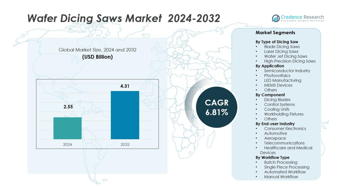
Wafer Dicing Saws Market size was valued at USD 2.55 billion in 2024 and is anticipated to reach USD 4.31 billion by 2032, growing at a CAGR of 6.81% during the forecast period.
| REPORT ATTRIBUTE |
DETAILS |
| Historical Period |
2020-2023 |
| Base Year |
2024 |
| Forecast Period |
2025-2032 |
| Wafer Dicing Saws Market Size 2024 |
USD 2.55 billion |
| Wafer Dicing Saws Market, CAGR |
6.81% |
| Wafer Dicing Saws Market Size 2032 |
USD 4.31 billion |
The Wafer Dicing Saws Market is led by DISCO Corporation, Kulicke & Soffa Industries, SPTS Technologies Ltd., Advanced Dicing Technologies (ADT), Accretech (Tokyo Seimitsu Co., Ltd.), Tokyo Seimitsu Co., Ltd., Dynatex International, Loadpoint Limited, Micro Automation, and Nippon Pulse Motor Co., Ltd. Players compete on precision, throughput, and tool uptime. Portfolios span blade, laser, and hybrid platforms with AI-driven controls. Service networks and spares availability strengthen retention. Partnerships with foundries support node transitions and ultra-thin wafer processing. Asia-Pacific is the leading region with 39% share in 2024, supported by large fabs, LED lines, and photovoltaic capacity. North America and Europe focus on advanced packaging upgrades and high-mix lines.
Market Insights
- The Wafer Dicing Saws Market was valued at USD 2.55 billion in 2024 and is projected to reach USD 4.31 billion by 2032, growing at a CAGR of 6.81%.
- Rising semiconductor production and miniaturization of electronic components drive market growth, with strong adoption in the semiconductor industry holding 54% share.
- Laser and hybrid dicing saws represent a key trend, gaining traction for precision and non-contact wafer processing across advanced packaging applications.
- The market is moderately consolidated, with major players such as DISCO Corporation and Kulicke & Soffa Industries leading through automation, AI integration, and precision upgrades.
- Asia-Pacific dominates with 39% regional share, supported by large fabs and LED manufacturing, while North America at 27% and Europe at 21% focus on high-end semiconductor production and packaging modernization.
Access crucial information at unmatched prices!
Request your sample report today & start making informed decisions powered by Credence Research Inc.!
Download Sample
Market Segmentation Analysis:
By Type of Dicing Saw
Blade dicing saws dominate the Wafer Dicing Saws Market, accounting for nearly 46% share in 2024, due to their precision cutting capability and cost efficiency across high-volume semiconductor applications. These saws are widely preferred for silicon and gallium arsenide wafer separation, offering minimal kerf loss and stable performance. Laser dicing saws are growing at a steady pace driven by the rising need for finer cuts in advanced chip packaging. Water jet and high-precision dicing saws cater to niche markets focused on brittle materials and high-value microdevices.
- For instance, DISCO Corporation employs blades with finely tuned mesh sizes and controlled feed speeds to reduce chipping in gallium arsenide, a brittle semiconductor used in RF devices.
By Application
The semiconductor industry leads the market with an estimated 54% share in 2024, supported by the expanding production of integrated circuits and miniaturized chips. Increasing demand for smartphones, automotive electronics, and IoT devices further fuels adoption. The LED manufacturing and MEMS device segments are witnessing rapid growth as wafer-level packaging and sensor production expand. Photovoltaic applications also contribute to demand, driven by growing solar cell production requiring accurate wafer separation for improved yield and efficiency.
- For instance, TSMC’s adoption of advanced wafer-level packaging for its 3-nanometer nodes has enabled higher density and performance in smartphones and data centers.
By Component
Dicing blades represent the dominant component segment, holding approximately 41% market share in 2024, owing to their critical role in achieving precise, clean cuts with minimal edge chipping. The growing preference for ultra-thin blades and advanced materials such as diamond grit supports their continued dominance. Control systems follow closely as automation and real-time process monitoring become standard in high-throughput operations. Cooling units and workholding fixtures also gain traction due to their role in maintaining temperature stability and wafer integrity during high-speed cutting operations.
Key Growth Drivers
Rising Semiconductor Production and Miniaturization
The continuous growth of the semiconductor industry drives strong demand for wafer dicing saws. Increasing production of compact and high-performance chips used in consumer electronics, automotive, and industrial devices fuels equipment adoption. Miniaturization trends demand high-precision cutting for thinner wafers and smaller dies. Manufacturers invest in advanced dicing technologies to ensure accuracy, reduce material loss, and enhance throughput. This trend supports sustained market expansion as global fabs scale up production to meet growing demand for integrated circuits and microprocessors.
- For instance, DISCO Corporation collaborated with Xanadu Quantum Technologies in 2025 to develop advanced wafer dicing and processing techniques for ultra-low loss photonic integrated chips, using their Kiru cutting and Migaku polishing technologies to enhance wafer precision and reduce optical losses.
Expansion of MEMS and LED Manufacturing
The rapid growth of MEMS sensors and LED components significantly boosts the wafer dicing saws market. Rising use of MEMS in automotive safety systems, wearables, and industrial automation increases demand for precision dicing tools. Similarly, the LED industry relies on wafer saws for accurate separation of delicate chips, enhancing yield rates. Government incentives for energy-efficient lighting accelerate LED production, particularly in Asia-Pacific. As a result, equipment manufacturers innovate saw technologies with higher precision and improved cooling systems to cater to these high-value applications.
- For instance, Bosch produces over four million MEMS sensors daily, which are used in automotive applications like airbags and brake assistance, highlighting their need for precision manufacturing processes.
Technological Advancements in Dicing Equipment
Continuous innovations in dicing technologies strengthen market performance by improving accuracy and reducing operational costs. Integration of laser-assisted cutting, AI-based monitoring, and automated control systems enhances productivity and quality consistency. These advancements minimize micro-cracks and improve wafer edge quality, crucial for next-generation semiconductor packaging. The adoption of hybrid dicing saws combining mechanical and laser techniques further expands application scope. Equipment upgrades also address the demand for processing ultra-thin and fragile wafers, supporting evolving design trends in advanced electronics and 3D packaging solutions.
Key Trends & Opportunities
Shift Toward Laser and Hybrid Dicing Technologies
A major trend shaping the market is the increasing shift toward laser and hybrid dicing saws. These systems offer superior precision and minimal material stress, ideal for thin wafers and advanced packaging designs. Laser dicing also supports non-contact processing, reducing contamination risks. Semiconductor manufacturers adopt these solutions to enhance efficiency and yield in high-density chip fabrication. This trend opens opportunities for equipment suppliers to develop scalable, energy-efficient, and AI-driven systems that align with future semiconductor process nodes.
- For instance, Laser Photonics has expanded its semiconductor product line with high-speed laser wafer dicing systems that improve throughput and reduce contamination through a non-contact method.
Rising Demand Across Emerging Economies
Expanding semiconductor fabrication and assembly operations in countries like China, South Korea, and India create significant growth opportunities. Government-backed investments in domestic chip manufacturing and renewable energy industries drive wafer dicing saw demand. The rapid development of 5G infrastructure, electric vehicles, and consumer electronics boosts wafer processing volumes. Equipment suppliers benefit by establishing regional service hubs and partnerships to cater to these high-growth markets. This trend positions Asia-Pacific as a key revenue generator in the global wafer dicing saw ecosystem.
- For instance, in South Korea, Samsung is advancing construction on multiple phases of its Pyeongtaek Campus, while SK Hynix is completing an M15X plant designed for 10nm-class DRAM with a monthly capacity of around 90,000 wafers, driven by strong AI chip demand.
Key Challenges
High Equipment and Maintenance Costs
The high initial investment and ongoing maintenance costs of wafer dicing saws pose major challenges for small and mid-scale manufacturers. Advanced laser or hybrid systems require precise calibration, cleanroom conditions, and skilled operators, adding to operational expenses. Frequent replacement of dicing blades and cooling units increases long-term costs. This limits adoption among cost-sensitive players, especially in developing regions. As semiconductor devices grow more complex, balancing affordability and performance remains a pressing issue for equipment manufacturers and end users.
Technical Limitations with Ultra-Thin Wafers
Processing ultra-thin and fragile wafers introduces challenges related to chipping, cracking, and heat-induced damage. Traditional blade dicing methods often struggle to maintain yield consistency with reduced wafer thickness. Although laser dicing provides a solution, it demands precise energy control and higher capital investment. Managing heat dissipation and maintaining alignment accuracy during high-speed cutting are critical for ensuring quality output. These technical barriers push manufacturers to explore advanced automation, real-time monitoring, and material-specific cutting methods to overcome wafer fragility constraints.
Regional Analysis
North America
North America holds 27% share of the Wafer Dicing Saws Market in 2024, driven by strong semiconductor manufacturing in the U.S. and Canada. The presence of major chip producers such as Intel, Texas Instruments, and GlobalFoundries strengthens regional equipment demand. Growth in advanced packaging, automotive electronics, and AI chip development supports steady adoption. Continuous investments in wafer fabrication plants and R&D for next-generation semiconductor materials further enhance market growth. Strategic collaborations with Asian suppliers also aid in maintaining technological competitiveness across the region.
Europe
Europe accounts for 21% market share in 2024, supported by robust semiconductor production in Germany, France, and the Netherlands. The region’s focus on automotive electronics, industrial automation, and renewable energy technologies fuels wafer dicing equipment demand. Key manufacturers like Infineon Technologies and STMicroelectronics continue to invest in automation and wafer-level packaging. The European Union’s semiconductor sovereignty initiatives and funding under the EU Chips Act strengthen equipment localization and innovation. Growing adoption of high-precision laser dicing systems reflects the region’s shift toward advanced and sustainable manufacturing.
Asia-Pacific
Asia-Pacific dominates the global market with 39% share in 2024, led by major manufacturing hubs in China, Japan, South Korea, and Taiwan. The region’s strong semiconductor ecosystem and large-scale LED and photovoltaic production underpin growth. Expanding foundry capacities from companies such as TSMC, Samsung, and SMIC drive continuous demand for high-precision dicing saws. Government incentives promoting domestic chip fabrication and renewable energy projects further accelerate adoption. Continuous advancements in AI-integrated control systems and hybrid dicing technologies reinforce Asia-Pacific’s leadership in the global supply chain.
Latin America
Latin America holds 7% market share in 2024, primarily driven by growing electronics assembly and renewable energy industries in Brazil and Mexico. Increasing adoption of photovoltaic systems and consumer electronics production supports demand for wafer processing tools. Strategic partnerships with Asian and North American equipment providers enhance regional technological capabilities. Though the semiconductor ecosystem remains nascent, rising government support for local electronics manufacturing fosters gradual market expansion. The focus on training programs and technology transfer also aids the region’s shift toward precision manufacturing capabilities.
Middle East & Africa
The Middle East & Africa represents 6% share of the Wafer Dicing Saws Market in 2024. Growth is supported by emerging investments in electronics manufacturing and renewable energy sectors, particularly in the UAE, Israel, and South Africa. Increasing solar wafer production and adoption of semiconductor equipment in research institutions enhance market prospects. Strategic collaborations with global suppliers and government-led diversification initiatives under programs like Saudi Vision 2030 stimulate technology inflow. Although market maturity remains low, rising infrastructure development and digital transformation create long-term opportunities for wafer dicing saw adoption.
Market Segmentations:
By Type of Dicing Saw
- Blade Dicing Saws
- Laser Dicing Saws
- Water Jet Dicing Saws
- High-Precision Dicing Saws
By Application
- Semiconductor Industry
- Photovoltaics
- LED Manufacturing
- MEMS Devices
- Others
By Component
- Dicing Blades
- Control Systems
- Cooling Units
- Workholding Fixtures
- Others
By End-user Industry
- Consumer Electronics
- Automotive
- Aerospace
- Telecommunications
- Healthcare and Medical Devices
By Workflow Type
- Batch Processing
- Single Piece Processing
- Automated Workflow
- Manual Workflow
By Region
- North America
- Europe
- Germany
- France
- U.K.
- Italy
- Spain
- Rest of Europe
- Asia Pacific
- China
- Japan
- India
- South Korea
- South-east Asia
- Rest of Asia Pacific
- Latin America
- Brazil
- Argentina
- Rest of Latin America
- Middle East & Africa
- GCC Countries
- South Africa
- Rest of the Middle East and Africa
Competitive Landscape
The competitive landscape of the Wafer Dicing Saws Market is defined by major players such as DISCO Corporation, Kulicke & Soffa Industries, Inc., SPTS Technologies Ltd., Micro Automation, Dynatex International, Loadpoint Limited, Nippon Pulse Motor Co., Ltd., Advanced Dicing Technologies (ADT), Accretech (Tokyo Seimitsu Co., Ltd.), and Tokyo Seimitsu Co., Ltd. These companies compete through innovations in precision cutting, automation, and hybrid dicing technologies to improve throughput and yield. DISCO Corporation leads the market with its extensive product portfolio and global service network. Kulicke & Soffa and ADT focus on integrating AI-based control systems and laser-assisted dicing to meet advanced semiconductor packaging needs. Strategic partnerships, mergers, and equipment upgrades are common as players aim to strengthen their presence in high-growth regions like Asia-Pacific. The focus on cost-effective, energy-efficient, and high-speed cutting solutions further defines the competitive strategies driving product differentiation and technological leadership across the market.
Shape Your Report to Specific Countries or Regions & Enjoy 30% Off!
Key Player Analysis
- DISCO Corporation
- Kulicke & Soffa Industries, Inc.
- SPTS Technologies Ltd.
- Micro Automation
- Dynatex International
- Loadpoint Limited
- Nippon Pulse Motor Co., Ltd.
- Advanced Dicing Technologies (ADT)
- Accretech (Tokyo Seimitsu Co., Ltd.)
- Tokyo Seimitsu Co., Ltd.
Recent Developments
- In March 2025, Tokyo Seimitsu Co., Ltd. and Asahi Diamond Industrial Co., Ltd. signed a joint-venture agreement to develop, manufacture, and sell “hub blades” used in dicing machines.
- In December 2024, DISCO Corporation launched the “DFD6370” dicing saw, optimized for package singulation and capable of handling wafers up to 330 × 330 mm in size.
- In May 2024, DISCO Corporation unveiled the KABRA® Process, a groundbreaking advancement in diamond wafer manufacturing.
- In August 2025, Xanadu and DISCO Corporation announced a collaboration to develop advanced wafer processing techniques for ultra-low-loss photonic integrated chips
Report Coverage
The research report offers an in-depth analysis based on Type of Dicing Saw, Application, Component, End User Industry, Workflow Type and Region. It details leading market players, providing an overview of their business, product offerings, investments, revenue streams, and key applications. Additionally, the report includes insights into the competitive environment, SWOT analysis, current market trends, as well as the primary drivers and constraints. Furthermore, it discusses various factors that have driven market expansion in recent years. The report also explores market dynamics, regulatory scenarios, and technological advancements that are shaping the industry. It assesses the impact of external factors and global economic changes on market growth. Lastly, it provides strategic recommendations for new entrants and established companies to navigate the complexities of the market.
Future Outlook
- The market will expand steadily with rising global semiconductor production and wafer miniaturization.
- Laser and hybrid dicing technologies will gain strong traction in advanced chip packaging.
- Asia-Pacific will maintain dominance due to large-scale fabs and LED manufacturing expansion.
- Automation and AI-driven control systems will enhance dicing precision and yield rates.
- MEMS and photovoltaic applications will create new revenue opportunities for equipment suppliers.
- Energy-efficient and low-maintenance dicing saws will attract investment from cost-sensitive manufacturers.
- Partnerships between equipment makers and foundries will accelerate product innovation cycles.
- Demand for ultra-thin wafer processing solutions will strengthen across consumer and automotive electronics.
- Europe and North America will focus on high-end equipment modernization and process upgrades.
- Continuous R&D in material science and cooling systems will shape the future of wafer dicing technology.