CHAPTER NO. 1 : INTRODUCTION 28
1.1.1. Report Description 28
Purpose of the Report 28
USP & Key Offerings 28
1.1.2. Key Benefits for Stakeholders 28
1.1.3. Target Audience 29
1.1.4. Report Scope 29
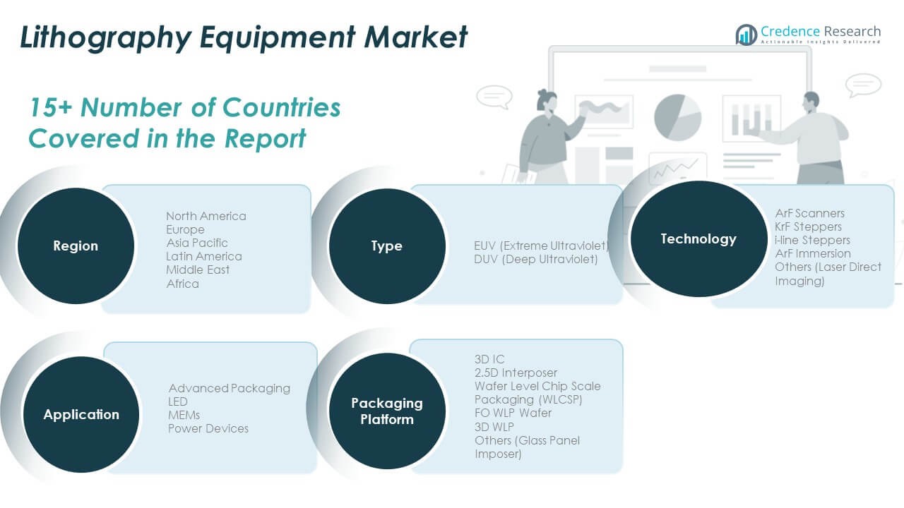
1.1.5. Regional Scope 30
CHAPTER NO. 2 : EXECUTIVE SUMMARY 31
2.1. Lithography Equipment Market Snapshot 31
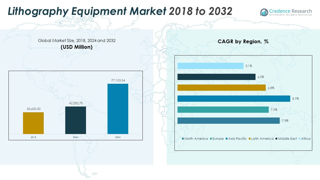
2.1.1. Global Lithography Equipment Market, 2018 – 2032 (USD Million) 32
CHAPTER NO. 3 : GEOPOLITICAL CRISIS IMPACT ANALYSIS 33
3.1. Russia-Ukraine and Israel-Palestine War Impacts 33
CHAPTER NO. 4 : LITHOGRAPHY EQUIPMENT MARKET – INDUSTRY ANALYSIS 34
4.1. Introduction 34
4.2. Market Drivers 35
4.2.1. Rising Demand for Advanced Semiconductor Nodes (≤7 nm) 35
4.2.2. Expansion of AI, IoT, and Automotive Electronics 36
4.3. Market Restraints 37
4.3.1. Extremely High Equipment Cost 37
4.4. Market Opportunities 38
4.4.1. Market Opportunity Analysis 38
4.5. Porter’s Five Forces Analysis 39
CHAPTER NO. 5 : ANALYSIS COMPETITIVE LANDSCAPE 40
5.1. Company Market Share Analysis – 2024 40
5.1.1. Global Lithography Equipment Market: Company Market Share, by Volume, 2024 40
5.1.2. Global Lithography Equipment Market: Company Market Share, by Revenue, 2024 41
5.1.3. Global Lithography Equipment Market: Top 6 Company Market Share, by Revenue, 2024 41
5.2. Global Lithography Equipment Market Company Revenue Market Share, 2024 42
5.3. Company Assessment Metrics, 2023 43
5.3.1. Stars 43
5.3.2. Emerging Leaders 43
5.3.3. Pervasive Players 43
5.3.4. Participants 43
5.4. Start-ups /SMEs Assessment Metrics, 2023 43
5.4.1. Progressive Companies 43
5.4.2. Responsive Companies 43
5.4.3. Dynamic Companies 43
5.4.4. Starting Blocks 43
5.5. Strategic Developments 44
5.5.1. Acquisitions & Mergers 44
New Product Launch 44
Regional Expansion 44
5.6. Key Players Product Matrix 45
CHAPTER NO. 6 : PESTEL & ADJACENT MARKET ANALYSIS 46
6.1. PESTEL 46
6.1.1. Political Factors 46
6.1.2. Economic Factors 46
6.1.3. Social Factors 46
6.1.4. Technological Factors 46
6.1.5. Environmental Factors 46
6.1.6. Legal Factors 46
6.2. Adjacent Market Analysis 46
CHAPTER NO. 7 : LITHOGRAPHY EQUIPMENT MARKET – BY TYPE SEGMENT ANALYSIS 47
7.1. Lithography Equipment Market Overview, by Type Segment 47
7.1.1. Lithography Equipment Market Revenue Share, By Type, 2023 & 2032 48
7.1.2. Lithography Equipment Market Attractiveness Analysis, By Type 49
7.1.3. Incremental Revenue Growth Opportunity, by Type, 2024 – 2032 49
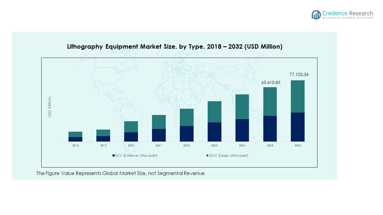
7.1.4. Lithography Equipment Market Revenue, By Type, 2018, 2023, 2027 & 2032 50
7.2. EUV (Extreme Ultraviolet) 51
7.2.1. Global EUV (Extreme Ultraviolet) Lithography Equipment Market Revenue, By Region, 2018 – 2023 (USD Million) 52
7.2.2. Global EUV (Extreme Ultraviolet) Lithography Equipment Market Revenue, By Region, 2024 – 2032 (USD Million) 52
7.3. DUV (Deep Ultraviolet) 53
7.3.1. Global DUV (Deep Ultraviolet) Lithography Equipment Market Revenue, By Region, 2018 – 2023 (USD Million) 54
7.3.2. Global DUV (Deep Ultraviolet) Lithography Equipment Market Revenue, By Region, 2024 – 2032 (USD Million) 54
CHAPTER NO. 8 : LITHOGRAPHY EQUIPMENT MARKET – BY APPLICATION SEGMENT ANALYSIS 55
8.1. Lithography Equipment Market Overview, by Application Segment 55
8.1.1. Lithography Equipment Market Revenue Share, By Application, 2023 & 2032 56
8.1.2. Lithography Equipment Market Attractiveness Analysis, By Application 57
8.1.3. Incremental Revenue Growth Opportunity, by Application, 2024 – 2032 57
8.1.4. Lithography Equipment Market Revenue, By Application, 2018, 2023, 2027 & 2032 58
8.2. Advanced Packaging 59
8.2.1. Global Advanced Packaging Lithography Equipment Market Revenue, By Region, 2018 – 2023 (USD Million) 60
8.2.2. Global Advanced Packaging Lithography Equipment Market Revenue, By Region, 2024 – 2032 (USD Million) 60
8.3. LED 61
8.3.1. Global LED Lithography Equipment Market Revenue, By Region, 2018 – 2023 (USD Million) 62
8.3.2. Global LED Lithography Equipment Market Revenue, By Region, 2024 – 2032 (USD Million) 62
8.4. MEMs 63
8.4.1. Global MEMs Lithography Equipment Market Revenue, By Region, 2018 – 2023 (USD Million) 64
8.4.2. Global MEMs Lithography Equipment Market Revenue, By Region, 2024 – 2032 (USD Million) 64
8.5. Power Devices 65
8.5.1. Global Power Devices Lithography Equipment Market Revenue, By Region, 2018 – 2023 (USD Million) 66
8.5.2. Global Power Devices Lithography Equipment Market Revenue, By Region, 2024 – 2032 (USD Million) 66
CHAPTER NO. 9 : LITHOGRAPHY EQUIPMENT MARKET – BY PACKAGING PLATFORM SEGMENT ANALYSIS 67
9.1. Lithography Equipment Market Overview, by Packaging Platform Segment 67
9.1.1. Lithography Equipment Market Revenue Share, By End-user, 2023 & 2032 68
9.1.2. Lithography Equipment Market Attractiveness Analysis, By End-user 69
9.1.3. Incremental Revenue Growth Opportunity, by End-user, 2024 – 2032 69
9.1.4. Lithography Equipment Market Revenue, By End-user, 2018, 2023, 2027 & 2032 70
9.2. 3D IC 71
9.2.1. Global 3D IC Lithography Equipment Market Revenue, By Region, 2018 – 2023 (USD Million) 72
9.2.2. Global 3D IC Lithography Equipment Market Revenue, By Region, 2024 – 2032 (USD Million) 72
9.3. 2.5D Interposer 73
9.3.1. Global 2.5D Interposer Lithography Equipment Market Revenue, By Region, 2018 – 2023 (USD Million) 74
9.3.2. Global 2.5D Interposer Lithography Equipment Market Revenue, By Region, 2024 – 2032 (USD Million) 74
9.4. Wafer Level Chip Scale Packaging (WLCSP) 75
9.4.1. Global Wafer Level Chip Scale Packaging (WLCSP) Lithography Equipment Market Revenue, By Region, 2018 – 2023 (USD Million) 76
9.4.2. Global Wafer Level Chip Scale Packaging (WLCSP) Lithography Equipment Market Revenue, By Region, 2024 – 2032 (USD Million) 76
9.5. 3D WLP 77
9.5.1. Global 3D WLP Lithography Equipment Market Revenue, By Region, 2018 – 2023 (USD Million) 78
9.5.2. Global 3D WLP Lithography Equipment Market Revenue, By Region, 2024 – 2032 (USD Million) 78
9.6. Others 79
9.6.1. Global Others Lithography Equipment Market Revenue, By Region, 2018 – 2023 (USD Million) 80
9.6.2. Global Others Lithography Equipment Market Revenue, By Region, 2024 – 2032 (USD Million) 80
CHAPTER NO. 10 : LITHOGRAPHY EQUIPMENT MARKET – BY TECHNOLOGY SEGMENT ANALYSIS 81
10.1. Lithography Equipment Market Overview, by Technology Segment 81
10.1.1. Lithography Equipment Market Revenue Share, By Technology, 2023 & 2032 82
10.1.2. Lithography Equipment Market Attractiveness Analysis, By Technology 83
10.1.3. Incremental Revenue Growth Opportunity, by Technology, 2024 – 2032 83
10.1.4. Lithography Equipment Market Revenue, By Technology, 2018, 2023, 2027 & 2032 84
10.2. ArF Scanners 85
10.2.1. Global ArF Scanners Lithography Equipment Market Revenue, By Region, 2018 – 2023 (USD Million) 86
10.2.2. Global ArF Scanners Lithography Equipment Market Revenue, By Region, 2024 – 2032 (USD Million) 86
10.3. KrF Steppers 87
10.3.1. Global KrF Steppers Lithography Equipment Market Revenue, By Region, 2018 – 2023 (USD Million) 88
10.3.2. Global KrF Steppers Lithography Equipment Market Revenue, By Region, 2024 – 2032 (USD Million) 88
10.4. i-line Steppers 89
10.4.1. Global i-line Steppers Lithography Equipment Market Revenue, By Region, 2018 – 2023 (USD Million) 90
10.4.2. Global i-line Steppers Lithography Equipment Market Revenue, By Region, 2024 – 2032 (USD Million) 90
10.5. ArF Immersion 91
10.5.1. Global ArF Immersion Lithography Equipment Market Revenue, By Region, 2018 – 2023 (USD Million) 92
10.5.2. Global ArF Immersion Lithography Equipment Market Revenue, By Region, 2024 – 2032 (USD Million) 92
10.6. Others 93
10.6.1. Global Others Lithography Equipment Market Revenue, By Region, 2018 – 2023 (USD Million) 94
10.6.2. Global Others Lithography Equipment Market Revenue, By Region, 2024 – 2032 (USD Million) 94
CHAPTER NO. 11 : LITHOGRAPHY EQUIPMENT MARKET – REGIONAL ANALYSIS 95
11.1. Lithography Equipment Market Overview, by Regional Segments 95
11.2. Region 96
11.2.1. Global Lithography Equipment Market Revenue Share, By Region, 2023 & 2032 96
11.2.2. Lithography Equipment Market Attractiveness Analysis, By Region 97
11.2.3. Incremental Revenue Growth Opportunity, by Region, 2024 – 2032 97
11.2.4. Lithography Equipment Market Revenue, By Region, 2018, 2023, 2027 & 2032 98
11.2.5. Global Lithography Equipment Market Revenue, By Region, 2018 – 2023 (USD Million) 99
11.2.6. Global Lithography Equipment Market Revenue, By Region, 2024 – 2032 (USD Million) 99
11.3. Type 100
11.3.1. Global Lithography Equipment Market Revenue, By Type, 2018 – 2023 (USD Million) 100
11.4. Global Lithography Equipment Market Revenue, By Type, 2024 – 2032 (USD Million) 100
11.5. Application 101
11.5.1. Global Lithography Equipment Market Revenue, By Application, 2018 – 2023 (USD Million) 101
11.5.2. Global Lithography Equipment Market Revenue, By Application, 2024 – 2032 (USD Million) 101
11.6. End-user 102
11.6.1. Global Lithography Equipment Market Revenue, By End-user, 2018 – 2023 (USD Million) 102
11.6.2. Global Lithography Equipment Market Revenue, By End-user, 2024 – 2032 (USD Million) 102
11.7. Technology 103
11.7.1. Global Lithography Equipment Market Revenue, By Technology, 2018 – 2023 (USD Million) 103
11.7.2. Global Lithography Equipment Market Revenue, By Technology, 2024 – 2032 (USD Million) 103
CHAPTER NO. 12 : LITHOGRAPHY EQUIPMENT MARKET – NORTH AMERICA 104
12.1. North America 104
12.1.1. Key Highlights 104
12.1.2. North America Lithography Equipment Market Revenue, By Country, 2018 – 2023 (USD Million) 105
12.1.3. North America Lithography Equipment Market Revenue, By Type, 2018 – 2023 (USD Million) 106
12.1.4. North America Lithography Equipment Market Revenue, By Application, 2018 – 2023 (USD Million) 107
12.1.5. North America Lithography Equipment Market Revenue, By End-user, 2018 – 2023 (USD Million) 108
12.1.6. North America Lithography Equipment Market Revenue, By Technology, 2018 – 2023 (USD Million) 109
12.2. U.S. 110
12.3. Canada 110
12.4. Mexico 110
CHAPTER NO. 13 : LITHOGRAPHY EQUIPMENT MARKET – EUROPE 111
13.1. Europe 111
13.1.1. Key Highlights 111
13.1.2. Europe Lithography Equipment Market Revenue, By Country, 2018 – 2023 (USD Million) 112
13.1.3. Europe Lithography Equipment Market Revenue, By Type, 2018 – 2023 (USD Million) 113
13.1.4. Europe Lithography Equipment Market Revenue, By Application, 2018 – 2023 (USD Million) 114
13.1.5. Europe Lithography Equipment Market Revenue, By End-user, 2018 – 2023 (USD Million) 115
13.1.6. Europe Lithography Equipment Market Revenue, By Technology, 2018 – 2023 (USD Million) 116
13.2. UK 117
13.3. France 117
13.4. Germany 117
13.5. Italy 117
13.6. Spain 117
13.7. Russia 117
13.8. Belgium 117
13.9. Netherland 117
13.10. Austria 117
13.11. Sweden 117
13.12. Poland 117
13.13. Denmark 117
13.14. Switzerland 117
13.15. Rest of Europe 117
CHAPTER NO. 14 : LITHOGRAPHY EQUIPMENT MARKET – ASIA PACIFIC 118
14.1. Asia Pacific 118
14.1.1. Key Highlights 118
14.1.2. Asia Pacific Lithography Equipment Market Revenue, By Country, 2018 – 2023 (USD Million) 119
14.1.3. Asia Pacific Lithography Equipment Market Revenue, By Type, 2018 – 2023 (USD Million) 120
14.1.4. Asia Pacific Lithography Equipment Market Revenue, By Application, 2018 – 2023 (USD Million) 121
14.1.5. Asia Pacific Lithography Equipment Market Revenue, By End-user, 2018 – 2023 (USD Million) 122
14.1.6. Asia Pacific Lithography Equipment Market Revenue, By Technology, 2018 – 2023 (USD Million) 123
14.2. China 124
14.3. Japan 124
14.4. South Korea 124
14.5. India 124
14.6. Australia 124
14.7. Thailand 124
14.8. Indonesia 124
14.9. Vietnam 124
14.10. Malaysia 124
14.11. Philippines 124
14.12. Taiwan 124
14.13. Rest of Asia Pacific 124
CHAPTER NO. 15 : LITHOGRAPHY EQUIPMENT MARKET – LATIN AMERICA 125
15.1. Latin America 125
15.1.1. Key Highlights 125
15.1.2. Latin America Lithography Equipment Market Revenue, By Country, 2018 – 2023 (USD Million) 126
15.1.3. Latin America Lithography Equipment Market Revenue, By Type, 2018 – 2023 (USD Million) 127
15.1.4. Latin America Lithography Equipment Market Revenue, By Application, 2018 – 2023 (USD Million) 128
15.1.5. Latin America Lithography Equipment Market Revenue, By End-user, 2018 – 2023 (USD Million) 129
15.1.6. Latin America Lithography Equipment Market Revenue, By Technology, 2018 – 2023 (USD Million) 130
15.2. Brazil 131
15.3. Argentina 131
15.4. Peru 131
15.5. Chile 131
15.6. Colombia 131
15.7. Rest of Latin America 131
CHAPTER NO. 16 : LITHOGRAPHY EQUIPMENT MARKET – MIDDLE EAST 132
16.1. Middle East 132
16.1.1. Key Highlights 132
16.1.2. Middle East Lithography Equipment Market Revenue, By Country, 2018 – 2023 (USD Million) 133
16.1.3. Middle East Lithography Equipment Market Revenue, By Type, 2018 – 2023 (USD Million) 134
16.1.4. Middle East Lithography Equipment Market Revenue, By Application, 2018 – 2023 (USD Million) 135
16.1.5. Middle East Lithography Equipment Market Revenue, By End-user, 2018 – 2023 (USD Million) 136
16.1.6. Middle East Lithography Equipment Market Revenue, By Technology, 2018 – 2023 (USD Million) 137
16.2. UAE 138
16.3. KSA 138
16.4. Israel 138
16.5. Turkey 138
16.6. Iran 138
16.7. Rest of Middle East 138
CHAPTER NO. 17 : LITHOGRAPHY EQUIPMENT MARKET – AFRICA 139
17.1. Africa 139
17.1.1. Key Highlights 139
17.1.2. Africa Lithography Equipment Market Revenue, By Country, 2018 – 2023 (USD Million) 140
17.1.3. Africa Lithography Equipment Market Revenue, By Type, 2018 – 2023 (USD Million) 141
17.1.4. Africa Lithography Equipment Market Revenue, By Application, 2018 – 2023 (USD Million) 142
17.1.5. Africa Lithography Equipment Market Revenue, By End-user, 2018 – 2023 (USD Million) 143
17.1.6. Africa Lithography Equipment Market Revenue, By Technology, 2018 – 2023 (USD Million) 144
17.2. Egypt 145
17.3. Nigeria 145
17.4. Algeria 145
17.5. Morocco 145
17.6. Rest of Africa 145
CHAPTER NO. 18 : COMPANY PROFILES 146
18.1. ASML Holding NV (Netherlands) 146
18.1.1. Company Overview 146
18.1.2. Product Portfolio 146
18.1.3. Swot Analysis 146
18.1.4. Business Strategy 147
18.1.5. Financial Overview 147
18.2. Nikon Corporation (Japan) 148
18.3. Canon, Inc. (Japan) 148
18.4. EV Group (Austria) 148
18.5. Veeco Instruments Inc. (U.S.) 148
18.6. SUSS MicroTec SE (Germany) 148
18.7. Shanghai Micro Electronics Equipment (Group) Co. Ltd. (China) 148
18.8. Neutronix Quintel Inc. (U.S.) 148
18.9. JEOL Ltd. (Japan) 148
18.10. Onto Innovation (U.S.) 148
18.11. Company 11 148
18.12. Company 12 148
18.13. Company 13 148
18.14. Company 14 148
List of Figures
FIG NO. 1. Global Lithography Equipment Market Revenue, 2018 – 2032 (USD Million) 32
FIG NO. 2. Porter’s Five Forces Analysis for Global Lithography Equipment Market 39
FIG NO. 3. Company Share Analysis, 2024 40
FIG NO. 4. Company Share Analysis, 2024 41
FIG NO. 5. Company Share Analysis, 2024 41
FIG NO. 6. Lithography Equipment Market – Company Revenue Market Share, 2024 42
FIG NO. 7. Lithography Equipment Market Revenue Share, By Type, 2023 & 2032 48
FIG NO. 8. Market Attractiveness Analysis, By Type 49
FIG NO. 9. Incremental Revenue Growth Opportunity by Type, 2024 – 2032 49
FIG NO. 10. Lithography Equipment Market Revenue, By Type, 2018, 2023, 2027 & 2032 50
FIG NO. 11. Global Lithography Equipment Market for EUV (Extreme Ultraviolet), Revenue (USD Million) 2018 – 2032 51
FIG NO. 12. Global Lithography Equipment Market for DUV (Deep Ultraviolet), Revenue (USD Million) 2018 – 2032 53
FIG NO. 13. Lithography Equipment Market Revenue Share, By Application, 2023 & 2032 56
FIG NO. 14. Market Attractiveness Analysis, By Application 57
FIG NO. 15. Incremental Revenue Growth Opportunity by Application, 2024 – 2032 57
FIG NO. 16. Lithography Equipment Market Revenue, By Application, 2018, 2023, 2027 & 2032 58
FIG NO. 17. Global Lithography Equipment Market for Advanced Packaging, Revenue (USD Million) 2018 – 2032 59
FIG NO. 18. Global Lithography Equipment Market for LED, Revenue (USD Million) 2018 – 2032 61
FIG NO. 19. Global Lithography Equipment Market for MEMs, Revenue (USD Million) 2018 – 2032 63
FIG NO. 20. Global Lithography Equipment Market for Power Devices, Revenue (USD Million) 2018 – 2032 65
FIG NO. 21. Lithography Equipment Market Revenue Share, By End-user, 2023 & 2032 68
FIG NO. 22. Market Attractiveness Analysis, By End-user 69
FIG NO. 23. Incremental Revenue Growth Opportunity by End-user, 2024 – 2032 69
FIG NO. 24. Lithography Equipment Market Revenue, By End-user, 2018, 2023, 2027 & 2032 70
FIG NO. 25. Global Lithography Equipment Market for 3D IC, Revenue (USD Million) 2018 – 2032 71
FIG NO. 26. Global Lithography Equipment Market for 2.5D Interposer, Revenue (USD Million) 2018 – 2032 73
FIG NO. 27. Global Lithography Equipment Market for Wafer Level Chip Scale Packaging (WLCSP), Revenue (USD Million) 2018 – 2032 75
FIG NO. 28. Global Lithography Equipment Market for 3D WLP, Revenue (USD Million) 2018 – 2032 77
FIG NO. 29. Global Lithography Equipment Market for Others, Revenue (USD Million) 2018 – 2032 79
FIG NO. 30. Lithography Equipment Market Revenue Share, By Technology, 2023 & 2032 82
FIG NO. 31. Market Attractiveness Analysis, By Technology 83
FIG NO. 32. Incremental Revenue Growth Opportunity by Technology, 2024 – 2032 83
FIG NO. 33. Lithography Equipment Market Revenue, By Technology, 2018, 2023, 2027 & 2032 84
FIG NO. 34. Global Lithography Equipment Market for ArF Scanners, Revenue (USD Million) 2018 – 2032 85
FIG NO. 35. Global Lithography Equipment Market for KrF Steppers, Revenue (USD Million) 2018 – 2032 87
FIG NO. 36. Global Lithography Equipment Market for i-line Steppers, Revenue (USD Million) 2018 – 2032 89
FIG NO. 37. Global Lithography Equipment Market for ArF Immersion, Revenue (USD Million) 2018 – 2032 91
FIG NO. 38. Global Lithography Equipment Market for Others, Revenue (USD Million) 2018 – 2032 93
FIG NO. 39. Global Lithography Equipment Market Revenue Share, By Region, 2023 & 2032 96
FIG NO. 40. Market Attractiveness Analysis, By Region 97
FIG NO. 41. Incremental Revenue Growth Opportunity by Region, 2024 – 2032 97
FIG NO. 42. Lithography Equipment Market Revenue, By Region, 2018, 2023, 2027 & 2032 98
FIG NO. 43. North America Lithography Equipment Market Revenue, 2018 – 2032 (USD Million) 104
FIG NO. 44. Europe Lithography Equipment Market Revenue, 2018 – 2032 (USD Million) 111
FIG NO. 45. Asia Pacific Lithography Equipment Market Revenue, 2018 – 2032 (USD Million) 118
FIG NO. 46. Latin America Lithography Equipment Market Revenue, 2018 – 2032 (USD Million) 125
FIG NO. 47. Middle East Lithography Equipment Market Revenue, 2018 – 2032 (USD Million) 132
FIG NO. 48. Africa Lithography Equipment Market Revenue, 2018 – 2032 (USD Million) 139
List of Tables
TABLE NO. 1. : Global Lithography Equipment Market: Snapshot 31
TABLE NO. 2. : Drivers for the Lithography Equipment Market: Impact Analysis 35
TABLE NO. 3. : Restraints for the Lithography Equipment Market: Impact Analysis 37
TABLE NO. 4. : Global EUV (Extreme Ultraviolet) Lithography Equipment Market Revenue, By Region, 2018 – 2023 (USD Million) 52
TABLE NO. 5. : Global EUV (Extreme Ultraviolet) Lithography Equipment Market Revenue, By Region, 2024 – 2032 (USD Million) 52
TABLE NO. 6. : Global DUV (Deep Ultraviolet) Lithography Equipment Market Revenue, By Region, 2018 – 2023 (USD Million) 54
TABLE NO. 7. : Global DUV (Deep Ultraviolet) Lithography Equipment Market Revenue, By Region, 2024 – 2032 (USD Million) 54
TABLE NO. 8. : Global Advanced Packaging Lithography Equipment Market Revenue, By Region, 2018 – 2023 (USD Million) 60
TABLE NO. 9. : Global Advanced Packaging Lithography Equipment Market Revenue, By Region, 2024 – 2032 (USD Million) 60
TABLE NO. 10. : Global LED Lithography Equipment Market Revenue, By Region, 2018 – 2023 (USD Million) 62
TABLE NO. 11. : Global LED Lithography Equipment Market Revenue, By Region, 2024 – 2032 (USD Million) 62
TABLE NO. 12. : Global MEMs Lithography Equipment Market Revenue, By Region, 2018 – 2023 (USD Million) 64
TABLE NO. 13. : Global MEMs Lithography Equipment Market Revenue, By Region, 2024 – 2032 (USD Million) 64
TABLE NO. 14. : Global Power Devices Lithography Equipment Market Revenue, By Region, 2018 – 2023 (USD Million) 66
TABLE NO. 15. : Global Power Devices Lithography Equipment Market Revenue, By Region, 2024 – 2032 (USD Million) 66
TABLE NO. 16. : Global 3D IC Lithography Equipment Market Revenue, By Region, 2018 – 2023 (USD Million) 72
TABLE NO. 17. : Global 3D IC Lithography Equipment Market Revenue, By Region, 2024 – 2032 (USD Million) 72
TABLE NO. 18. : Global 2.5D Interposer Lithography Equipment Market Revenue, By Region, 2018 – 2023 (USD Million) 74
TABLE NO. 19. : Global 2.5D Interposer Lithography Equipment Market Revenue, By Region, 2024 – 2032 (USD Million) 74
TABLE NO. 20. : Global Wafer Level Chip Scale Packaging (WLCSP) Lithography Equipment Market Revenue, By Region, 2018 – 2023 (USD Million) 76
TABLE NO. 21. : Global Wafer Level Chip Scale Packaging (WLCSP) Lithography Equipment Market Revenue, By Region, 2024 – 2032 (USD Million) 76
TABLE NO. 22. : Global 3D WLP Lithography Equipment Market Revenue, By Region, 2018 – 2023 (USD Million) 78
TABLE NO. 23. : Global 3D WLP Lithography Equipment Market Revenue, By Region, 2024 – 2032 (USD Million) 78
TABLE NO. 24. : Global Others Lithography Equipment Market Revenue, By Region, 2018 – 2023 (USD Million) 80
TABLE NO. 25. : Global Others Lithography Equipment Market Revenue, By Region, 2024 – 2032 (USD Million) 80
TABLE NO. 26. : Global ArF Scanners Lithography Equipment Market Revenue, By Region, 2018 – 2023 (USD Million) 86
TABLE NO. 27. : Global ArF Scanners Lithography Equipment Market Revenue, By Region, 2024 – 2032 (USD Million) 86
TABLE NO. 28. : Global KrF Steppers Lithography Equipment Market Revenue, By Region, 2018 – 2023 (USD Million) 88
TABLE NO. 29. : Global KrF Steppers Lithography Equipment Market Revenue, By Region, 2024 – 2032 (USD Million) 88
TABLE NO. 30. : Global i-line Steppers Lithography Equipment Market Revenue, By Region, 2018 – 2023 (USD Million) 90
TABLE NO. 31. : Global i-line Steppers Lithography Equipment Market Revenue, By Region, 2024 – 2032 (USD Million) 90
TABLE NO. 32. : Global ArF Immersion Lithography Equipment Market Revenue, By Region, 2018 – 2023 (USD Million) 92
TABLE NO. 33. : Global ArF Immersion Lithography Equipment Market Revenue, By Region, 2024 – 2032 (USD Million) 92
TABLE NO. 34. : Global Others Lithography Equipment Market Revenue, By Region, 2018 – 2023 (USD Million) 94
TABLE NO. 35. : Global Others Lithography Equipment Market Revenue, By Region, 2024 – 2032 (USD Million) 94
TABLE NO. 36. : Global Lithography Equipment Market Revenue, By Region, 2018 – 2023 (USD Million) 99
TABLE NO. 37. : Global Lithography Equipment Market Revenue, By Region, 2024 – 2032 (USD Million) 99
TABLE NO. 38. : Global Lithography Equipment Market Revenue, By Type, 2018 – 2023 (USD Million) 100
TABLE NO. 39. : Global Lithography Equipment Market Revenue, By Type, 2024 – 2032 (USD Million) 100
TABLE NO. 40. : Global Lithography Equipment Market Revenue, By Application, 2018 – 2023 (USD Million) 101
TABLE NO. 41. : Global Lithography Equipment Market Revenue, By Application, 2024 – 2032 (USD Million) 101
TABLE NO. 42. : Global Lithography Equipment Market Revenue, By End-user, 2018 – 2023 (USD Million) 102
TABLE NO. 43. : Global Lithography Equipment Market Revenue, By End-user, 2024 – 2032 (USD Million) 102
TABLE NO. 44. : Global Lithography Equipment Market Revenue, By Technology, 2018 – 2023 (USD Million) 103
TABLE NO. 45. : Global Lithography Equipment Market Revenue, By Technology, 2024 – 2032 (USD Million) 103
TABLE NO. 46. : North America Lithography Equipment Market Revenue, By Country, 2018 – 2023 (USD Million) 105
TABLE NO. 47. : North America Lithography Equipment Market Revenue, By Country, 2024 – 2032 (USD Million) 105
TABLE NO. 48. : North America Lithography Equipment Market Revenue, By Type, 2018 – 2023 (USD Million) 106
TABLE NO. 49. : North America Lithography Equipment Market Revenue, By Type, 2024 – 2032 (USD Million) 106
TABLE NO. 50. : North America Lithography Equipment Market Revenue, By Application, 2018 – 2023 (USD Million) 107
TABLE NO. 51. : North America Lithography Equipment Market Revenue, By Application, 2024 – 2032 (USD Million) 107
TABLE NO. 52. : North America Lithography Equipment Market Revenue, By End-user, 2018 – 2023 (USD Million) 108
TABLE NO. 53. : North America Lithography Equipment Market Revenue, By End-user, 2024 – 2032 (USD Million) 108
TABLE NO. 54. : North America Lithography Equipment Market Revenue, By Technology, 2018 – 2023 (USD Million) 109
TABLE NO. 55. : North America Lithography Equipment Market Revenue, By Technology, 2024 – 2032 (USD Million) 109
TABLE NO. 56. : Europe Lithography Equipment Market Revenue, By Country, 2018 – 2023 (USD Million) 112
TABLE NO. 57. : Europe Lithography Equipment Market Revenue, By Country, 2024 – 2032 (USD Million) 112
TABLE NO. 58. : Europe Lithography Equipment Market Revenue, By Type, 2018 – 2023 (USD Million) 113
TABLE NO. 59. : Europe Lithography Equipment Market Revenue, By Type, 2024 – 2032 (USD Million) 113
TABLE NO. 60. : Europe Lithography Equipment Market Revenue, By Application, 2018 – 2023 (USD Million) 114
TABLE NO. 61. : Europe Lithography Equipment Market Revenue, By Application, 2024 – 2032 (USD Million) 114
TABLE NO. 62. : Europe Lithography Equipment Market Revenue, By End-user, 2018 – 2023 (USD Million) 115
TABLE NO. 63. : Europe Lithography Equipment Market Revenue, By End-user, 2024 – 2032 (USD Million) 115
TABLE NO. 64. : Europe Lithography Equipment Market Revenue, By Technology, 2018 – 2023 (USD Million) 116
TABLE NO. 65. : Europe Lithography Equipment Market Revenue, By Technology, 2024 – 2032 (USD Million) 116
TABLE NO. 66. : Asia Pacific Lithography Equipment Market Revenue, By Country, 2018 – 2023 (USD Million) 119
TABLE NO. 67. : Asia Pacific Lithography Equipment Market Revenue, By Country, 2024 – 2032 (USD Million) 119
TABLE NO. 68. : Asia Pacific Lithography Equipment Market Revenue, By Type, 2018 – 2023 (USD Million) 120
TABLE NO. 69. : Asia Pacific Lithography Equipment Market Revenue, By Type, 2024 – 2032 (USD Million) 120
TABLE NO. 70. : Asia Pacific Lithography Equipment Market Revenue, By Application, 2018 – 2023 (USD Million) 121
TABLE NO. 71. : Asia Pacific Lithography Equipment Market Revenue, By Application, 2024 – 2032 (USD Million) 121
TABLE NO. 72. : Asia Pacific Lithography Equipment Market Revenue, By End-user, 2018 – 2023 (USD Million) 122
TABLE NO. 73. : Asia Pacific Lithography Equipment Market Revenue, By End-user, 2024 – 2032 (USD Million) 122
TABLE NO. 74. : Asia Pacific Lithography Equipment Market Revenue, By Technology, 2018 – 2023 (USD Million) 123
TABLE NO. 75. : Asia Pacific Lithography Equipment Market Revenue, By Technology, 2024 – 2032 (USD Million) 123
TABLE NO. 76. : Latin America Lithography Equipment Market Revenue, By Country, 2018 – 2023 (USD Million) 126
TABLE NO. 77. : Latin America Lithography Equipment Market Revenue, By Country, 2024 – 2032 (USD Million) 126
TABLE NO. 78. : Latin America Lithography Equipment Market Revenue, By Type, 2018 – 2023 (USD Million) 127
TABLE NO. 79. : Latin America Lithography Equipment Market Revenue, By Type, 2024 – 2032 (USD Million) 127
TABLE NO. 80. : Latin America Lithography Equipment Market Revenue, By Application, 2018 – 2023 (USD Million) 128
TABLE NO. 81. : Latin America Lithography Equipment Market Revenue, By Application, 2024 – 2032 (USD Million) 128
TABLE NO. 82. : Latin America Lithography Equipment Market Revenue, By End-user, 2018 – 2023 (USD Million) 129
TABLE NO. 83. : Latin America Lithography Equipment Market Revenue, By End-user, 2024 – 2032 (USD Million) 129
TABLE NO. 84. : Latin America Lithography Equipment Market Revenue, By Technology, 2018 – 2023 (USD Million) 130
TABLE NO. 85. : Latin America Lithography Equipment Market Revenue, By Technology, 2024 – 2032 (USD Million) 130
TABLE NO. 86. : Middle East Lithography Equipment Market Revenue, By Country, 2018 – 2023 (USD Million) 133
TABLE NO. 87. : Middle East Lithography Equipment Market Revenue, By Country, 2024 – 2032 (USD Million) 133
TABLE NO. 88. : Middle East Lithography Equipment Market Revenue, By Type, 2018 – 2023 (USD Million) 134
TABLE NO. 89. : Middle East Lithography Equipment Market Revenue, By Type, 2024 – 2032 (USD Million) 134
TABLE NO. 90. : Middle East Lithography Equipment Market Revenue, By Application, 2018 – 2023 (USD Million) 135
TABLE NO. 91. : Middle East Lithography Equipment Market Revenue, By Application, 2024 – 2032 (USD Million) 135
TABLE NO. 92. : Middle East Lithography Equipment Market Revenue, By End-user, 2018 – 2023 (USD Million) 136
TABLE NO. 93. : Middle East Lithography Equipment Market Revenue, By End-user, 2024 – 2032 (USD Million) 136
TABLE NO. 94. : Middle East Lithography Equipment Market Revenue, By Technology, 2018 – 2023 (USD Million) 137
TABLE NO. 95. : Middle East Lithography Equipment Market Revenue, By Technology, 2024 – 2032 (USD Million) 137
TABLE NO. 96. : Africa Lithography Equipment Market Revenue, By Country, 2018 – 2023 (USD Million) 140
TABLE NO. 97. : Africa Lithography Equipment Market Revenue, By Country, 2024 – 2032 (USD Million) 140
TABLE NO. 98. : Africa Lithography Equipment Market Revenue, By Type, 2018 – 2023 (USD Million) 141
TABLE NO. 99. : Africa Lithography Equipment Market Revenue, By Type, 2024 – 2032 (USD Million) 141
TABLE NO. 100. : Africa Lithography Equipment Market Revenue, By Application, 2018 – 2023 (USD Million) 142
TABLE NO. 101. : Africa Lithography Equipment Market Revenue, By Application, 2024 – 2032 (USD Million) 142
TABLE NO. 102. : Africa Lithography Equipment Market Revenue, By End-user, 2018 – 2023 (USD Million) 143
TABLE NO. 103. : Africa Lithography Equipment Market Revenue, By End-user, 2024 – 2032 (USD Million) 143
TABLE NO. 104. : Africa Lithography Equipment Market Revenue, By Technology, 2018 – 2023 (USD Million) 144
TABLE NO. 105. : Africa Lithography Equipment Market Revenue, By Technology, 2024 – 2032 (USD Million) 144