Market Overview
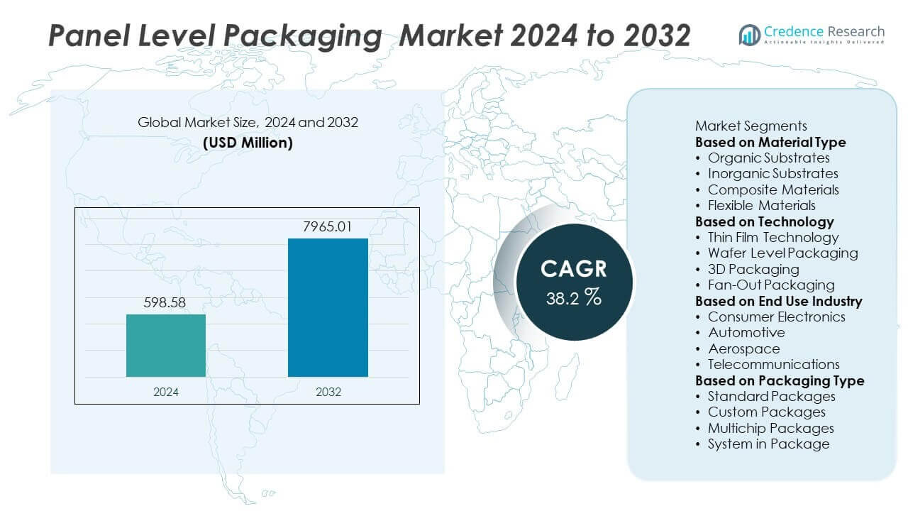
The global Panel Level Packaging (PLP) Market was valued at USD 598.58 million in 2024 and is projected to reach USD 7,965.01 million by 2032, growing at a CAGR of 38.2% during the forecast period.
| REPORT ATTRIBUTE |
DETAILS |
| Historical Period |
2020-2023 |
| Base Year |
2024 |
| Forecast Period |
2025-2032 |
| Panel Level Packaging (PLP) Market Size 2024 |
USD 598.58 Million |
| Panel Level Packaging (PLP) Market, CAGR |
38.2% |
| Panel Level Packaging (PLP) Market Size 2032 |
USD 7,965.01 Million |
The panel level packaging (PLP) market is driven by leading players such as ASE Group, Amkor Technology, JCET Group, Nepes, Deca Technologies, and Powertech Technology who dominate through capacity expansion and technological innovation. These companies focus on advancing fan-out, wafer-level, and 3D packaging solutions to support high-performance applications in consumer electronics, automotive, and 5G infrastructure. Asia Pacific led the market with over 40% share in 2024, supported by its strong semiconductor manufacturing base in China, Taiwan, South Korea, and Japan. North America held over 30% share, driven by high R&D investments and government-backed chip manufacturing initiatives.
 Market Insights
- The panel level packaging market was valued at USD 598.58 million in 2024 and is projected to reach USD 7,965.01 million by 2032, growing at a CAGR of 38.2% during the forecast period.
- Growth is driven by rising demand for high-performance consumer electronics, electric vehicles, and 5G infrastructure, requiring miniaturized, thermally efficient packaging solutions.
- Key trends include adoption of fan-out packaging with over 50% share in 2024 and rising heterogeneous integration to support AI and IoT applications.
- The market is competitive with ASE Group, Amkor Technology, JCET Group, Nepes, Deca Technologies, and Powertech Technology focusing on capacity expansion and yield improvement.
- Asia Pacific led with over 40% share, followed by North America at over 30%, supported by semiconductor manufacturing hubs. Consumer electronics accounted for over 40% of demand, with automotive emerging as a fast-growing end-use sector.
Access crucial information at unmatched prices!
Request your sample report today & start making informed decisions powered by Credence Research Inc.!
Download Sample
Market Segmentation Analysis:
By Material Type
Organic substrates dominated the panel level packaging market in 2024, capturing over 45% share. Their popularity stems from cost-effectiveness, good electrical properties, and ease of large-area panel processing. These substrates are widely used in high-density interconnects for consumer electronics and automotive components. Inorganic substrates such as glass are gaining traction for high-frequency and high-performance devices, while composite and flexible materials are emerging for lightweight and bendable applications. Growing demand for miniaturized devices and enhanced thermal performance continues to push manufacturers toward advanced organic substrate solutions.
- For instance, Henkel’s Loctite Ablestik ABP 8068TI is a pressure-less sintering die attach adhesive with an ultra-high thermal conductivity of 165 W/m-K, meeting automotive-grade reliability standards. In parallel, the company’s Loctite Eccobond UF 9000AE underfill supports large die sizes, validated on dies up to 50 mm × 50 mm, and delivers high reliability in thermal cycling tests.
By Technology
Fan-out packaging led the market with more than 50% share in 2024, driven by its ability to support high I/O counts, superior thermal dissipation, and reduced form factor. This technology is highly preferred for mobile processors, RF chips, and high-performance computing applications. Wafer-level packaging and 3D packaging are also seeing strong growth as chipmakers adopt heterogeneous integration for advanced devices. Thin-film technology remains niche but critical for ultra-thin applications. Rising demand for 5G, IoT, and AI-enabled devices is accelerating the shift toward fan-out and 3D integration technologies.
- For instance, Samsung Electro-Mechanics is developing glass substrate wafer-level packaging technology, with mass production planned for 2026. This technology offers key advantages, such as superior dimensional stability compared to organic substrates, to significantly improve signal integrity for high-performance applications like 5G and AI.
By End Use Industry
Consumer electronics accounted for the largest share, representing over 40% of the market in 2024. Demand is driven by smartphones, wearables, and tablets that require compact, high-performance packages. The automotive sector follows closely as EVs, ADAS, and infotainment systems demand advanced packaging with high reliability. Aerospace and telecommunications contribute steady growth, supported by demand for lightweight and high-frequency capable packages. The rising penetration of connected devices and growth in semiconductor content per vehicle are key factors reinforcing the dominance of consumer electronics in panel-level packaging adoption.
Key Growth Drivers
Rising Demand for High-Performance Consumer Electronics
The growing adoption of smartphones, wearables, and IoT devices is a major driver for panel level packaging (PLP). These devices require compact, lightweight, and high-performance semiconductor packages, which PLP enables through fine-pitch interconnects and high I/O density. Consumer preference for thinner devices and faster processors is pushing manufacturers to invest in PLP for greater integration efficiency. This trend supports higher production volumes and cost-effectiveness, making PLP a preferred choice for leading consumer electronics and semiconductor companies worldwide.
- For instance, in early 2025, ASE Technology Holding announced plans to establish a new fan-out panel-level packaging (FOPLP) production line capable of processing 600 mm × 600 mm substrates. ASE has historically achieved high yield rates on other packaging methods
Shift Toward Advanced Automotive Electronics
Automotive applications are fueling demand as electric vehicles (EVs), ADAS, and infotainment systems require reliable, miniaturized packaging solutions. PLP offers improved thermal management and electrical performance, essential for automotive safety and performance. The growing semiconductor content per vehicle, especially for power management and sensing, drives automakers to adopt PLP technologies. Tier-1 suppliers and semiconductor manufacturers are collaborating to integrate fan-out and 3D packaging solutions that withstand automotive-grade conditions. This shift supports growth in automotive electronics, making it one of the fastest-growing PLP end-use sectors.
- For instance, in 2024, JCET Group’s automotive electronics revenue increased significantly, driven by breakthroughs in electrified drive systems and Advanced Driver Assistance Systems (ADAS). For these and other applications, including power modules for new energy vehicles, JCET has been advancing its advanced packaging technologies to meet high-reliability and thermal management demands.
Cost Efficiency through Large-Panel Processing
PLP allows manufacturers to process multiple devices simultaneously on large panels, reducing cost per package. This scalability is a key driver as semiconductor companies seek cost-effective solutions without compromising quality. Large-panel processing improves yield and reduces material wastage compared to wafer-level packaging. As production moves toward higher volumes, PLP’s cost benefits become more significant, encouraging adoption across memory, logic, and RF device manufacturing. This cost efficiency makes PLP attractive for mass production in consumer and industrial applications, driving rapid market expansion.
Key Trends & Opportunities
Adoption of Heterogeneous Integration
The trend toward heterogeneous integration is shaping the PLP market. PLP enables combining multiple dies, memory stacks, and logic devices into a single package, improving performance and functionality. This trend is crucial for AI, 5G, and high-performance computing applications, where bandwidth and power efficiency are critical. Major players are focusing on integrating system-in-package (SiP) solutions to meet growing performance demands. The ability to integrate diverse functions in a compact footprint positions PLP as a core enabler for next-generation semiconductor innovation.
- For instance, Intel did announce significant advancements in its 2.5D chiplet and packaging technology in February 2025 at the International Solid-State Circuits Conference (ISSCC). The company demonstrated configurable, bandwidth-scalable heterogeneous 2.5D interfaces across 20 chiplets from two different foundries. The goal of this new architecture is to remove bandwidth bottlenecks in high-demand AI applications.
Expansion into 5G and High-Frequency Applications
5G infrastructure deployment is creating new opportunities for PLP adoption. PLP supports high-frequency RF devices with superior signal integrity and thermal performance. Manufacturers are investing in fan-out and glass-substrate technologies to meet the stringent requirements of 5G base stations, antennas, and devices. This expansion is expected to boost demand for advanced panel processing technologies. The growth of 5G-enabled smartphones and IoT networks further strengthens the business case for PLP, enabling high-performance connectivity solutions at competitive cost levels.
- For instance, Samsung is advancing its glass substrate technology for advanced packaging, with its Electro-Mechanics division potentially aiming for mass production by 2027. This shift to glass from conventional organic substrates is driven by the need for better dimensional stability and signal integrity for high-performance chips, including those for AI.
Key Challenges
High Initial Investment and Equipment Cost
One of the main challenges for PLP adoption is the high cost of equipment and infrastructure required for large-panel processing. Setting up panel-level manufacturing lines involves significant capital expenditure, making it challenging for smaller players to enter the market. This high barrier to entry slows adoption, especially in regions with limited semiconductor manufacturing capacity. Companies must balance cost control with the need for advanced equipment to achieve acceptable yields, which can impact profitability during the early stages of PLP deployment.
Technical Complexity and Yield Management
Achieving high yield in PLP remains a technical challenge due to warpage control, panel handling, and defect management. Larger panel sizes are more susceptible to stress and alignment issues, impacting device performance. Yield loss can significantly affect production economics, particularly in high-volume applications. Manufacturers are investing in advanced inspection and metrology tools to improve process control. However, achieving consistent quality across large panels remains a barrier, requiring continuous process optimization and collaboration between equipment vendors and semiconductor firms.
Regional Analysis
North America
North America held over 30% share of the panel level packaging market in 2024, driven by strong demand from consumer electronics, data centers, and automotive electronics. The U.S. leads the region with robust semiconductor R&D investments and early adoption of advanced packaging technologies. Growth is further supported by government incentives to boost domestic chip manufacturing. Increasing EV adoption and deployment of 5G networks are boosting demand for PLP solutions. Key players in the region are collaborating with foundries and OSATs to expand capacity and ensure supply chain resilience, strengthening North America’s competitive position in the market.
Europe
Europe accounted for around 20% market share in 2024, led by Germany, France, and the U.K. The region benefits from a strong automotive electronics base, with rising demand for ADAS, EV components, and infotainment systems driving PLP adoption. European chipmakers are investing in heterogeneous integration and fan-out technologies to support automotive safety and industrial automation requirements. The EU’s semiconductor initiatives, including the European Chips Act, are encouraging local manufacturing and reducing reliance on imports. The focus on energy efficiency and sustainability further supports growth as PLP offers reduced material usage and improved performance in next-generation devices.
Asia Pacific
Asia Pacific dominated the market with over 40% share in 2024, making it the largest regional market. China, Taiwan, South Korea, and Japan are key contributors due to their strong semiconductor manufacturing ecosystems. High consumer electronics production volumes and government support for domestic chip industries are major growth drivers. Leading OSATs and foundries are expanding PLP capacity to meet global demand. The region also benefits from cost-efficient manufacturing and access to skilled labor. The rapid expansion of 5G networks, AI-driven devices, and EV production continues to accelerate adoption of PLP across diverse applications, solidifying Asia Pacific’s leadership.
Latin America
Latin America captured around 5% market share in 2024, with growth supported by rising demand for consumer electronics and increasing automotive production in Brazil and Mexico. The region is gradually adopting advanced semiconductor packaging technologies, supported by government initiatives to attract electronics manufacturing investments. Local assembly and testing facilities are expanding to meet demand from regional markets, though dependence on imports remains high. As 5G deployment advances and industrial automation increases, PLP adoption is expected to rise, creating opportunities for global packaging players to establish partnerships and strengthen their presence in the region.
Middle East & Africa
The Middle East & Africa accounted for close to 5% share of the PLP market in 2024. Growth is primarily driven by expanding telecommunications infrastructure, with Gulf countries investing heavily in 5G networks and smart city projects. Demand from industrial automation and aerospace sectors is slowly increasing. However, limited local semiconductor manufacturing capacity restricts large-scale PLP adoption. Most demand is met through imports from Asia and Europe. Strategic collaborations and technology transfer programs are expected to improve regional capabilities, creating opportunities for future investments in local panel-level packaging facilities and supporting market growth in the coming years.
Market Segmentations:
By Material Type
- Organic Substrates
- Inorganic Substrates
- Composite Materials
- Flexible Materials
By Technology
- Thin Film Technology
- Wafer Level Packaging
- 3D Packaging
- Fan-Out Packaging
By End Use Industry
- Consumer Electronics
- Automotive
- Aerospace
- Telecommunications
By Packaging Type
- Standard Packages
- Custom Packages
- Multichip Packages
- System in Package
By Geography
- North America
- Europe
- Germany
- France
- U.K.
- Italy
- Spain
- Rest of Europe
- Asia Pacific
- China
- Japan
- India
- South Korea
- South-east Asia
- Rest of Asia Pacific
- Latin America
- Brazil
- Argentina
- Rest of Latin America
- Middle East & Africa
- GCC Countries
- South Africa
- Rest of the Middle East and Africa
Competitive Landscape
The competitive landscape of the panel level packaging (PLP) market features key players such as ASE Group, Amkor Technology, JCET Group, Nepes, Deca Technologies, and Powertech Technology leading global developments. These companies focus on expanding panel processing capacity, improving yield, and developing advanced fan-out and 3D packaging solutions. Strategic collaborations with semiconductor foundries and equipment suppliers are common as players work to optimize large-panel manufacturing. Many are investing in R&D to support heterogeneous integration and higher I/O densities required for AI, 5G, and high-performance computing applications. Partnerships with automotive and consumer electronics manufacturers are strengthening as PLP adoption grows in EVs and mobile devices. Competitive strategies include facility expansion in Asia Pacific, technology licensing, and process automation to improve cost efficiency and meet surging demand. Continuous innovation and focus on scaling production remain crucial for sustaining leadership in this fast-growing market segment.
Shape Your Report to Specific Countries or Regions & Enjoy 30% Off!
Key Player Analysis
- Greif
- Amcor
- Sonoco Products
- Pregis
- Ranpak
- International Paper
- Smurfit Kappa
- Novolex
- DS Smith
- Huhtamaki
Recent Developments
- In September 2025, Greif will be attending FACHPACK 2025 in Nuremberg from September 23-25, 2025, to showcase various sustainable industrial packaging solutions.
- In June 2025, Pregis launched a new eco-friendly panel packaging wrap made from biodegradable films with a tensile strength over 50 MPa and elongation at break around 25%.
- In May 2025, Greif received the USPS Supplier Innovation Award for its advanced recyclable panel packaging designs that enable 40% faster assembly times during logistics and shipping operations
- In 2025, Ranpak unveiled its comprehensive sustainable logistics packaging solutions at IMHX 2025, featuring the PaperWrap paper pallet wrapping system with three automation models tailored for semi-automatic to fully integrated line operations.
Report Coverage
The research report offers an in-depth analysis based on Material Type, Technology, End Use Industry, Packaging Type and Geography. It details leading market players, providing an overview of their business, product offerings, investments, revenue streams, and key applications. Additionally, the report includes insights into the competitive environment, SWOT analysis, current market trends, as well as the primary drivers and constraints. Furthermore, it discusses various factors that have driven market expansion in recent years. The report also explores market dynamics, regulatory scenarios, and technological advancements that are shaping the industry. It assesses the impact of external factors and global economic changes on market growth. Lastly, it provides strategic recommendations for new entrants and established companies to navigate the complexities of the market.
Future Outlook
- The market will see rapid adoption of fan-out and 3D packaging for high-performance devices.
- Consumer electronics will continue to drive the largest demand share for panel level packaging solutions.
- Automotive electronics growth will boost demand for reliable, thermally efficient packaging technologies.
- Large-panel processing will gain traction as manufacturers focus on cost reduction and scalability.
- Heterogeneous integration will remain a key focus to enable compact, multifunctional semiconductor packages.
- Asia Pacific will strengthen its position as the leading production hub for panel level packaging.
- North America and Europe will invest in local capacity to support supply chain resilience.
- Continuous innovation in materials will improve yield and reduce panel warpage challenges.
- Strategic collaborations between OSATs, foundries, and equipment makers will shape technology roadmaps.
- Rising demand from 5G, AI, and IoT applications will sustain double-digit growth through the forecast period.


