Table of Content
1. Preface
1.1. Report Description
1.1.1. Purpose of the Report
1.1.2. Target Audience
1.1.3. USP and Key Offerings
1.2. Research Scope
1.3. Market Introduction
2. Executive Summary
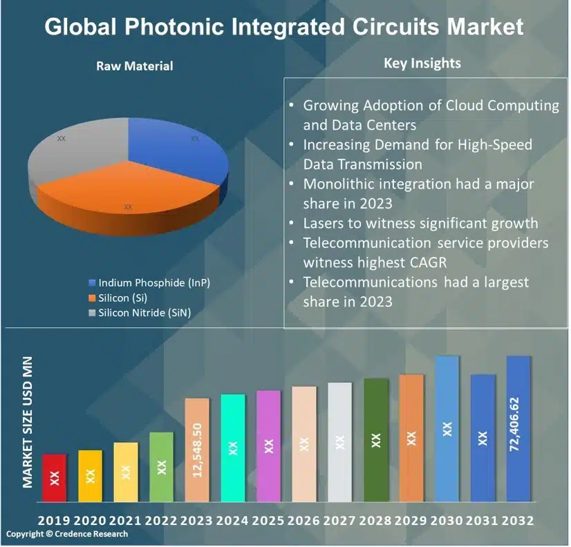
2.1. Market Snapshot: Global Photonic Integrated Circuits Market
2.1.1. Global Photonic Integrated Circuits Market, By Integration Type
2.1.2. Global Photonic Integrated Circuits Market, By Raw Material
2.1.3. Global Photonic Integrated Circuits Market, By Components
2.1.4. Global Photonic Integrated Circuits Market, By Application
2.1.5. Global Photonic Integrated Circuits Market, By End User
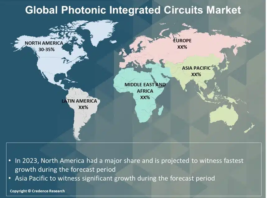
2.1.6. Global Photonic Integrated Circuits Market, By Region
2.2. Insights from Primary Respondents
3. Market Dynamics & Factors Analysis
3.1. Introduction
3.1.1. Global Photonic Integrated Circuits Market Value, 2019-2032, (US$ Mn)
3.1.2. Y-o-Y Growth Trend Analysis
3.2. Market Dynamics
3.2.1. Photonic Integrated Circuits Market Drivers
3.2.2. Photonic Integrated Circuits Market Restraints
3.2.3. Photonic Integrated Circuits Market Opportunities
3.2.4. Major Photonic Integrated Circuits Industry Challenges
3.3. Growth and Development Patterns
3.4. Investment Feasibility Analysis
3.5. Market Opportunity Analysis
3.5.1. Integration Type
3.5.2. Raw Material
3.5.3. Components
3.5.4. Application
3.5.5. End User
3.5.6. Geography
4. Market Competitive Landscape Analysis
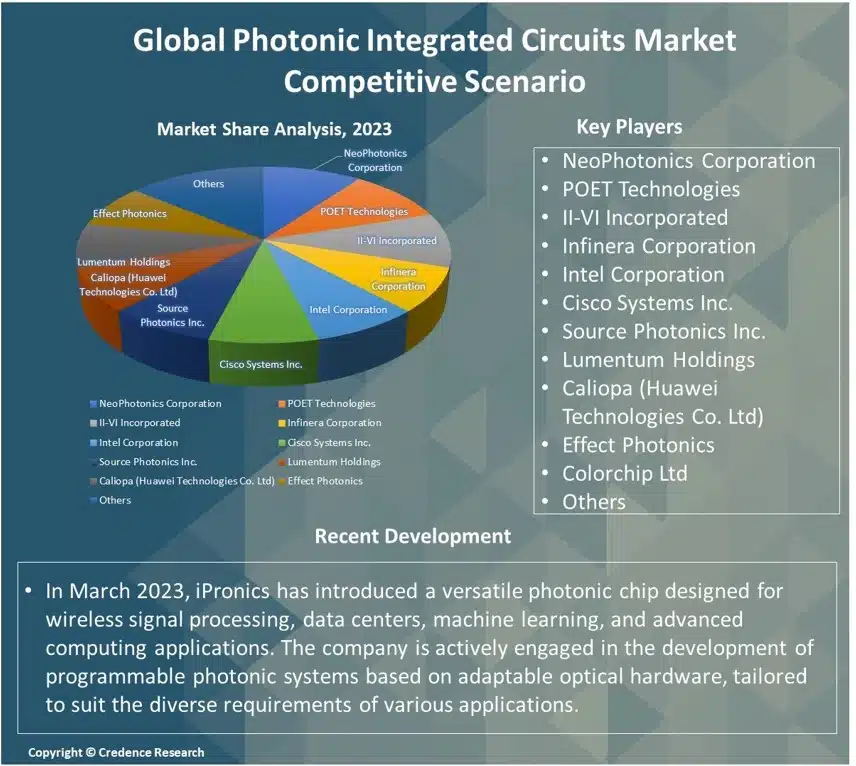
4.1. Company Market Share Analysis, 2023
4.1.1. Global Photonic Integrated Circuits Market: Company Market Share, Value 2023
4.1.2. Global Photonic Integrated Circuits Market: Top 6 Company Market Share, Value 2023
4.1.3. Global Photonic Integrated Circuits Market: Top 3 Company Market Share, Value 2023
4.2. Global Photonic Integrated Circuits Market: Company Revenue Share Analysis, 2023
4.3. Company Assessment Metrics, 2023
4.3.1. Stars
4.3.2. Emerging Leaders
4.3.3. Pervasive Players
4.3.4. Participants
4.4. Startups/ SMEs Assessment Metrics, 2023
4.4.1. Progressive Companies
4.4.2. Responsive Companies
4.4.3. Dynamic Companies
4.4.4. Starting Blocks
4.5. Strategic Development
4.5.1. Acquisition and Mergers
4.5.2. New Product Launch
4.5.3. Regional Expansion
4.5.4. Partnerships
4.6. Key Player Product Matrix
4.7. Potential for New Players in the Global Photonic Integrated Circuits Market
5. Premium Insights
5.1. STAR (Situation, Task, Action, Results) Analysis
5.2. Porter’s Five Forces Analysis
5.2.1. Threat of New Entrants
5.2.2. Bargaining Power of Buyers/Consumers
5.2.3. Bargaining Power of Suppliers
5.2.4. Threat of Substitute Types
5.2.5. Intensity of Competitive Rivalry
5.3. PESTEL Analysis
5.3.1. Political Factors
5.3.2. Economic Factors
5.3.3. Social Factors
5.3.4. Technological Factors
5.3.5. Environmental Factors
5.3.6. Legal Factors
5.4. Key Market Trends
5.4.1. Demand Side Trends
5.4.2. Supply Side Trends
5.5. Value Chain Analysis
5.6. Technology Analysis
5.6.1. Research and development in the global market
5.6.2. Patent Analysis
5.6.3. Emerging technologies and their potential disruption to the market
5.7. Consumer Behaviour Analysis
5.7.1. Consumer Preferences and Expectations
5.7.2. Factors Influencing Consumer Buying Decisions
5.7.2.1. North America
5.7.2.2. Europe
5.7.2.3. Asia Pacific
5.7.2.4. Latin America
5.7.2.5. Middle East and Africa
5.7.3. Consumer Pain Points
5.8. Analysis and Recommendations
5.9. Adjacent Market Analysis
6. Market Positioning of Key Players, 2023
6.1. Company market share of key players, 2023
6.2. Competitive Benchmarking
6.3. Market Positioning of Key Vendors
6.4. Geographical Presence Analysis
6.5. Major Strategies Adopted by Key Players
6.5.1. Key Strategies Analysis
6.5.2. Mergers and Acquisitions
6.5.3. Partnerships
6.5.4. Product Launch
6.5.5. Geographical Expansion
6.5.6. Others
7. Impact Analysis of COVID 19 and Russia – Ukraine War on Photonic Integrated Circuits Market
7.1. Ukraine-Russia War Impact
7.1.1. Uncertainty and Economic Instability
7.1.2. Supply chain disruptions
7.1.3. Regional market shifts
7.1.4. Shift in government priorities
7.2. COVID-19 Impact Analysis
7.2.1. Supply Chain Disruptions
7.2.2. Demand Fluctuations
7.2.3. Shift in Product Mix
7.2.4. Reduced Industrial Activity
7.2.5. Regional Impact Analysis
7.2.5.1. North America
7.2.5.2. Europe
7.2.5.3. Asia Pacific
7.2.5.4. Latin America
7.2.5.5. Middle East and Africa
8. Global Photonic Integrated Circuits Market, By Integration Type
8.1. Global Photonic Integrated Circuits Market Overview, by Integration Type
8.1.1. Global Photonic Integrated Circuits Market Revenue Share, By Integration Type, 2023 Vs 2032 (in %)
8.2. Monolithic Integration
8.2.1. Global Photonic Integrated Circuits Market, By Monolithic Integration, By Region, 2019-2032 (US$ Mn)
8.2.2. Market Dynamics for Monolithic Integration
8.2.2.1. Drivers
8.2.2.2. Restraints
8.2.2.3. Opportunities
8.2.2.4. Trends
8.3. Hybrid Integration
8.3.1. Global Photonic Integrated Circuits Market, By Hybrid Integration, By Region, 2019-2032 (US$ Mn)
8.3.2. Market Dynamics for Hybrid Integration
8.3.2.1. Drivers
8.3.2.2. Restraints
8.3.2.3. Opportunities
8.3.2.4. Trends
9. Global Photonic Integrated Circuits Market, By Raw Materials
9.1. Global Photonic Integrated Circuits Market Overview, by Raw Materials
9.1.1. Global Photonic Integrated Circuits Market Revenue Share, By Raw Materials, 2023 Vs 2032 (in %)
9.2. Indium Phosphide (InP)
9.2.1. Global Photonic Integrated Circuits Market, By Indium Phosphide (InP), By Region, 2019-2032 (US$ Mn)
9.2.2. Market Dynamics for Indium Phosphide (InP)
9.2.2.1. Drivers
9.2.2.2. Restraints
9.2.2.3. Opportunities
9.2.2.4. Trends
9.3. Silicon (Si)
9.3.1. Global Photonic Integrated Circuits Market, By Silicon (Si), By Region, 2019-2032 (US$ Mn)
9.3.2. Market Dynamics for Silicon (Si)
9.3.2.1. Drivers
9.3.2.2. Restraints
9.3.2.3. Opportunities
9.3.2.4. Trends
9.4. Silicon Nitride (SiN)
9.4.1. Global Photonic Integrated Circuits Market, By Silicon Nitride (SiN), By Region, 2019-2032 (US$ Mn)
9.4.2. Market Dynamics for IT and Telecom Sector
9.4.2.1. Drivers
9.4.2.2. Restraints
9.4.2.3. Opportunities
9.4.2.4. Trends
10. Global Photonic Integrated Circuits Market, By Components
10.1. Global Photonic Integrated Circuits Market Overview, by Components
10.1.1. Global Photonic Integrated Circuits Market Revenue Share, By Components, 2023 Vs 2032 (in %)
10.2. Lasers
10.2.1. Global Photonic Integrated Circuits Market, By Lasers, By Region, 2019-2032 (US$ Mn)
10.2.2. Market Dynamics for Lasers
10.2.2.1. Drivers
10.2.2.2. Restraints
10.2.2.3. Opportunities
10.2.2.4. Trends
10.3. Modulators
10.3.1. Global Photonic Integrated Circuits Market, By Modulators, By Region, 2019-2032 (US$ Mn)
10.3.2. Market Dynamics for Modulators
10.3.2.1. Drivers
10.3.2.2. Restraints
10.3.2.3. Opportunities
10.3.2.4. Trends
10.4. Detectors
10.4.1. Global Photonic Integrated Circuits Market, By Detectors, By Region, 2019-2032 (US$ Mn)
10.4.2. Market Dynamics for Detectors
10.4.2.1. Drivers
10.4.2.2. Restraints
10.4.2.3. Opportunities
10.4.2.4. Trends
10.5. Waveguides
10.5.1. Global Photonic Integrated Circuits Market, By Waveguides, By Region, 2019-2032 (US$ Mn)
10.5.2. Market Dynamics for Waveguides
10.5.2.1. Drivers
10.5.2.2. Restraints
10.5.2.3. Opportunities
10.5.2.4. Trends
10.6. Multiplexers/Demultiplexers
10.6.1. Global Photonic Integrated Circuits Market, By Multiplexers/Demultiplexers, By Region, 2019-2032 (US$ Mn)
10.6.2. Market Dynamics for Multiplexers/Demultiplexers
10.6.2.1. Drivers
10.6.2.2. Restraints
10.6.2.3. Opportunities
10.6.2.4. Trends
11. Global Photonic Integrated Circuits Market, By Application
11.1. Global Photonic Integrated Circuits Market Overview, by Application
11.1.1. Global Photonic Integrated Circuits Market Revenue Share, By Application, 2023 Vs 2032 (in %)
11.2. Telecommunications
11.2.1. Global Photonic Integrated Circuits Market, By Telecommunications, By Region, 2019-2032 (US$ Mn)
11.2.2. Market Dynamics for Telecommunications
11.2.2.1. Drivers
11.2.2.2. Restraints
11.2.2.3. Opportunities
11.2.2.4. Trends
11.3. Data Centers
11.3.1. Global Photonic Integrated Circuits Market, By Data Centers, By Region, 2019-2032 (US$ Mn)
11.3.2. Market Dynamics for Data Centers
11.3.2.1. Drivers
11.3.2.2. Restraints
11.3.2.3. Opportunities
11.3.2.4. Trends
11.4. Sensing
11.4.1. Global Photonic Integrated Circuits Market, By Sensing, By Region, 2019-2032 (US$ Mn)
11.4.2. Market Dynamics for Sensing
11.4.2.1. Drivers
11.4.2.2. Restraints
11.4.2.3. Opportunities
11.4.2.4. Trends
12. Global Photonic Integrated Circuits Market, By End User
12.1. Global Photonic Integrated Circuits Market Overview, by End User
12.1.1. Global Photonic Integrated Circuits Market Revenue Share, By End User, 2023 Vs 2032 (in %)
12.2. Telecommunication Service Providers
12.2.1. Global Photonic Integrated Circuits Market, By Telecommunication Service Providers, By Region, 2019-2032 (US$ Mn)
12.2.2. Market Dynamics for Telecommunication Service Providers
12.2.2.1. Drivers
12.2.2.2. Restraints
12.2.2.3. Opportunities
12.2.2.4. Trends
12.3. Data Center Operators
12.3.1. Global Photonic Integrated Circuits Market, By Data Center Operators, By Region, 2019-2032 (US$ Mn)
12.3.2. Market Dynamics for Data Center Operators
12.3.2.1. Drivers
12.3.2.2. Restraints
12.3.2.3. Opportunities
12.3.2.4. Trends
12.4. Healthcare
12.4.1. Global Photonic Integrated Circuits Market, By Healthcare, By Region, 2019-2032 (US$ Mn)
12.4.2. Market Dynamics for Healthcare
12.4.2.1. Drivers
12.4.2.2. Restraints
12.4.2.3. Opportunities
12.4.2.4. Trends
12.5. Defense and Aerospace
12.5.1. Global Photonic Integrated Circuits Market, By Extended – Range Cables, By Region, 2019-2032 (US$ Mn)
12.5.2. Market Dynamics for Extended – Range Cables
12.5.2.1. Drivers
12.5.2.2. Restraints
12.5.2.3. Opportunities
12.5.2.4. Trends
12.6. Manufacturing and Industrial
12.6.1. Global Photonic Integrated Circuits Market, By Manufacturing and Industrial, By Region, 2019-2032 (US$ Mn)
12.6.2. Market Dynamics for Manufacturing and Industrial
12.6.2.1. Drivers
12.6.2.2. Restraints
12.6.2.3. Opportunities
12.6.2.4. Trends
13. Global Photonic Integrated Circuits Market, By Region
13.1. Global Photonic Integrated Circuits Market Overview, by Region
13.1.1. Global Photonic Integrated Circuits Market, By Region, 2023 vs 2032 (in%)
13.2. Integration Type
13.2.1. Global Photonic Integrated Circuits Market, By Integration Type, 2019-2032 (US$ Mn)
13.3. Raw Material
13.3.1. Global Photonic Integrated Circuits Market, By Raw Material, 2019-2032 (US$ Mn)
13.4. Components
13.4.1. Global Photonic Integrated Circuits Market, By Components, 2019-2032 (US$ Mn)
13.5. Application
13.5.1. Global Photonic Integrated Circuits Market, By Application, 2019-2032 (US$ Mn)
13.6. End User
13.6.1. Global Photonic Integrated Circuits Market, By End User, 2019-2032 (US$ Mn)
14. North America Photonic Integrated Circuits Market Analysis
14.1. Overview
14.1.1. Market Dynamics for North America
14.1.1.1. Drivers
14.1.1.2. Restraints
14.1.1.3. Opportunities
14.1.1.4. Trends
14.2. North America Photonic Integrated Circuits Market, by Integration Type, 2019-2032(US$ Mn)
14.2.1. Overview
14.2.2. SRC Analysis
14.3. North America Photonic Integrated Circuits Market, by Raw Material, 2019-2032(US$ Mn)
14.3.1. Overview
14.3.2. SRC Analysis
14.4. North America Photonic Integrated Circuits Market, by Components, 2019-2032(US$ Mn)
14.4.1. Overview
14.4.2. SRC Analysis
14.5. North America Photonic Integrated Circuits Market, by Application, 2019-2032(US$ Mn)
14.5.1. Overview
14.5.2. SRC Analysis
14.6. North America Photonic Integrated Circuits Market, by End User, 2019-2032(US$ Mn)
14.6.1. Overview
14.6.2. SRC Analysis
14.7. North America Photonic Integrated Circuits Market, by Country, 2019-2032 (US$ Mn)
14.7.1. North America Photonic Integrated Circuits Market, by Country, 2023 Vs 2032 (in%)
14.7.2. U.S.
14.7.3. Canada
14.7.4. Mexico
15. Europe Photonic Integrated Circuits Market Analysis
15.1. Overview
15.1.1. Market Dynamics for North America
15.1.1.1. Drivers
15.1.1.2. Restraints
15.1.1.3. Opportunities
15.1.1.4. Trends
15.2. Europe Photonic Integrated Circuits Market, by Integration Type, 2019-2032(US$ Mn)
15.2.1. Overview
15.2.2. SRC Analysis
15.3. Europe Photonic Integrated Circuits Market, by Raw Material, 2019-2032(US$ Mn)
15.3.1. Overview
15.3.2. SRC Analysis
15.4. Europe Photonic Integrated Circuits Market, by Components, 2019-2032(US$ Mn)
15.4.1. Overview
15.4.2. SRC Analysis
15.5. Europe Photonic Integrated Circuits Market, by Application, 2019-2032(US$ Mn)
15.5.1. Overview
15.5.2. SRC Analysis
15.6. Europe Photonic Integrated Circuits Market, by End User, 2019-2032(US$ Mn)
15.6.1. Overview
15.6.2. SRC Analysis
15.7. Europe Photonic Integrated Circuits Market, by Country, 2019-2032 (US$ Mn)
15.7.1. Europe Photonic Integrated Circuits Market, by Country, 2023 Vs 2032 (in%)
15.7.2. UK
15.7.3. France
15.7.4. Germany
15.7.5. Italy
15.7.6. Spain
15.7.7. Benelux
15.7.8. Russia
15.7.9. Rest of Europe
16. Asia Pacific Photonic Integrated Circuits Market Analysis
16.1. Overview
16.1.1. Market Dynamics for North America
16.1.1.1. Drivers
16.1.1.2. Restraints
16.1.1.3. Opportunities
16.1.1.4. Trends
16.2. Asia Pacific Photonic Integrated Circuits Market, by Integration Type, 2019-2032(US$ Mn)
16.2.1. Overview
16.2.2. SRC Analysis
16.3. Asia Pacific Photonic Integrated Circuits Market, by Raw Material, 2019-2032(US$ Mn)
16.3.1. Overview
16.3.2. SRC Analysis
16.4. Asia Pacific Photonic Integrated Circuits Market, by Components, 2019-2032(US$ Mn)
16.4.1. Overview
16.4.2. SRC Analysis
16.5. Asia Pacific Photonic Integrated Circuits Market, by Application, 2019-2032(US$ Mn)
16.5.1. Overview
16.5.2. SRC Analysis
16.6. Asia Pacific Photonic Integrated Circuits Market, by End User, 2019-2032(US$ Mn)
16.6.1. Overview
16.6.2. SRC Analysis
16.7. Asia Pacific Photonic Integrated Circuits Market, by Country, 2019-2032 (US$ Mn)
16.7.1. Asia Pacific Photonic Integrated Circuits Market, by Country, 2023 Vs 2032 (in%)
16.7.2. China
16.7.3. Japan
16.7.4. India
16.7.5. South Korea
16.7.6. South East Asia
16.7.7. Rest of Asia Pacific
17. Latin America Photonic Integrated Circuits Market Analysis
17.1. Overview
17.1.1. Market Dynamics for North America
17.1.1.1. Drivers
17.1.1.2. Restraints
17.1.1.3. Opportunities
17.1.1.4. Trends
17.2. Latin America Photonic Integrated Circuits Market, by Integration Type, 2019-2032(US$ Mn)
17.2.1. Overview
17.2.2. SRC Analysis
17.3. Latin America Photonic Integrated Circuits Market, by Raw Material, 2019-2032(US$ Mn)
17.3.1. Overview
17.3.2. SRC Analysis
17.4. Latin America Photonic Integrated Circuits Market, by Components, 2019-2032(US$ Mn)
17.4.1. Overview
17.4.2. SRC Analysis
17.5. Latin America Photonic Integrated Circuits Market, by Application, 2019-2032(US$ Mn)
17.5.1. Overview
17.5.2. SRC Analysis
17.6. Latin America Photonic Integrated Circuits Market, by End User, 2019-2032(US$ Mn)
17.6.1. Overview
17.6.2. SRC Analysis
17.7. Latin America Photonic Integrated Circuits Market, by Country, 2019-2032 (US$ Mn)
17.7.1. Latin America Photonic Integrated Circuits Market, by Country, 2023 Vs 2032 (in%)
17.7.2. Brazil
17.7.3. Argentina
17.7.4. Rest of Latin America
18. Middle East Photonic Integrated Circuits Market Analysis
18.1. Overview
18.1.1. Market Dynamics for North America
18.1.1.1. Drivers
18.1.1.2. Restraints
18.1.1.3. Opportunities
18.1.1.4. Trends
18.2. Middle East Photonic Integrated Circuits Market, by Integration Type, 2019-2032(US$ Mn)
18.2.1. Overview
18.2.2. SRC Analysis
18.3. Middle East Photonic Integrated Circuits Market, by Raw Material, 2019-2032(US$ Mn)
18.3.1. Overview
18.3.2. SRC Analysis
18.4. Middle East Photonic Integrated Circuits Market, by Components, 2019-2032(US$ Mn)
18.4.1. Overview
18.4.2. SRC Analysis
18.5. Middle East Photonic Integrated Circuits Market, by Application, 2019-2032(US$ Mn)
18.5.1. Overview
18.5.2. SRC Analysis
18.6. Middle East Photonic Integrated Circuits Market, by End User, 2019-2032(US$ Mn)
18.6.1. Overview
18.6.2. SRC Analysis
18.7. Middle East Photonic Integrated Circuits Market, by Country, 2019-2032 (US$ Mn)
18.7.1. Middle East Photonic Integrated Circuits Market, by Country, 2023 Vs 2032 (in%)
18.7.2. UAE
18.7.3. Saudi Arabia
18.7.4. Rest of Middle East
19. Africa Photonic Integrated Circuits Market Analysis
19.1. Overview
19.1.1. Market Dynamics for North America
19.1.1.1. Drivers
19.1.1.2. Restraints
19.1.1.3. Opportunities
19.1.1.4. Trends
19.2. Africa Photonic Integrated Circuits Market, by Integration Type, 2019-2032(US$ Mn)
19.2.1. Overview
19.2.2. SRC Analysis
19.3. Africa Photonic Integrated Circuits Market, by Raw Material, 2019-2032(US$ Mn)
19.3.1. Overview
19.3.2. SRC Analysis
19.4. Africa Photonic Integrated Circuits Market, by Components, 2019-2032(US$ Mn)
19.4.1. Overview
19.4.2. SRC Analysis
19.5. Africa Photonic Integrated Circuits Market, by Application, 2019-2032(US$ Mn)
19.5.1. Overview
19.5.2. SRC Analysis
19.6. Africa Photonic Integrated Circuits Market, by End User, 2019-2032(US$ Mn)
19.6.1. Overview
19.6.2. SRC Analysis
19.7. Africa Photonic Integrated Circuits Market, by Country, 2019-2032 (US$ Mn)
19.7.1. Middle East Photonic Integrated Circuits Market, by Country, 2023 Vs 2032 (in%)
19.7.2. South Africa
19.7.3. Egypt
19.7.4. Rest of Africa
20. Company Profiles
20.1. NeoPhotonics Corporation
20.1.1. Company Overview
20.1.2. Products/Services Portfolio
20.1.3. Geographical Presence
20.1.4. SWOT Analysis
20.1.5. Financial Summary
20.1.5.1. Market Revenue and Net Profit (2019-2023)
20.1.5.2. Business Segment Revenue Analysis
20.1.5.3. Geographical Revenue Analysis
20.2. POET Technologies
20.3. II-VI Incorporated
20.4. Infinera Corporation
20.5. Intel Corporation
20.6. Cisco Systems Inc.
20.7. Source Photonics Inc.
20.8. Lumentum Holdings
20.9. Caliopa (Huawei Technologies Co. Ltd)
20.10. Effect Photonics
20.11. Colorchip Ltd
20.12. Others
21. Research Methodology
21.1. Research Methodology
21.2. Phase I – Secondary Research
21.3. Phase II – Data Modelling
21.3.1. Company Share Analysis Model
21.3.2. Revenue Based Modelling
21.4. Phase III – Primary Research
21.5. Research Limitations
21.5.1. Assumptions
List of Figures
FIG. 1 Global Photonic Integrated Circuits Market: Research Methodology
FIG. 2 Market Size Estimation – Top Down & Bottom up Approach
FIG. 3 Global Photonic Integrated Circuits Market Segmentation
FIG. 4 Global Photonic Integrated Circuits Market, by Integration Type, 2023 (US$ Mn)
FIG. 5 Global Photonic Integrated Circuits Market, by Raw Material, 2023 (US$ Mn)
FIG. 6 Global Photonic Integrated Circuits Market, by Components, 2023 (US$ Mn)
FIG. 7 Global Photonic Integrated Circuits Market, by Application, 2023 (US$ Mn)
FIG. 8 Global Photonic Integrated Circuits Market, by End User, 2023 (US$ Mn)
FIG. 9 Global Photonic Integrated Circuits Market, by Geography, 2023 (US$ Mn)
FIG. 10 Attractive Investment Proposition, by Integration Type, 2023
FIG. 11 Attractive Investment Proposition, by Raw Material, 2023
FIG. 12 Attractive Investment Proposition, by Components, 2023
FIG. 13 Attractive Investment Proposition, by Application, 2023
FIG. 14 Attractive Investment Proposition, by End User, 2023
FIG. 15 Attractive Investment Proposition, by Geography, 2023
FIG. 16 Global Market Share Analysis of Key Photonic Integrated Circuits Market Manufacturers, 2023
FIG. 17 Global Market Positioning of Key Photonic Integrated Circuits Market Manufacturers, 2023
FIG. 18 Global Photonic Integrated Circuits Market Value Contribution, By Integration Type, 2023 & 2032 (Value %)
FIG. 19 Global Photonic Integrated Circuits Market, by Monolithic Integration, Value, 2019-2032 (US$ Mn)
FIG. 20 Global Photonic Integrated Circuits Market, by Hybrid Integration, Value, 2019-2032 (US$ Mn)
FIG. 21 Global Photonic Integrated Circuits Market Value Contribution, By Raw Material, 2023 & 2032 (Value %)
FIG. 22 Global Photonic Integrated Circuits Market, by Indium Phosphide (InP), Value, 2019-2032 (US$ Mn)
FIG. 23 Global Photonic Integrated Circuits Market, by Silicon (Si), Value, 2019-2032 (US$ Mn)
FIG. 24 Global Photonic Integrated Circuits Market, by Silicon Nitride (SiN), Value, 2019-2032 (US$ Mn)
FIG. 25 Global Photonic Integrated Circuits Market Value Contribution, By Components, 2023 & 2032 (Value %)
FIG. 26 Global Photonic Integrated Circuits Market, by Lasers, Value, 2019-2032 (US$ Mn)
FIG. 27 Global Photonic Integrated Circuits Market, by Modulators, Value, 2019-2032 (US$ Mn)
FIG. 28 Global Photonic Integrated Circuits Market, by Detectors, Value, 2019-2032 (US$ Mn)
FIG. 29 Global Photonic Integrated Circuits Market, by Waveguides, Value, 2019-2032 (US$ Mn)
FIG. 30 Global Photonic Integrated Circuits Market, by Multiplexers/Demultiplexers, Value, 2019-2032 (US$ Mn)
FIG. 31 Global Photonic Integrated Circuits Market Value Contribution, By Application, 2023 & 2032 (Value %)
FIG. 32 Global Photonic Integrated Circuits Market, by Telecommunications, Value, 2019-2032 (US$ Mn)
FIG. 33 Global Photonic Integrated Circuits Market, by Data Centers, Value, 2019-2032 (US$ Mn)
FIG. 34 Global Photonic Integrated Circuits Market, by Sensing, Value, 2019-2032 (US$ Mn)
FIG. 35 Global Photonic Integrated Circuits Market Value Contribution, By End User, 2023 & 2032 (Value %)
FIG. 36 Global Photonic Integrated Circuits Market, by Telecommunication Service Providers, Value, 2019-2032 (US$ Mn)
FIG. 37 Global Photonic Integrated Circuits Market, by Data Center Operators, Value, 2019-2032 (US$ Mn)
FIG. 38 Global Photonic Integrated Circuits Market, by Healthcare, Value, 2019-2032 (US$ Mn)
FIG. 39 Global Photonic Integrated Circuits Market, by Defense and Aerospace, Value, 2019-2032 (US$ Mn)
FIG. 40 Global Photonic Integrated Circuits Market, by Manufacturing and Industrial, Value, 2019-2032 (US$ Mn)
FIG. 41 North America Photonic Integrated Circuits Market, 2019-2032 (US$ Mn)
FIG. 42 U.S. Photonic Integrated Circuits Market, 2019-2032 (US$ Mn)
FIG. 43 Canada Photonic Integrated Circuits Market, 2019-2032 (US$ Mn)
FIG. 44 Mexico Photonic Integrated Circuits Market, 2019-2032 (US$ Mn)
FIG. 45 Europe Photonic Integrated Circuits Market, 2019-2032 (US$ Mn)
FIG. 46 Germany Photonic Integrated Circuits Market, 2019-2032 (US$ Mn)
FIG. 47 France Photonic Integrated Circuits Market, 2019-2032 (US$ Mn)
FIG. 48 U.K. Photonic Integrated Circuits Market, 2019-2032 (US$ Mn)
FIG. 49 Italy Photonic Integrated Circuits Market, 2019-2032 (US$ Mn)
FIG. 50 Spain Photonic Integrated Circuits Market, 2019-2032 (US$ Mn)
FIG. 51 Benelux Photonic Integrated Circuits Market, 2019-2032 (US$ Mn)
FIG. 52 Russia Photonic Integrated Circuits Market, 2019-2032 (US$ Mn)
FIG. 53 Rest of Europe Photonic Integrated Circuits Market, 2019-2032 (US$ Mn)
FIG. 54 Asia Pacific Photonic Integrated Circuits Market, 2019-2032 (US$ Mn)
FIG. 55 China Photonic Integrated Circuits Market, 2019-2032 (US$ Mn)
FIG. 56 Japan Photonic Integrated Circuits Market, 2019-2032 (US$ Mn)
FIG. 57 India Photonic Integrated Circuits Market, 2019-2032 (US$ Mn)
FIG. 58 South Korea Photonic Integrated Circuits Market, 2019-2032 (US$ Mn)
FIG. 59 South-East Asia Photonic Integrated Circuits Market, 2019-2032 (US$ Mn)
FIG. 60 Rest of Asia Pacific Photonic Integrated Circuits Market, 2019-2032 (US$ Mn)
FIG. 61 Latin America Photonic Integrated Circuits Market, 2019-2032 (US$ Mn)
FIG. 62 Brazil Photonic Integrated Circuits Market, 2019-2032 (US$ Mn)
FIG. 63 Argentina Photonic Integrated Circuits Market, 2019-2032 (US$ Mn)
FIG. 64 Rest of Latin America Photonic Integrated Circuits Market, 2019-2032 (US$ Mn)
FIG. 65 Middle East Photonic Integrated Circuits Market, 2019-2032 (US$ Mn)
FIG. 66 UAE Photonic Integrated Circuits Market, 2019-2032 (US$ Mn)
FIG. 67 Saudi Arabia Photonic Integrated Circuits Market, 2019-2032 (US$ Mn)
FIG. 68 Rest of Middle East Photonic Integrated Circuits Market, 2019-2032 (US$ Mn)
FIG. 69 Africa Photonic Integrated Circuits Market, 2019-2032 (US$ Mn)
FIG. 70 South Africa Photonic Integrated Circuits Market, 2019-2032 (US$ Mn)
FIG. 71 Egypt Photonic Integrated Circuits Market, 2019-2032 (US$ Mn)
FIG. 72 Rest of Africa Photonic Integrated Circuits Market, 2019-2032 (US$ Mn)
List of Tables
TABLE 1 Market Snapshot: Global Photonic Integrated Circuits Market
TABLE 2 Global Photonic Integrated Circuits Market: Market Drivers Impact Analysis
TABLE 3 Global Photonic Integrated Circuits Market: Market Restraints Impact Analysis
TABLE 4 Global Photonic Integrated Circuits Market, by Competitive Benchmarking, 2023
TABLE 5 Global Photonic Integrated Circuits Market, by Geographical Presence Analysis, 2023
TABLE 6 Global Photonic Integrated Circuits Market, by Key Strategies Analysis, 2023
TABLE 7 Global Photonic Integrated Circuits Market, by Monolithic Integration, By Region, 2019-2023 (US$ Mn)
TABLE 8 Global Photonic Integrated Circuits Market, by Monolithic Integration, By Region, 2024-2032 (US$ Mn)
TABLE 9 Global Photonic Integrated Circuits Market, by Hybrid Integration, By Region, 2019-2023 (US$ Mn)
TABLE 10 Global Photonic Integrated Circuits Market, by Hybrid Integration, By Region, 2024-2032 (US$ Mn)
TABLE 11 Global Photonic Integrated Circuits Market, by Indium Phosphide (InP), By Region, 2019-2023 (US$ Mn)
TABLE 12 Global Photonic Integrated Circuits Market, by Indium Phosphide (InP), By Region, 2024-2032 (US$ Mn)
TABLE 13 Global Photonic Integrated Circuits Market, by Silicon (Si), By Region, 2019-2023 (US$ Mn)
TABLE 14 Global Photonic Integrated Circuits Market, by Silicon (Si), By Region, 2024-2032 (US$ Mn)
TABLE 15 Global Photonic Integrated Circuits Market, by Silicon Nitride (SiN), By Region, 2019-2023 (US$ Mn)
TABLE 16 Global Photonic Integrated Circuits Market, by Silicon Nitride (SiN), By Region, 2024-2032 (US$ Mn)
TABLE 17 Global Photonic Integrated Circuits Market, by Lasers, By Region, 2019-2023 (US$ Mn)
TABLE 18 Global Photonic Integrated Circuits Market, by Lasers, By Region, 2024-2032 (US$ Mn)
TABLE 19 Global Photonic Integrated Circuits Market, by Modulators, By Region, 2019-2023 (US$ Mn)
TABLE 20 Global Photonic Integrated Circuits Market, by Modulators, By Region, 2024-2032 (US$ Mn)
TABLE 21 Global Photonic Integrated Circuits Market, by Detectors, By Region, 2019-2023 (US$ Mn)
TABLE 22 Global Photonic Integrated Circuits Market, by Detectors, By Region, 2024-2032 (US$ Mn)
TABLE 23 Global Photonic Integrated Circuits Market, by Multiplexers/Demultiplexers, By Region, 2019-2023 (US$ Mn)
TABLE 24 Global Photonic Integrated Circuits Market, by Multiplexers/Demultiplexers, By Region, 2024-2032 (US$ Mn)
TABLE 25 Global Photonic Integrated Circuits Market, by Telecommunications, By Region, 2019-2023 (US$ Mn)
TABLE 26 Global Photonic Integrated Circuits Market, by Telecommunications, By Region, 2024-2032 (US$ Mn)
TABLE 27 Global Photonic Integrated Circuits Market, by Data Centers, By Region, 2019-2023 (US$ Mn)
TABLE 28 Global Photonic Integrated Circuits Market, by Data Centers, By Region, 2024-2032 (US$ Mn)
TABLE 29 Global Photonic Integrated Circuits Market, by Sensing, By Region, 2019-2023 (US$ Mn)
TABLE 30 Global Photonic Integrated Circuits Market, by Sensing, By Region, 2024-2032 (US$ Mn)
TABLE 31 Global Photonic Integrated Circuits Market, by Telecommunication Service Providers, By Region, 2019-2023 (US$ Mn)
TABLE 32 Global Photonic Integrated Circuits Market, by Telecommunication Service Providers, By Region, 2024-2032 (US$ Mn)
TABLE 33 Global Photonic Integrated Circuits Market, by Data Center Operators, By Region, 2019-2023 (US$ Mn)
TABLE 34 Global Photonic Integrated Circuits Market, by Data Center Operators, By Region, 2024-2032 (US$ Mn)
TABLE 35 Global Photonic Integrated Circuits Market, by Healthcare, By Region, 2019-2023 (US$ Mn)
TABLE 36 Global Photonic Integrated Circuits Market, by Healthcare, By Region, 2024-2032 (US$ Mn)
TABLE 37 Global Photonic Integrated Circuits Market, by Defense and Aerospace, By Region, 2019-2023 (US$ Mn)
TABLE 38 Global Photonic Integrated Circuits Market, by Defense and Aerospace, By Region, 2024-2032 (US$ Mn)
TABLE 39 Global Photonic Integrated Circuits Market, by Manufacturing and Industrial, By Region, 2019-2023 (US$ Mn)
TABLE 40 Global Photonic Integrated Circuits Market, by Manufacturing and Industrial, By Region, 2024-2032 (US$ Mn)
TABLE 41 Global Photonic Integrated Circuits Market, by Integration Type, 2019-2023 (US$ Mn)
TABLE 42 Global Photonic Integrated Circuits Market, by Integration Type, 2024-2032 (US$ Mn)
TABLE 43 Global Photonic Integrated Circuits Market, by Raw Material, 2019-2023 (US$ Mn)
TABLE 44 Global Photonic Integrated Circuits Market, by Raw Material, 2024-2032 (US$ Mn)
TABLE 45 Global Photonic Integrated Circuits Market, by Components, 2019-2023 (US$ Mn)
TABLE 46 Global Photonic Integrated Circuits Market, by Components, 2024-2032 (US$ Mn)
TABLE 47 Global Photonic Integrated Circuits Market, by Application, By Region, 2019-2023 (US$ Mn)
TABLE 48 Global Photonic Integrated Circuits Market, by Application, By Region, 2024-2032 (US$ Mn)
TABLE 49 Global Photonic Integrated Circuits Market, by End User, 2019-2023 (US$ Mn)
TABLE 50 Global Photonic Integrated Circuits Market, by End User, 2024-2032 (US$ Mn)
TABLE 51 Global Photonic Integrated Circuits Market, by Region, 2019-2023 (US$ Mn)
TABLE 52 Global Photonic Integrated Circuits Market, by Region, 2024-2032 (US$ Mn)
TABLE 53 North America Photonic Integrated Circuits Market, by Integration Type, 2019-2023 (US$ Mn)
TABLE 54 North America Photonic Integrated Circuits Market, by Integration Type, 2024-2032 (US$ Mn)
TABLE 55 North America Photonic Integrated Circuits Market, by Raw Material, 2019-2023 (US$ Mn)
TABLE 56 North America Photonic Integrated Circuits Market, by Raw Material, 2024-2032 (US$ Mn)
TABLE 57 North America Photonic Integrated Circuits Market, by Components, 2019-2023 (US$ Mn)
TABLE 58 North America Photonic Integrated Circuits Market, by Components, 2024-2032 (US$ Mn)
TABLE 59 North America Photonic Integrated Circuits Market, by Application, By Region, 2019-2023 (US$ Mn)
TABLE 60 North America Photonic Integrated Circuits Market, by Application, By Region, 2024-2032 (US$ Mn)
TABLE 61 North America Photonic Integrated Circuits Market, by End User, 2019-2023 (US$ Mn)
TABLE 62 North America Photonic Integrated Circuits Market, by End User, 2024-2032 (US$ Mn)
TABLE 63 North America Photonic Integrated Circuits Market, by Country, 2019-2023 (US$ Mn)
TABLE 64 North America Photonic Integrated Circuits Market, by Country, 2024-2032 (US$ Mn)
TABLE 65 United States Photonic Integrated Circuits Market, by Integration Type, 2019-2023 (US$ Mn)
TABLE 66 United States Photonic Integrated Circuits Market, by Integration Type, 2024-2032 (US$ Mn)
TABLE 67 United States Photonic Integrated Circuits Market, by Raw Material, 2019-2023 (US$ Mn)
TABLE 68 United States Photonic Integrated Circuits Market, by Raw Material, 2024-2032 (US$ Mn)
TABLE 69 United States Photonic Integrated Circuits Market, by Components, 2019-2023 (US$ Mn)
TABLE 70 United States Photonic Integrated Circuits Market, by Components, 2024-2032 (US$ Mn)
TABLE 71 United States Photonic Integrated Circuits Market, by Application, By Region, 2019-2023 (US$ Mn)
TABLE 72 United States Photonic Integrated Circuits Market, by Application, By Region, 2024-2032 (US$ Mn)
TABLE 73 United States Photonic Integrated Circuits Market, by End User, 2019-2023 (US$ Mn)
TABLE 74 United States Photonic Integrated Circuits Market, by End User, 2024-2032 (US$ Mn)
TABLE 75 Canada Photonic Integrated Circuits Market, by Integration Type, 2019-2023 (US$ Mn)
TABLE 76 Canada Photonic Integrated Circuits Market, by Integration Type, 2024-2032 (US$ Mn)
TABLE 77 Canada Photonic Integrated Circuits Market, by Raw Material, 2019-2023 (US$ Mn)
TABLE 78 Canada Photonic Integrated Circuits Market, by Raw Material, 2024-2032 (US$ Mn)
TABLE 79 Canada Photonic Integrated Circuits Market, by Components, 2019-2023 (US$ Mn)
TABLE 80 Canada Photonic Integrated Circuits Market, by Components, 2024-2032 (US$ Mn)
TABLE 81 Canada Photonic Integrated Circuits Market, by Application, By Region, 2019-2023 (US$ Mn)
TABLE 82 Canada Photonic Integrated Circuits Market, by Application, By Region, 2024-2032 (US$ Mn)
TABLE 83 Canada Photonic Integrated Circuits Market, by End User, 2019-2023 (US$ Mn)
TABLE 84 Canada Photonic Integrated Circuits Market, by End User, 2024-2032 (US$ Mn)
TABLE 85 Mexico Photonic Integrated Circuits Market, by Integration Type, 2019-2023 (US$ Mn)
TABLE 86 Mexico Photonic Integrated Circuits Market, by Integration Type, 2024-2032 (US$ Mn)
TABLE 87 Mexico Photonic Integrated Circuits Market, by Raw Material, 2019-2023 (US$ Mn)
TABLE 88 Mexico Photonic Integrated Circuits Market, by Raw Material, 2024-2032 (US$ Mn)
TABLE 89 Mexico Photonic Integrated Circuits Market, by Components, 2019-2023 (US$ Mn)
TABLE 90 Mexico Photonic Integrated Circuits Market, by Components, 2024-2032 (US$ Mn)
TABLE 91 Mexico Photonic Integrated Circuits Market, by Application, By Region, 2019-2023 (US$ Mn)
TABLE 92 Mexico Photonic Integrated Circuits Market, by Application, By Region, 2024-2032 (US$ Mn)
TABLE 93 Mexico Photonic Integrated Circuits Market, by End User, 2019-2023 (US$ Mn)
TABLE 94 Mexico Photonic Integrated Circuits Market, by End User, 2024-2032 (US$ Mn)
TABLE 95 Europe Photonic Integrated Circuits Market, by Integration Type, 2019-2023 (US$ Mn)
TABLE 96 Europe Photonic Integrated Circuits Market, by Integration Type, 2024-2032 (US$ Mn)
TABLE 97 Europe Photonic Integrated Circuits Market, by Raw Material, 2019-2023 (US$ Mn)
TABLE 98 Europe Photonic Integrated Circuits Market, by Raw Material, 2024-2032 (US$ Mn)
TABLE 99 Europe Photonic Integrated Circuits Market, by Components, 2019-2023 (US$ Mn)
TABLE 100 Europe Photonic Integrated Circuits Market, by Components, 2024-2032 (US$ Mn)
TABLE 101 Europe Photonic Integrated Circuits Market, by Application, By Region, 2019-2023 (US$ Mn)
TABLE 102 Europe Photonic Integrated Circuits Market, by Application, By Region, 2024-2032 (US$ Mn)
TABLE 103 Europe Photonic Integrated Circuits Market, by End User, 2019-2023 (US$ Mn)
TABLE 104 Europe Photonic Integrated Circuits Market, by End User, 2024-2032 (US$ Mn)
TABLE 105 Europe Photonic Integrated Circuits Market, by Country, 2019-2023 (US$ Mn)
TABLE 106 Europe Photonic Integrated Circuits Market, by Country, 2024-2032 (US$ Mn)
TABLE 107 Germany Photonic Integrated Circuits Market, by Integration Type, 2019-2023 (US$ Mn)
TABLE 108 Germany Photonic Integrated Circuits Market, by Integration Type, 2024-2032 (US$ Mn)
TABLE 109 Germany Photonic Integrated Circuits Market, by Raw Material, 2019-2023 (US$ Mn)
TABLE 110 Germany Photonic Integrated Circuits Market, by Raw Material, 2024-2032 (US$ Mn)
TABLE 111 Germany Photonic Integrated Circuits Market, by Components, 2019-2023 (US$ Mn)
TABLE 112 Germany Photonic Integrated Circuits Market, by Components, 2024-2032 (US$ Mn)
TABLE 113 Germany Photonic Integrated Circuits Market, by Application, By Region, 2019-2023 (US$ Mn)
TABLE 114 Germany Photonic Integrated Circuits Market, by Application, By Region, 2024-2032 (US$ Mn)
TABLE 115 Germany Photonic Integrated Circuits Market, by End User, 2019-2023 (US$ Mn)
TABLE 116 Germany Photonic Integrated Circuits Market, by End User, 2024-2032 (US$ Mn)
TABLE 117 France Photonic Integrated Circuits Market, by Integration Type, 2019-2023 (US$ Mn)
TABLE 118 France Photonic Integrated Circuits Market, by Integration Type, 2024-2032 (US$ Mn)
TABLE 119 France Photonic Integrated Circuits Market, by Raw Material, 2019-2023 (US$ Mn)
TABLE 120 France Photonic Integrated Circuits Market, by Raw Material, 2024-2032 (US$ Mn)
TABLE 121 France Photonic Integrated Circuits Market, by Components, 2019-2023 (US$ Mn)
TABLE 122 France Photonic Integrated Circuits Market, by Components, 2024-2032 (US$ Mn)
TABLE 123 France Photonic Integrated Circuits Market, by Application, By Region, 2019-2023 (US$ Mn)
TABLE 124 France Photonic Integrated Circuits Market, by Application, By Region, 2024-2032 (US$ Mn)
TABLE 125 France Photonic Integrated Circuits Market, by End User, 2019-2023 (US$ Mn)
TABLE 126 France Photonic Integrated Circuits Market, by End User, 2024-2032 (US$ Mn)
TABLE 127 United Kingdom Photonic Integrated Circuits Market, by Integration Type, 2019-2023 (US$ Mn)
TABLE 128 United Kingdom Photonic Integrated Circuits Market, by Integration Type, 2024-2032 (US$ Mn)
TABLE 129 United Kingdom Photonic Integrated Circuits Market, by Raw Material, 2019-2023 (US$ Mn)
TABLE 130 United Kingdom Photonic Integrated Circuits Market, by Raw Material, 2024-2032 (US$ Mn)
TABLE 131 United Kingdom Photonic Integrated Circuits Market, by Components, 2019-2023 (US$ Mn)
TABLE 132 United Kingdom Photonic Integrated Circuits Market, by Components, 2024-2032 (US$ Mn)
TABLE 133 United Kingdom Photonic Integrated Circuits Market, by Application, By Region, 2019-2023 (US$ Mn)
TABLE 134 United Kingdom Photonic Integrated Circuits Market, by Application, By Region, 2024-2032 (US$ Mn)
TABLE 135 United Kingdom Photonic Integrated Circuits Market, by End User, 2019-2023 (US$ Mn)
TABLE 136 United Kingdom Photonic Integrated Circuits Market, by End User, 2024-2032 (US$ Mn)
TABLE 137 Italy Photonic Integrated Circuits Market, by Integration Type, 2019-2023 (US$ Mn)
TABLE 138 Italy Photonic Integrated Circuits Market, by Integration Type, 2024-2032 (US$ Mn)
TABLE 139 Italy Photonic Integrated Circuits Market, by Raw Material, 2019-2023 (US$ Mn)
TABLE 140 Italy Photonic Integrated Circuits Market, by Raw Material, 2024-2032 (US$ Mn)
TABLE 141 Italy Photonic Integrated Circuits Market, by Components, 2019-2023 (US$ Mn)
TABLE 142 Italy Photonic Integrated Circuits Market, by Components, 2024-2032 (US$ Mn)
TABLE 143 Italy Photonic Integrated Circuits Market, by Application, By Region, 2019-2023 (US$ Mn)
TABLE 144 Italy Photonic Integrated Circuits Market, by Application, By Region, 2024-2032 (US$ Mn)
TABLE 145 Italy Photonic Integrated Circuits Market, by End User, 2019-2023 (US$ Mn)
TABLE 146 Italy Photonic Integrated Circuits Market, by End User, 2024-2032 (US$ Mn)
TABLE 147 Spain Photonic Integrated Circuits Market, by Integration Type, 2019-2023 (US$ Mn)
TABLE 148 Spain Photonic Integrated Circuits Market, by Integration Type, 2024-2032 (US$ Mn)
TABLE 149 Spain Photonic Integrated Circuits Market, by Raw Material, 2019-2023 (US$ Mn)
TABLE 150 Spain Photonic Integrated Circuits Market, by Raw Material, 2024-2032 (US$ Mn)
TABLE 151 Spain Photonic Integrated Circuits Market, by Components, 2019-2023 (US$ Mn)
TABLE 152 Spain Photonic Integrated Circuits Market, by Components, 2024-2032 (US$ Mn)
TABLE 153 Spain Photonic Integrated Circuits Market, by Application, By Region, 2019-2023 (US$ Mn)
TABLE 154 Spain Photonic Integrated Circuits Market, by Application, By Region, 2024-2032 (US$ Mn)
TABLE 155 Spain Photonic Integrated Circuits Market, by End User, 2019-2023 (US$ Mn)
TABLE 156 Spain Photonic Integrated Circuits Market, by End User, 2024-2032 (US$ Mn)
TABLE 157 Benelux Photonic Integrated Circuits Market, by Integration Type, 2019-2023 (US$ Mn)
TABLE 158 Benelux Photonic Integrated Circuits Market, by Integration Type, 2024-2032 (US$ Mn)
TABLE 159 Benelux Photonic Integrated Circuits Market, by Raw Material, 2019-2023 (US$ Mn)
TABLE 160 Benelux Photonic Integrated Circuits Market, by Raw Material, 2024-2032 (US$ Mn)
TABLE 161 Benelux Photonic Integrated Circuits Market, by Components, 2019-2023 (US$ Mn)
TABLE 162 Benelux Photonic Integrated Circuits Market, by Components, 2024-2032 (US$ Mn)
TABLE 163 Benelux Photonic Integrated Circuits Market, by Application, By Region, 2019-2023 (US$ Mn)
TABLE 164 Benelux Photonic Integrated Circuits Market, by Application, By Region, 2024-2032 (US$ Mn)
TABLE 165 Benelux Photonic Integrated Circuits Market, by End User, 2019-2023 (US$ Mn)
TABLE 166 Benelux Photonic Integrated Circuits Market, by End User, 2024-2032 (US$ Mn)
TABLE 167 Russia Photonic Integrated Circuits Market, by Integration Type, 2019-2023 (US$ Mn)
TABLE 168 Russia Photonic Integrated Circuits Market, by Integration Type, 2024-2032 (US$ Mn)
TABLE 169 Russia Photonic Integrated Circuits Market, by Raw Material, 2019-2023 (US$ Mn)
TABLE 170 Russia Photonic Integrated Circuits Market, by Raw Material, 2024-2032 (US$ Mn)
TABLE 171 Russia Photonic Integrated Circuits Market, by Components, 2019-2023 (US$ Mn)
TABLE 172 Russia Photonic Integrated Circuits Market, by Components, 2024-2032 (US$ Mn)
TABLE 173 Russia Photonic Integrated Circuits Market, by Application, By Region, 2019-2023 (US$ Mn)
TABLE 174 Russia Photonic Integrated Circuits Market, by Application, By Region, 2024-2032 (US$ Mn)
TABLE 175 Russia Photonic Integrated Circuits Market, by End User, 2019-2023 (US$ Mn)
TABLE 176 Russia Photonic Integrated Circuits Market, by End User, 2024-2032 (US$ Mn)
TABLE 177 Rest of Europe Photonic Integrated Circuits Market, by Integration Type, 2019-2023 (US$ Mn)
TABLE 178 Rest of Europe Photonic Integrated Circuits Market, by Integration Type, 2024-2032 (US$ Mn)
TABLE 179 Rest of Europe Photonic Integrated Circuits Market, by Raw Material, 2019-2023 (US$ Mn)
TABLE 180 Rest of Europe Photonic Integrated Circuits Market, by Raw Material, 2024-2032 (US$ Mn)
TABLE 181 Rest of Europe Photonic Integrated Circuits Market, by Components, 2019-2023 (US$ Mn)
TABLE 182 Rest of Europe Photonic Integrated Circuits Market, by Components, 2024-2032 (US$ Mn)
TABLE 183 Rest of Europe Photonic Integrated Circuits Market, by Application, By Region, 2019-2023 (US$ Mn)
TABLE 184 Rest of Europe Photonic Integrated Circuits Market, by Application, By Region, 2024-2032 (US$ Mn)
TABLE 185 Rest of Europe Photonic Integrated Circuits Market, by End User, 2019-2023 (US$ Mn)
TABLE 186 Rest of Europe Photonic Integrated Circuits Market, by End User, 2024-2032 (US$ Mn)
TABLE 187 Asia Pacific Photonic Integrated Circuits Market, by Integration Type, 2019-2023 (US$ Mn)
TABLE 188 Asia Pacific Photonic Integrated Circuits Market, by Integration Type, 2024-2032 (US$ Mn)
TABLE 189 Asia Pacific Photonic Integrated Circuits Market, by Raw Material, 2019-2023 (US$ Mn)
TABLE 190 Asia Pacific Photonic Integrated Circuits Market, by Raw Material, 2024-2032 (US$ Mn)
TABLE 191 Asia Pacific Photonic Integrated Circuits Market, by Components, 2019-2023 (US$ Mn)
TABLE 192 Asia Pacific Photonic Integrated Circuits Market, by Components, 2024-2032 (US$ Mn)
TABLE 193 Asia Pacific Photonic Integrated Circuits Market, by Application, By Region, 2019-2023 (US$ Mn)
TABLE 194 Asia Pacific Photonic Integrated Circuits Market, by Application, By Region, 2024-2032 (US$ Mn)
TABLE 195 Asia Pacific Photonic Integrated Circuits Market, by End User, 2019-2023 (US$ Mn)
TABLE 196 Asia Pacific Photonic Integrated Circuits Market, by End User, 2024-2032 (US$ Mn)
TABLE 197 China Photonic Integrated Circuits Market, by Integration Type, 2019-2023 (US$ Mn)
TABLE 198 China Photonic Integrated Circuits Market, by Integration Type, 2024-2032 (US$ Mn)
TABLE 199 China Photonic Integrated Circuits Market, by Raw Material, 2019-2023 (US$ Mn)
TABLE 200 China Photonic Integrated Circuits Market, by Raw Material, 2024-2032 (US$ Mn)
TABLE 201 China Photonic Integrated Circuits Market, by Components, 2019-2023 (US$ Mn)
TABLE 202 China Photonic Integrated Circuits Market, by Components, 2024-2032 (US$ Mn)
TABLE 203 China Photonic Integrated Circuits Market, by Application, By Region, 2019-2023 (US$ Mn)
TABLE 204 China Photonic Integrated Circuits Market, by Application, By Region, 2024-2032 (US$ Mn)
TABLE 205 China Photonic Integrated Circuits Market, by End User, 2019-2023 (US$ Mn)
TABLE 206 China Photonic Integrated Circuits Market, by End User, 2024-2032 (US$ Mn)
TABLE 207 Japan Photonic Integrated Circuits Market, by Integration Type, 2019-2023 (US$ Mn)
TABLE 208 Japan Photonic Integrated Circuits Market, by Integration Type, 2024-2032 (US$ Mn)
TABLE 209 Japan Photonic Integrated Circuits Market, by Raw Material, 2019-2023 (US$ Mn)
TABLE 210 Japan Photonic Integrated Circuits Market, by Raw Material, 2024-2032 (US$ Mn)
TABLE 211 Japan Photonic Integrated Circuits Market, by Components, 2019-2023 (US$ Mn)
TABLE 212 Japan Photonic Integrated Circuits Market, by Components, 2024-2032 (US$ Mn)
TABLE 213 Japan Photonic Integrated Circuits Market, by Application, By Region, 2019-2023 (US$ Mn)
TABLE 214 Japan Photonic Integrated Circuits Market, by Application, By Region, 2024-2032 (US$ Mn)
TABLE 215 Japan Photonic Integrated Circuits Market, by End User, 2019-2023 (US$ Mn)
TABLE 216 Japan Photonic Integrated Circuits Market, by End User, 2024-2032 (US$ Mn)
TABLE 217 India Photonic Integrated Circuits Market, by Integration Type, 2019-2023 (US$ Mn)
TABLE 218 India Photonic Integrated Circuits Market, by Integration Type, 2024-2032 (US$ Mn)
TABLE 219 India Photonic Integrated Circuits Market, by Raw Material, 2019-2023 (US$ Mn)
TABLE 220 India Photonic Integrated Circuits Market, by Raw Material, 2024-2032 (US$ Mn)
TABLE 221 India Photonic Integrated Circuits Market, by Components, 2019-2023 (US$ Mn)
TABLE 222 India Photonic Integrated Circuits Market, by Components, 2024-2032 (US$ Mn)
TABLE 223 India Photonic Integrated Circuits Market, by Application, By Region, 2019-2023 (US$ Mn)
TABLE 224 India Photonic Integrated Circuits Market, by Application, By Region, 2024-2032 (US$ Mn)
TABLE 225 India Photonic Integrated Circuits Market, by End User, 2019-2023 (US$ Mn)
TABLE 226 India Photonic Integrated Circuits Market, by End User, 2024-2032 (US$ Mn)
TABLE 227 South Korea Photonic Integrated Circuits Market, by Integration Type, 2019-2023 (US$ Mn)
TABLE 228 South Korea Photonic Integrated Circuits Market, by Integration Type, 2024-2032 (US$ Mn)
TABLE 229 South Korea Photonic Integrated Circuits Market, by Raw Material, 2019-2023 (US$ Mn)
TABLE 230 South Korea Photonic Integrated Circuits Market, by Raw Material, 2024-2032 (US$ Mn)
TABLE 231 South Korea Photonic Integrated Circuits Market, by Components, 2019-2023 (US$ Mn)
TABLE 232 South Korea Photonic Integrated Circuits Market, by Components, 2024-2032 (US$ Mn)
TABLE 233 South Korea Photonic Integrated Circuits Market, by Application, By Region, 2019-2023 (US$ Mn)
TABLE 234 South Korea Photonic Integrated Circuits Market, by Application, By Region, 2024-2032 (US$ Mn)
TABLE 235 South Korea Photonic Integrated Circuits Market, by End User, 2019-2023 (US$ Mn)
TABLE 236 South Korea Photonic Integrated Circuits Market, by End User, 2024-2032 (US$ Mn)
TABLE 237 South-East Asia Photonic Integrated Circuits Market, by Integration Type, 2019-2023 (US$ Mn)
TABLE 238 South-East Asia Photonic Integrated Circuits Market, by Integration Type, 2024-2032 (US$ Mn)
TABLE 239 South-East Asia Photonic Integrated Circuits Market, by Raw Material, 2019-2023 (US$ Mn)
TABLE 240 South-East Asia Photonic Integrated Circuits Market, by Raw Material, 2024-2032 (US$ Mn)
TABLE 241 South-East Asia Photonic Integrated Circuits Market, by Components, 2019-2023 (US$ Mn)
TABLE 242 South-East Asia Photonic Integrated Circuits Market, by Components, 2024-2032 (US$ Mn)
TABLE 243 South-East Asia Photonic Integrated Circuits Market, by Application, By Region, 2019-2023 (US$ Mn)
TABLE 244 South-East Asia Photonic Integrated Circuits Market, by Application, By Region, 2024-2032 (US$ Mn)
TABLE 245 South-East Asia Photonic Integrated Circuits Market, by End User, 2019-2023 (US$ Mn)
TABLE 246 South-East Asia Photonic Integrated Circuits Market, by End User, 2024-2032 (US$ Mn)
TABLE 247 Rest of Asia Pacific Photonic Integrated Circuits Market, by Integration Type, 2019-2023 (US$ Mn)
TABLE 248 Rest of Asia Pacific Photonic Integrated Circuits Market, by Integration Type, 2024-2032 (US$ Mn)
TABLE 249 Rest of Asia Pacific Photonic Integrated Circuits Market, by Raw Material, 2019-2023 (US$ Mn)
TABLE 250 Rest of Asia Pacific Photonic Integrated Circuits Market, by Raw Material, 2024-2032 (US$ Mn)
TABLE 251 Rest of Asia Pacific Photonic Integrated Circuits Market, by Components, 2019-2023 (US$ Mn)
TABLE 252 Rest of Asia Pacific Photonic Integrated Circuits Market, by Components, 2024-2032 (US$ Mn)
TABLE 253 Rest of Asia Pacific Photonic Integrated Circuits Market, by Application, By Region, 2019-2023 (US$ Mn)
TABLE 254 Rest of Asia Pacific Photonic Integrated Circuits Market, by Application, By Region, 2024-2032 (US$ Mn)
TABLE 255 Rest of Asia Pacific Photonic Integrated Circuits Market, by End User, 2019-2023 (US$ Mn)
TABLE 256 Rest of Asia Pacific Photonic Integrated Circuits Market, by End User, 2024-2032 (US$ Mn)
TABLE 257 Latin America Photonic Integrated Circuits Market, by Integration Type, 2019-2023 (US$ Mn)
TABLE 258 Latin America Photonic Integrated Circuits Market, by Integration Type, 2024-2032 (US$ Mn)
TABLE 259 Latin America Photonic Integrated Circuits Market, by Raw Material, 2019-2023 (US$ Mn)
TABLE 260 Latin America Photonic Integrated Circuits Market, by Raw Material, 2024-2032 (US$ Mn)
TABLE 261 Latin America Photonic Integrated Circuits Market, by Components, 2019-2023 (US$ Mn)
TABLE 262 Latin America Photonic Integrated Circuits Market, by Components, 2024-2032 (US$ Mn)
TABLE 263 Latin America Photonic Integrated Circuits Market, by Application, By Region, 2019-2023 (US$ Mn)
TABLE 264 Latin America Photonic Integrated Circuits Market, by Application, By Region, 2024-2032 (US$ Mn)
TABLE 265 Latin America Photonic Integrated Circuits Market, by End User, 2019-2023 (US$ Mn)
TABLE 266 Latin America Photonic Integrated Circuits Market, by End User, 2024-2032 (US$ Mn)
TABLE 267 Brazil Photonic Integrated Circuits Market, by Integration Type, 2019-2023 (US$ Mn)
TABLE 268 Brazil Photonic Integrated Circuits Market, by Integration Type, 2024-2032 (US$ Mn)
TABLE 269 Brazil Photonic Integrated Circuits Market, by Raw Material, 2019-2023 (US$ Mn)
TABLE 270 Brazil Photonic Integrated Circuits Market, by Raw Material, 2024-2032 (US$ Mn)
TABLE 271 Brazil Photonic Integrated Circuits Market, by Components, 2019-2023 (US$ Mn)
TABLE 272 Brazil Photonic Integrated Circuits Market, by Components, 2024-2032 (US$ Mn)
TABLE 273 Brazil Photonic Integrated Circuits Market, by Application, By Region, 2019-2023 (US$ Mn)
TABLE 274 Brazil Photonic Integrated Circuits Market, by Application, By Region, 2024-2032 (US$ Mn)
TABLE 275 Brazil Photonic Integrated Circuits Market, by End User, 2019-2023 (US$ Mn)
TABLE 276 Brazil Photonic Integrated Circuits Market, by End User, 2024-2032 (US$ Mn)
TABLE 277 Argentina Photonic Integrated Circuits Market, by Integration Type, 2019-2023 (US$ Mn)
TABLE 278 Argentina Photonic Integrated Circuits Market, by Integration Type, 2024-2032 (US$ Mn)
TABLE 279 Argentina Photonic Integrated Circuits Market, by Raw Material, 2019-2023 (US$ Mn)
TABLE 280 Argentina Photonic Integrated Circuits Market, by Raw Material, 2024-2032 (US$ Mn)
TABLE 281 Argentina Photonic Integrated Circuits Market, by Components, 2019-2023 (US$ Mn)
TABLE 282 Argentina Photonic Integrated Circuits Market, by Components, 2024-2032 (US$ Mn)
TABLE 283 Argentina Photonic Integrated Circuits Market, by Application, By Region, 2019-2023 (US$ Mn)
TABLE 284 Argentina Photonic Integrated Circuits Market, by Application, By Region, 2024-2032 (US$ Mn)
TABLE 285 Argentina Photonic Integrated Circuits Market, by End User, 2019-2023 (US$ Mn)
TABLE 286 Argentina Photonic Integrated Circuits Market, by End User, 2024-2032 (US$ Mn)
TABLE 287 Rest of Latin America Photonic Integrated Circuits Market, by Integration Type, 2019-2023 (US$ Mn)
TABLE 288 Rest of Latin America Photonic Integrated Circuits Market, by Integration Type, 2024-2032 (US$ Mn)
TABLE 289 Rest of Latin America Photonic Integrated Circuits Market, by Raw Material, 2019-2023 (US$ Mn)
TABLE 290 Rest of Latin America Photonic Integrated Circuits Market, by Raw Material, 2024-2032 (US$ Mn)
TABLE 291 Rest of Latin America Photonic Integrated Circuits Market, by Components, 2019-2023 (US$ Mn)
TABLE 292 Rest of Latin America Photonic Integrated Circuits Market, by Components, 2024-2032 (US$ Mn)
TABLE 293 Rest of Latin America Photonic Integrated Circuits Market, by Application, By Region, 2019-2023 (US$ Mn)
TABLE 294 Rest of Latin America Photonic Integrated Circuits Market, by Application, By Region, 2024-2032 (US$ Mn)
TABLE 295 Rest of Latin America Photonic Integrated Circuits Market, by End User, 2019-2023 (US$ Mn)
TABLE 296 Rest of Latin America Photonic Integrated Circuits Market, by End User, 2024-2032 (US$ Mn)
TABLE 297 Middle East Photonic Integrated Circuits Market, by Integration Type, 2019-2023 (US$ Mn)
TABLE 298 Middle East Photonic Integrated Circuits Market, by Integration Type, 2024-2032 (US$ Mn)
TABLE 299 Middle East Photonic Integrated Circuits Market, by Raw Material, 2019-2023 (US$ Mn)
TABLE 300 Middle East Photonic Integrated Circuits Market, by Raw Material, 2024-2032 (US$ Mn)
TABLE 301 Middle East Photonic Integrated Circuits Market, by Components, 2019-2023 (US$ Mn)
TABLE 302 Middle East Photonic Integrated Circuits Market, by Components, 2024-2032 (US$ Mn)
TABLE 303 Middle East Photonic Integrated Circuits Market, by Application, By Region, 2019-2023 (US$ Mn)
TABLE 304 Middle East Photonic Integrated Circuits Market, by Application, By Region, 2024-2032 (US$ Mn)
TABLE 305 Middle East Photonic Integrated Circuits Market, by End User, 2019-2023 (US$ Mn)
TABLE 306 Middle East Photonic Integrated Circuits Market, by End User, 2024-2032 (US$ Mn)
TABLE 307 UAE Photonic Integrated Circuits Market, by Integration Type, 2019-2023 (US$ Mn)
TABLE 308 UAE Photonic Integrated Circuits Market, by Integration Type, 2024-2032 (US$ Mn)
TABLE 309 UAE Photonic Integrated Circuits Market, by Raw Material, 2019-2023 (US$ Mn)
TABLE 310 UAE Photonic Integrated Circuits Market, by Raw Material, 2024-2032 (US$ Mn)
TABLE 311 UAE Photonic Integrated Circuits Market, by Components, 2019-2023 (US$ Mn)
TABLE 312 UAE Photonic Integrated Circuits Market, by Components, 2024-2032 (US$ Mn)
TABLE 313 UAE Photonic Integrated Circuits Market, by Application, By Region, 2019-2023 (US$ Mn)
TABLE 314 UAE Photonic Integrated Circuits Market, by Application, By Region, 2024-2032 (US$ Mn)
TABLE 315 UAE Photonic Integrated Circuits Market, by End User, 2019-2023 (US$ Mn)
TABLE 316 UAE Photonic Integrated Circuits Market, by End User, 2024-2032 (US$ Mn)
TABLE 317 Saudi Arabia Photonic Integrated Circuits Market, by Integration Type, 2019-2023 (US$ Mn)
TABLE 318 Saudi Arabia Photonic Integrated Circuits Market, by Integration Type, 2024-2032 (US$ Mn)
TABLE 319 Saudi Arabia Photonic Integrated Circuits Market, by Raw Material, 2019-2023 (US$ Mn)
TABLE 320 Saudi Arabia Photonic Integrated Circuits Market, by Raw Material, 2024-2032 (US$ Mn)
TABLE 321 Saudi Arabia Photonic Integrated Circuits Market, by Components, 2019-2023 (US$ Mn)
TABLE 322 Saudi Arabia Photonic Integrated Circuits Market, by Components, 2024-2032 (US$ Mn)
TABLE 323 Saudi Arabia Photonic Integrated Circuits Market, by Application, By Region, 2019-2023 (US$ Mn)
TABLE 324 Saudi Arabia Photonic Integrated Circuits Market, by Application, By Region, 2024-2032 (US$ Mn)
TABLE 325 Saudi Arabia Photonic Integrated Circuits Market, by End User, 2019-2023 (US$ Mn)
TABLE 326 Saudi Arabia Photonic Integrated Circuits Market, by End User, 2024-2032 (US$ Mn)
TABLE 327 Rest of Middle East Photonic Integrated Circuits Market, by Integration Type, 2019-2023 (US$ Mn)
TABLE 328 Rest of Middle East Photonic Integrated Circuits Market, by Integration Type, 2024-2032 (US$ Mn)
TABLE 329 Rest of Middle East Photonic Integrated Circuits Market, by Raw Material, 2019-2023 (US$ Mn)
TABLE 330 Rest of Middle East Photonic Integrated Circuits Market, by Raw Material, 2024-2032 (US$ Mn)
TABLE 331 Rest of Middle East Photonic Integrated Circuits Market, by Components, 2019-2023 (US$ Mn)
TABLE 332 Rest of Middle East Photonic Integrated Circuits Market, by Components, 2024-2032 (US$ Mn)
TABLE 333 Rest of Middle East Photonic Integrated Circuits Market, by Application, By Region, 2019-2023 (US$ Mn)
TABLE 334 Rest of Middle East Photonic Integrated Circuits Market, by Application, By Region, 2024-2032 (US$ Mn)
TABLE 335 Rest of Middle East Photonic Integrated Circuits Market, by End User, 2019-2023 (US$ Mn)
TABLE 336 Rest of Middle East Photonic Integrated Circuits Market, by End User, 2024-2032 (US$ Mn)
TABLE 337 Africa Photonic Integrated Circuits Market, by Integration Type, 2019-2023 (US$ Mn)
TABLE 338 Africa Photonic Integrated Circuits Market, by Integration Type, 2024-2032 (US$ Mn)
TABLE 339 Africa Photonic Integrated Circuits Market, by Raw Material, 2019-2023 (US$ Mn)
TABLE 340 Africa Photonic Integrated Circuits Market, by Raw Material, 2024-2032 (US$ Mn)
TABLE 341 Africa Photonic Integrated Circuits Market, by Components, 2019-2023 (US$ Mn)
TABLE 342 Africa Photonic Integrated Circuits Market, by Components, 2024-2032 (US$ Mn)
TABLE 343 Africa Photonic Integrated Circuits Market, by Application, By Region, 2019-2023 (US$ Mn)
TABLE 344 Africa Photonic Integrated Circuits Market, by Application, By Region, 2024-2032 (US$ Mn)
TABLE 345 Africa Photonic Integrated Circuits Market, by End User, 2019-2023 (US$ Mn)
TABLE 346 Africa Photonic Integrated Circuits Market, by End User, 2024-2032 (US$ Mn)
TABLE 347 South Africa Photonic Integrated Circuits Market, by Integration Type, 2019-2023 (US$ Mn)
TABLE 348 South Africa Photonic Integrated Circuits Market, by Integration Type, 2024-2032 (US$ Mn)
TABLE 349 South Africa Photonic Integrated Circuits Market, by Raw Material, 2019-2023 (US$ Mn)
TABLE 350 South Africa Photonic Integrated Circuits Market, by Raw Material, 2024-2032 (US$ Mn)
TABLE 351 South Africa Photonic Integrated Circuits Market, by Components, 2019-2023 (US$ Mn)
TABLE 352 South Africa Photonic Integrated Circuits Market, by Components, 2024-2032 (US$ Mn)
TABLE 353 South Africa Photonic Integrated Circuits Market, by Application, By Region, 2019-2023 (US$ Mn)
TABLE 354 South Africa Photonic Integrated Circuits Market, by Application, By Region, 2024-2032 (US$ Mn)
TABLE 355 South Africa Photonic Integrated Circuits Market, by End User, 2019-2023 (US$ Mn)
TABLE 356 South Africa Photonic Integrated Circuits Market, by End User, 2024-2032 (US$ Mn)
TABLE 357 Egypt Photonic Integrated Circuits Market, by Integration Type, 2019-2023 (US$ Mn)
TABLE 358 Egypt Photonic Integrated Circuits Market, by Integration Type, 2024-2032 (US$ Mn)
TABLE 359 Egypt Photonic Integrated Circuits Market, by Raw Material, 2019-2023 (US$ Mn)
TABLE 360 Egypt Photonic Integrated Circuits Market, by Raw Material, 2024-2032 (US$ Mn)
TABLE 361 Egypt Photonic Integrated Circuits Market, by Components, 2019-2023 (US$ Mn)
TABLE 362 Egypt Photonic Integrated Circuits Market, by Components, 2024-2032 (US$ Mn)
TABLE 363 Egypt Photonic Integrated Circuits Market, by Application, By Region, 2019-2023 (US$ Mn)
TABLE 364 Egypt Photonic Integrated Circuits Market, by Application, By Region, 2024-2032 (US$ Mn)
TABLE 365 Egypt Photonic Integrated Circuits Market, by End User, 2019-2023 (US$ Mn)
TABLE 366 Egypt Photonic Integrated Circuits Market, by End User, 2024-2032 (US$ Mn)
TABLE 367 Rest of Africa Photonic Integrated Circuits Market, by Integration Type, 2019-2023 (US$ Mn)
TABLE 368 Rest of Africa Photonic Integrated Circuits Market, by Integration Type, 2024-2032 (US$ Mn)
TABLE 369 Rest of Africa Photonic Integrated Circuits Market, by Raw Material, 2019-2023 (US$ Mn)
TABLE 370 Rest of Africa Photonic Integrated Circuits Market, by Raw Material, 2024-2032 (US$ Mn)
TABLE 371 Rest of Africa Photonic Integrated Circuits Market, by Components, 2019-2023 (US$ Mn)
TABLE 372 Rest of Africa Photonic Integrated Circuits Market, by Components, 2024-2032 (US$ Mn)
TABLE 373 Rest of Africa Photonic Integrated Circuits Market, by Application, By Region, 2019-2023 (US$ Mn)
TABLE 374 Rest of Africa Photonic Integrated Circuits Market, by Application, By Region, 2024-2032 (US$ Mn)
TABLE 375 Rest of Africa Photonic Integrated Circuits Market, by End User, 2019-2023 (US$ Mn)
TABLE 376 Rest of Africa Photonic Integrated Circuits Market, by End User, 2024-2032 (US$ Mn)