Market Overview
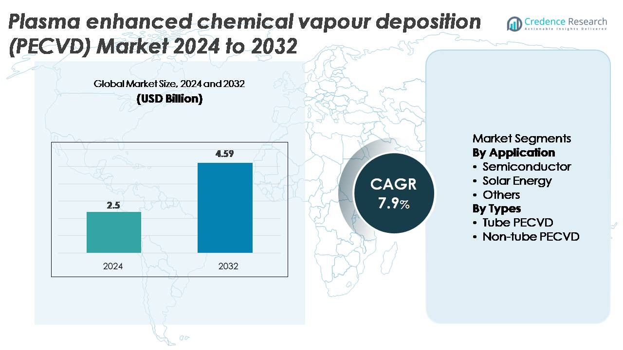
The global Plasma Enhanced Chemical Vapour Deposition (PECVD) units market was valued at USD 2.5 billion in 2024 and is projected to reach USD 4.59 billion by 2032, registering a CAGR of 7.9% during the forecast period.
| REPORT ATTRIBUTE |
DETAILS |
| Historical Period |
2020-2023 |
| Base Year |
2024 |
| Forecast Period |
2025-2032 |
| Plasma Enhanced Chemical Vapour Deposition (PECVD) units Market Size 2024 |
USD 2.5 Billion |
| Plasma Enhanced Chemical Vapour Deposition (PECVD) units Market, CAGR |
7.9% |
| Plasma Enhanced Chemical Vapour Deposition (PECVD) units Market Size 2032 |
USD 4.59 Billion |
The PECVD units market is shaped by strong participation from global equipment manufacturers such as Jusung Engineering, CVD Equipment, Piotech, ASM International, TES, SPTS Technologies (KLA), Wonik IPS, Applied Materials, Eugene Technology, and Lam Research, all of which compete through advancements in plasma stability, film uniformity, and high-throughput chamber designs. These companies serve high-growth sectors including semiconductors, photovoltaics, and thin-film electronics, reinforcing their positions through R&D investments and partnerships with major fabs. Asia-Pacific leads the market with approximately 45% share, driven by extensive wafer fabrication and solar module production, followed by North America at around 25%, supported by advanced semiconductor manufacturing expansion.
Access crucial information at unmatched prices!
Request your sample report today & start making informed decisions powered by Credence Research Inc.!
Download Sample
Market Insights
- The PECVD units market was valued at USD 2.5 billion in 2024 and is projected to reach USD 4.59 billion by 2032, registering a CAGR of 7.9%, supported by rising adoption in semiconductor and solar manufacturing.
- Demand strengthens as advanced nodes, 3D architectures, and high-efficiency PV technologies require precise thin-film deposition, making the semiconductor segment the dominant application, accounting for the largest share due to intensive use in dielectric and passivation layers.
- Trends such as expansion of flexible electronics, low-temperature deposition, and large-area processing accelerate technology upgrades and encourage investment in high-throughput, multi-chamber PECVD platforms.
- Competition intensifies among global players focusing on plasma uniformity, defect reduction, and digital process control, while high capital costs and complex integration requirements restrain adoption for small and mid-scale manufacturers.
- Asia-Pacific leads with ~45% market share, followed by North America (~25%) and Europe (~20%), driven respectively by large-scale fabs, domestic chip expansion, and strong PV and power-electronics innovation.
Market Segmentation Analysis:
By Application
The semiconductor segment holds the dominant share in the PECVD units market, driven by its critical role in depositing dielectric layers, passivation films, and barrier coatings for advanced logic and memory devices. Continuous node shrinkage, expansion of 3D architectures, and rising adoption of high-k materials strengthen demand for high-precision PECVD systems with superior uniformity and low defectivity. Solar energy applications also show steady growth as PECVD supports essential layers in heterojunction and passivated-emitter solar cells, while the “others” category gains traction from optics, medical devices, and thin-film sensors.
- “For instance, Applied Materials’ Producer® PECVD system supports highly uniformlow-temperature dielectric deposition, with some processes operating below 400 °C (as low as 100°C–350°C for advanced packaging applications), enabling integration in advanced FinFET and GAA structures.
By Types
Non-tube PECVD systems command the leading market share due to their suitability for large-area substrates, higher throughput, and integration into automated production lines for semiconductors, displays, and photovoltaic modules. Their ability to maintain stable plasma distribution over wide surfaces makes them preferred for mass manufacturing environments. Tube PECVD systems remain relevant in specialized research, small-batch production, and applications requiring superior control over deposition chemistry. However, increasing investments in large-scale electronics fabrication and thin-film solar technologies continue to reinforce non-tube PECVD as the dominant technology category.
- For instance, Applied Materials’ AKT-PECVD platform for display and solar applications supports glass substrates up to Gen-10.5 (3,370 × 2,940 mm) and delivers film-thickness uniformity below ±3 nm across the entire panel, a benchmark for large-format deposition.
Key Growth Drivers
Expansion of Semiconductor Fabrication and Advanced Node Scaling
The rapid advancement of semiconductor manufacturing remains the strongest catalyst for PECVD unit adoption, as fabs increasingly require highly uniform, low-defect thin films for 3D NAND, FinFET, GAA-FET, and advanced packaging architectures. As device geometries continue to shrink, PECVD systems are essential for depositing conformal dielectric layers, spacer materials, and passivation coatings while maintaining precise plasma control. Foundries’ massive investments in new fabs and technology nodes accelerate equipment demand, especially for high-throughput chambers designed for multi-layer deposition. The expansion of heterogeneous integration, chiplet-based designs, and advanced wafer-level packaging further intensifies the need for PECVD technologies that support complex stack engineering. This driver gains momentum as leading IDMs emphasize higher density, enhanced reliability, and improved electrical performance in next-generation chips.
- For instance, Lam Research’s VECTOR® PECVD platform supports up to 12 chambers with deposition rates exceeding 10,000 Å/min for SiN, allowing high-volume multi-layer stacking used in 200-plus layer 3D NAND.
Growing Demand for High-Efficiency Solar Photovoltaics
The solar energy sector significantly boosts PECVD equipment need, driven by the global shift toward higher-efficiency PV technologies such as heterojunction (HJT), passivated emitter rear cell (PERC), and TOPCon architectures. PECVD systems are essential for depositing intrinsic and doped silicon layers, anti-reflective coatings, and surface passivation films that directly influence conversion efficiency. As manufacturers transition to gigawatt-scale production lines, they increasingly rely on PECVD tools capable of large-area deposition with strong film uniformity. The rise in utility-scale and rooftop solar installations accelerates demand for advanced PECVD platforms that enable higher module performance, extended service life, and reduced light-induced degradation. The trend toward next-generation PV cells further reinforces PECVD’s strategic importance in solar manufacturing ecosystems.
- For instance, Jusung Engineering’s HJT PECVD production line is publicly documented to process up to 4,000 M6 wafers per hour at deposition temperatures below 200 °C, enabling ultra-thin (~10–20 nm) intrinsic a-Si layers critical for high-efficiency heterojunction cells.
Rapid Adoption of Thin-Film Technologies Across Emerging Industries
Emerging applications in optics, displays, sensors, medical devices, and protective coatings expand PECVD usage beyond traditional markets. The technology’s ability to deposit high-quality barrier films, hydrophobic coatings, and low-temperature layers makes it essential for flexible electronics, OLED displays, micro-sensors, and specialized biomedical components. Industries adopting miniaturized, lightweight, and durable devices increasingly prefer PECVD because it enables precise film engineering on diverse substrates, including polymers and temperature-sensitive materials. Growth is further supported by rising demand for anti-scratch, anti-fog, and moisture-resistant coatings across automotive, wearable devices, and industrial applications. As innovation accelerates in micro-electromechanical systems (MEMS) and emerging high-frequency communication devices, PECVD continues to serve as a foundational deposition method for surface modification and functional layer development.
Key Trends & Opportunities
Shift Toward Large-Area Deposition and High-Throughput Manufacturing
A major trend in the PECVD market is the transition toward equipment capable of large-area deposition to support high-volume manufacturing in semiconductors, photovoltaics, and displays. Manufacturers increasingly prioritize multi-chamber, cluster, and inline PECVD platforms that deliver higher throughput while maintaining strict uniformity standards. This shift creates opportunities for vendors offering scalable system architectures and advanced plasma control technologies. The demand for 300 mm and larger wafer formats, alongside gigawatt-scale solar module lines, positions high-throughput PECVD systems as essential to cost optimization. Additionally, innovations in process automation, real-time diagnostics, and AI-enabled chamber monitoring enhance uptime and yield, creating new growth avenues for equipment suppliers.
· For instance, Lam Research’s VECTOR® PECVD platform supports configurations with up to 12 chambers and delivers SiN deposition rates in the 10,000 Å/min class, allowing high-volume multi-stack dielectric formation used in 200-plus-layer 3D NAND fabrication.
Advancements in Low-Temperature and Flexible Substrate Deposition
The market is witnessing strong opportunities in low-temperature PECVD processes designed for flexible electronics, polymer substrates, and emerging device formats. As demand rises for foldable displays, thin-film wearables, and flexible sensors, PECVD systems capable of depositing functional films at reduced temperatures gain strategic relevance. This trend is encouraging manufacturers to develop plasma sources, precursor chemistries, and chamber designs that minimize thermal stress while ensuring high film quality. Opportunities expand further as industries pursue lightweight, bendable, and transparent components that require PECVD-based barrier layers, dielectric coatings, and encapsulation films. The convergence of flexible device innovation and low-temperature processing creates a strong multi-year growth pathway.
· For instance, Jusung Engineering’s HJT PECVD production line operates below 200 °C and processes up to 4,000 M6 wafers per hour, enabling deposition of 10–20 nm intrinsic a-Si layers needed for high-efficiency heterojunction solar cells.
Increasing Integration of Digital Process Control and Predictive Maintenance
Advanced software and digitalization trends are reshaping PECVD equipment design, enabling higher process stability, improved repeatability, and reduced operational cost. AI-driven analytics, machine learning algorithms, and digital twins are increasingly deployed to monitor plasma behavior, detect anomalies, and predict maintenance needs in real time. These advancements help fabs reduce downtime, improve yield, and extend equipment life. As manufacturers prioritize smart manufacturing and Industry 4.0 strategies, PECVD suppliers offering integrated data platforms and intelligent control systems stand to gain significant competitive advantage. This trend creates strong opportunities for service-based revenue models and long-term performance optimization partnerships.
Key Challenges
High Capital Expenditure and Complex Integration Requirements
One of the most significant challenges for the PECVD market is the high capital investment required for advanced deposition equipment, particularly for multi-chamber cluster systems used in semiconductor fabrication. Smaller manufacturers and emerging solar producers often face financial constraints that limit adoption of state-of-the-art PECVD platforms. Additionally, integrating PECVD modules into existing production lines requires sophisticated facility infrastructure, advanced cleanroom conditions, and skilled process engineers. These complexities increase installation time, operational costs, and maintenance overhead. As technology nodes advance, process recipes grow more intricate, further raising the barrier to entry for cost-sensitive industries and new market participants.
Process Sensitivity, Material Compatibility Issues, and Plasma-Induced Damage
PECVD processes are highly sensitive to plasma density, gas flow dynamics, precursor selection, and substrate conditions, making consistent film quality challenging without stringent process control. Achieving uniform deposition across large substrates or complex device structures requires advanced plasma tuning that not all manufacturers can easily optimize. Certain materials, particularly temperature-sensitive polymers or delicate semiconductor layers, face risks of plasma-induced damage, affecting device performance. Managing these compatibility challenges demands continuous engineering improvements, sophisticated chamber designs, and precise process parameter optimization. For manufacturers unable to meet these exacting requirements, yield losses and performance variability remain major operational hurdles.
Regional Analysis
North America
North America holds around 25% of the PECVD units market, supported by strong semiconductor manufacturing activity and sustained investments in advanced logic and memory production. The U.S. leads with major fabs expanding capacity for 300 mm wafer processing, strengthening demand for high-precision PECVD platforms. Growth is further reinforced by federal incentives for domestic chip production and increasing adoption of thin-film technologies in aerospace, medical devices, and optical coatings. Canada contributes through research-focused thin-film development and niche electronics manufacturing, collectively maintaining the region’s position as a high-value PECVD equipment buyer.
Europe
Europe accounts for nearly 20% of the global market, driven by robust growth in automotive electronics, power semiconductors, and photovoltaic research. Germany, France, and the Netherlands anchor PECVD adoption through innovation in wide-bandgap devices, MEMS production, and thin-film solar technologies. Strong emphasis on energy-efficient manufacturing and next-generation PV cells supports demand for advanced deposition systems. The region’s technical universities and R&D institutes also contribute significantly by driving process innovation. Additionally, Europe’s focus on industrial automation and EV power electronics expands the need for high-uniformity PECVD units across diverse applications.
Asia-Pacific
Asia-Pacific dominates the market with an estimated 45% share, led by aggressive semiconductor expansion in China, Taiwan, South Korea, and Japan. High-volume fabrication, rapid technology node transitions, and large-scale solar module manufacturing create strong, sustained demand for PECVD units. China’s investments in domestic wafer fabs and Korea’s leadership in memory production further accelerate market growth. The region also leads in thin-film electronics, flexible displays, and high-efficiency photovoltaic cells, requiring sophisticated PECVD platforms. Strategic government incentives and cost-competitive manufacturing ecosystems reinforce Asia-Pacific’s position as the global hub for deposition equipment consumption.
Latin America
Latin America holds a modest 5% share, driven by growing adoption of PECVD systems in solar energy deployment and emerging electronics assembly sectors. Brazil, Mexico, and Chile are the primary markets, benefiting from increased investments in renewable energy infrastructure and thin-film PV module integration. Although semiconductor manufacturing remains limited, regional demand is supported by applications in coatings, sensors, and industrial components. Collaborative R&D programs with international equipment suppliers are helping local industries access advanced thin-film deposition capabilities. The region’s gradual increase in technology diversification is expected to create incremental opportunities for PECVD solutions.
Middle East & Africa
The Middle East & Africa region contributes around 5% to the global PECVD market, with growth primarily fueled by renewable energy investments, particularly in thin-film solar technologies. Countries such as the UAE, Saudi Arabia, and South Africa are integrating PECVD-based PV components to support large-scale solar farm development. The electronics manufacturing base remains small, but increasing adoption of advanced coating technologies in aerospace, energy, and industrial sectors drives niche demand. Research collaborations and technology transfer initiatives are gradually expanding regional process capabilities, positioning MEA as an emerging but steadily developing PECVD market.
Market Segmentations:
By Application
- Semiconductor
- Solar Energy
- Others
By Types
- Tube PECVD
- Non-tube PECVD
By Geography
- North America
- Europe
- Germany
- France
- U.K.
- Italy
- Spain
- Rest of Europe
- Asia Pacific
- China
- Japan
- India
- South Korea
- South-east Asia
- Rest of Asia Pacific
- Latin America
- Brazil
- Argentina
- Rest of Latin America
- Middle East & Africa
- GCC Countries
- South Africa
- Rest of the Middle East and Africa
Competitive Landscape
The competitive landscape of the PECVD units market is defined by a mix of global semiconductor equipment manufacturers and specialized deposition system providers competing on process precision, throughput, and large-area capability. Leading companies focus on developing multi-chamber architectures, advanced plasma sources, and AI-driven process control to meet the demands of sub-10 nm semiconductor nodes, high-efficiency solar cells, and emerging thin-film electronics. Major players strengthen their positions through strategic collaborations with leading foundries and photovoltaic producers, enabling co-development of optimized deposition recipes. Investments in low-temperature PECVD for flexible electronics and large-format systems for gigawatt-scale solar lines further intensify competition. Vendors also differentiate through enhanced service models, predictive maintenance platforms, and modular system designs that enable scalability across diverse applications. As the market expands into advanced packaging, wide-bandgap power devices, and flexible wearables, suppliers with strong R&D capabilities and high-volume manufacturing expertise continue to secure a competitive advantage.
Shape Your Report to Specific Countries or Regions & Enjoy 30% Off!
Key Player Analysis
Recent Developments
- In October 2025, CVD Equipment Corporation it obtained an order for two of its PVT150™ systems, reflecting continuing demand for its thermal/deposition equipment.
- In May 2024, Jusung announced a corporate restructure: it decided to spin off its semiconductor, solar, and display divisions into separate entities. The reorganization aims to let the semiconductor-equipment division focus exclusively on technology development and manufacturing, presumably including its PECVD and related deposition tool portfolio.
Report Coverage
The research report offers an in-depth analysis based on Application, Type and Geography. It details leading market players, providing an overview of their business, product offerings, investments, revenue streams, and key applications. Additionally, the report includes insights into the competitive environment, SWOT analysis, current market trends, as well as the primary drivers and constraints. Furthermore, it discusses various factors that have driven market expansion in recent years. The report also explores market dynamics, regulatory scenarios, and technological advancements that are shaping the industry. It assesses the impact of external factors and global economic changes on market growth. Lastly, it provides strategic recommendations for new entrants and established companies to navigate the complexities of the market.
Future Outlook
- Demand for PECVD units will rise as advanced semiconductor nodes and 3D device architectures require higher precision in dielectric and passivation layer deposition.
- Solar PV manufacturers will increasingly adopt PECVD for high-efficiency cell technologies such as HJT, TOPCon, and next-generation passivation layers.
- Low-temperature PECVD processes will gain traction to support flexible, wearable, and polymer-based electronics.
- Large-area deposition systems will see stronger adoption in display manufacturing, thin-film modules, and high-throughput production lines.
- AI-enabled process control and predictive maintenance will become critical for improving yield and uptime across fabs.
- Material innovations and new precursor chemistries will expand PECVD applicability in optics, sensors, and MEMS devices.
- Equipment vendors will focus on modular, scalable platforms to meet diverse industry requirements and shorten installation timelines.
- Sustainability initiatives will drive interest in PECVD processes that reduce energy consumption and enhance chamber efficiency.
- Regional manufacturing expansion, especially in Asia-Pacific, will continue to shape competitive dynamics and supply chain strategies.
- Collaborative development between equipment makers and device manufacturers will accelerate customized PECVD process recipes for complex multilayer stacks.