Market Overview
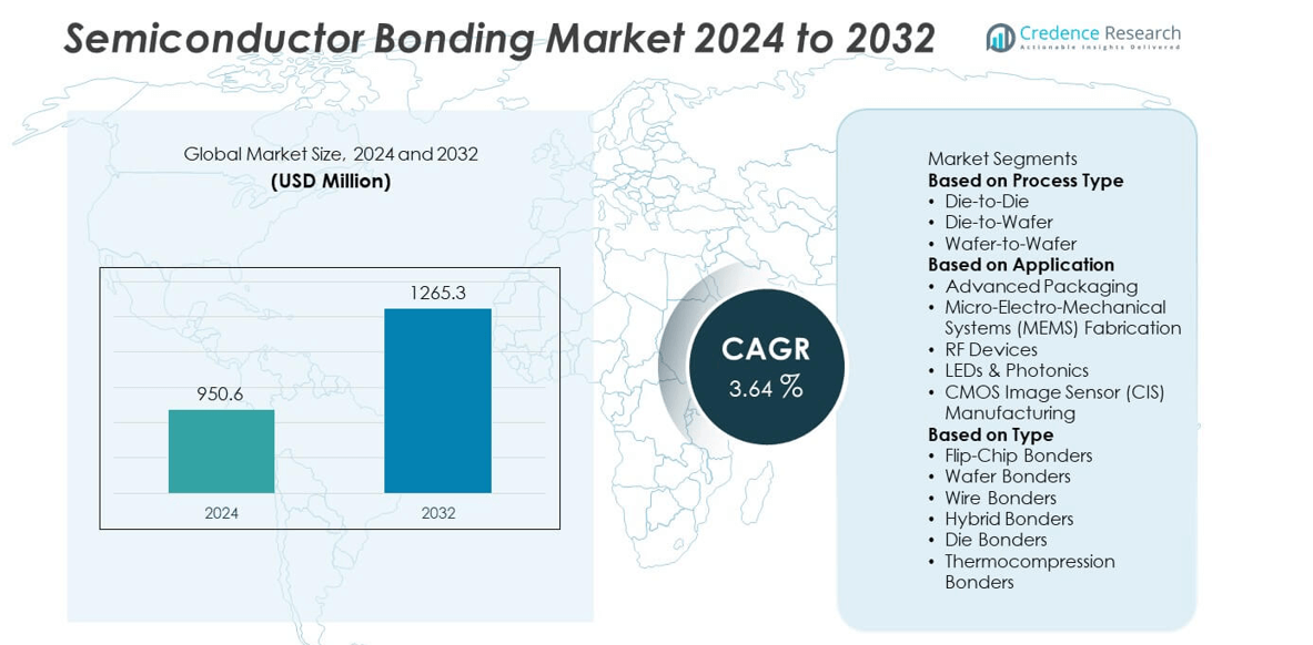
The Semiconductor Bonding Market was valued at USD 950.6 million in 2024 and is anticipated to reach USD 1,265.3 million by 2032, growing at a CAGR of 3.64% during the forecast period.
| REPORT ATTRIBUTE |
DETAILS |
| Historical Period |
2020-2023 |
| Base Year |
2024 |
| Forecast Period |
2025-2032 |
| Semiconductor Bonding Market Size 2024 |
USD 950.6 million |
| Semiconductor Bonding Market, CAGR |
3.64% |
| Semiconductor Bonding Market Size 2032 |
USD 1,265.3 million |
The Semiconductor Bonding Market grows through strong demand for miniaturized consumer electronics, electric vehicles, and advanced computing devices. It benefits from the rising need for precision bonding in smartphones, wearables, and 5G infrastructure, ensuring reliability and energy efficiency.
The Semiconductor Bonding Market demonstrates strong geographical presence across Asia-Pacific, North America, Europe, Latin America, and the Middle East & Africa, each contributing to its global expansion. Asia-Pacific leads as the hub of semiconductor manufacturing, driven by large-scale production in Taiwan, South Korea, China, and Japan, with strong demand from consumer electronics, 5G infrastructure, and automotive semiconductors. North America follows with advanced R&D facilities and adoption in automotive, aerospace, and high-performance computing applications. Europe emphasizes bonding solutions in automotive electronics, renewable energy systems, and industrial automation, while Latin America and the Middle East & Africa show gradual growth through industrial diversification and digital infrastructure development. Key players shaping the market include EV Group (EVG), a leader in wafer bonding technologies; Besi, specializing in advanced packaging and hybrid bonding; Kulicke and Soffa Industries, Inc., known for wire bonding systems; and ASMPT, delivering a broad range of assembly and packaging solutions.
Access crucial information at unmatched prices!
Request your sample report today & start making informed decisions powered by Credence Research Inc.!
Download Sample
Market Insights
- The Semiconductor Bonding Market was valued at USD 950.6 million in 2024 and is projected to reach USD 1,265.3 million by 2032, growing at a CAGR of 3.64% during the forecast period.
- Growth is driven by rising demand for miniaturized consumer electronics, wearables, and advanced IoT devices that require precise bonding technologies to ensure performance and durability.
- Market trends highlight increasing adoption of wafer-level, hybrid, and 3D integration technologies, along with automation and AI-driven monitoring systems that enhance productivity and accuracy.
- Competitive dynamics are shaped by leading players such as EV Group (EVG), Besi, Kulicke and Soffa Industries, ASMPT, and Panasonic Connect, who focus on advanced packaging and bonding precision.
- Restraints include high capital investment, complex manufacturing requirements, and a shortage of skilled workforce, which create barriers for smaller manufacturers and slow widespread adoption.
- Regional growth is led by Asia-Pacific with large-scale semiconductor hubs in Taiwan, South Korea, China, and Japan, followed by North America with advanced R&D facilities and Europe with strong automotive and renewable energy applications.
- The market reflects a growing shift toward sustainability and energy-efficient bonding systems, as vendors invest in greener technologies and predictive maintenance features to meet environmental and operational goals.
Market Drivers
Rising Demand for Compact and High-Performance Consumer Devices
The Semiconductor Bonding Market grows with the rising adoption of smartphones, tablets, and wearables that require smaller and faster chips. Bonding technologies ensure high interconnect density while maintaining performance in compact designs. It allows manufacturers to deliver devices with better speed, reduced power consumption, and durability. Consumer expectations for sleek designs with advanced features drive continuous innovation in bonding processes. Vendors focus on precision bonding systems that handle ultra-thin wafers for reliable performance. Strong demand in consumer electronics keeps bonding at the center of semiconductor production.
- For instance, In 2018 EVG unveiled an upgraded version of the bonder, featuring the new SmartView® NT3 aligner. This improved alignment accuracy to sub-50 nm for demanding high-volume applications, including BSI CMOS image sensor stacking.
Expansion of Automotive Electronics and Electric Vehicle Adoption
Automotive applications fuel semiconductor demand across infotainment, driver-assistance, and battery management systems. The Semiconductor Bonding Market benefits as electric vehicles rely on durable power devices and sensors. It enables precise chip bonding that withstands high temperatures and harsh automotive conditions. Growth in EVs accelerates investment in advanced bonding systems for energy conversion and safety-critical electronics. Automakers require high-reliability semiconductors for autonomous and connected vehicle functions. This driver ensures consistent demand from one of the fastest-growing end-use industries.
- For instance, In April 2025, Besi announced a strategic partnership with Applied Materials to further develop integrated hybrid bonding systems. This partnership aims to deliver sub-5 μm alignment accuracy and high-throughput production.
Strong Push from 5G Infrastructure and Data-Centric Applications
The rollout of 5G and expansion of data centers create robust demand for high-bandwidth and low-latency chips. The Semiconductor Bonding Market supports this trend with equipment designed for RF modules, processors, and memory devices. It provides the accuracy required for packaging chips used in cloud computing and AI workloads. Advanced bonding methods enhance speed, density, and energy efficiency in complex devices. Vendors innovate to support seamless integration of logic and memory components. Increasing reliance on real-time data strengthens long-term growth for bonding solutions.
Adoption of Advanced Packaging and 3D Integration Technologies
Semiconductor packaging advances with wafer-to-wafer bonding, die-to-wafer bonding, and system-in-package methods. The Semiconductor Bonding Market grows by enabling heterogeneous integration where memory, processors, and sensors are combined in one chip. It improves performance while reducing size and ensuring thermal stability. Advanced bonding supports multifunctional devices required in healthcare, aerospace, and industrial automation. Vendors focus on hybrid bonding solutions to meet growing design complexity. This push toward 3D integration secures bonding as a critical enabler of next-generation semiconductor applications.
Market Trends
Shift Toward Wafer-Level and Hybrid Bonding Technologies
Manufacturers are adopting wafer-level and hybrid bonding to address increasing miniaturization requirements. The Semiconductor Bonding Market supports these processes by providing equipment capable of ultra-fine alignment and reliable interconnects. It enables higher chip density, faster processing, and lower power consumption for advanced applications. Hybrid bonding is gaining traction for its ability to integrate memory and logic chips seamlessly. Vendors enhance throughput and accuracy to meet the complex needs of next-generation devices. This trend positions bonding as a central element in advanced packaging.
- For instance, Besi announced that its hybrid bonding systems are on track to ship with an alignment accuracy of 50 nm in 2025, and are already achieving speeds exceeding 3,000 units per hour (UPH). These systems are central to supporting AI and high-bandwidth memory applications.
Integration of Automation and Smart Manufacturing
Automation drives efficiency in semiconductor production lines, reducing error rates and increasing yield. The Semiconductor Bonding Market reflects this trend with systems that incorporate robotics, sensors, and AI-driven monitoring. It helps manufacturers achieve consistent quality while lowering production costs. Predictive maintenance capabilities improve uptime and extend equipment life. Automated bonding also ensures precision in high-volume production environments. Vendors focus on scalable solutions that align with smart manufacturing strategies across the industry.
- For instance, ASMPT introduced its INFINITE die bonder with AI-based predictive control, capable of handling over 10,000 die placements per hour while reducing misalignment defects to below 0.05%.
Growing Adoption of 3D Integration and System-in-Package Designs
Demand for compact, multifunctional chips accelerates the use of 3D integration and system-in-package technologies. The Semiconductor Bonding Market adapts by offering solutions that support vertical stacking and heterogeneous integration. It allows the combination of sensors, logic, and memory within one package, improving performance and efficiency. These designs are vital for applications in AI, edge computing, and high-performance devices. Vendors develop tools that address interconnect density and thermal management challenges. This trend strengthens the role of bonding in complex semiconductor architectures.
Focus on Energy Efficiency and Sustainable Production
Sustainability influences technology adoption across the semiconductor sector. The Semiconductor Bonding Market responds by developing equipment that reduces material waste and energy use. It helps manufacturers meet regulatory and environmental targets while maintaining high productivity. Energy-efficient bonding systems also lower long-term operational costs. Vendors highlight greener technologies as a competitive advantage in global markets. The push toward sustainable practices ensures bonding remains aligned with industry-wide environmental goals.
Market Challenges Analysis
High Equipment Costs and Complex Manufacturing Requirements
The Semiconductor Bonding Market faces challenges due to the high capital required for advanced bonding systems. It demands equipment capable of extreme precision and scalability, which increases procurement and operational costs. Smaller companies find it difficult to invest in such technologies, limiting widespread adoption. Complex manufacturing requirements, such as handling ultra-thin wafers and ensuring alignment accuracy, add further difficulty. Vendors must balance innovation with affordability to encourage adoption across both large enterprises and smaller players. These financial and technical hurdles restrict the market’s ability to expand rapidly.
Supply Chain Disruptions and Skilled Workforce Shortages
Global supply chain instability impacts timely availability of semiconductor bonding equipment and spare components. The Semiconductor Bonding Market is sensitive to fluctuations in raw materials and logistics disruptions, which can delay deliveries. It also struggles with a shortage of highly skilled professionals capable of operating and maintaining advanced bonding systems. Workforce limitations reduce production efficiency and increase training costs for manufacturers. Vendors and industry players must address these workforce and supply chain issues to maintain reliability. Overcoming these challenges is essential for the industry to sustain growth and competitiveness.
Market Opportunities
Rising Demand from Electric Vehicles and Renewable Energy Applications
The Semiconductor Bonding Market gains strong opportunities from the expansion of electric vehicles and renewable energy systems. It supports the production of power semiconductors essential for battery management, charging infrastructure, and energy conversion units. Governments and private players are investing heavily in clean energy technologies, increasing the need for durable and efficient chips. Wide bandgap materials such as silicon carbide and gallium nitride require precise bonding solutions to optimize power handling. Vendors offering specialized bonding systems for these applications can secure long-term contracts with automotive and energy firms. The growing global shift toward sustainability strengthens the role of bonding in next-generation applications.
Expansion of Advanced Packaging for AI, 5G, and Healthcare Devices
The Semiconductor Bonding Market benefits from the rising demand for high-performance chips in AI, 5G, and healthcare industries. It enables packaging solutions that deliver low latency, high bandwidth, and energy efficiency in compact chip designs. AI accelerators, 5G modules, and medical imaging devices require advanced bonding to ensure reliability. Vendors innovate with wafer-level and 3D integration tools tailored to these applications. Healthcare technologies such as wearable monitors and diagnostic systems also expand opportunities for bonding solutions. Companies that align equipment development with these industries gain a strategic edge in the global market.
Market Segmentation Analysis:
By Process Type
The Semiconductor Bonding Market is segmented into die-to-die, die-to-wafer, and wafer-to-wafer processes. Die-to-die bonding remains significant where strong interconnections and high alignment accuracy are critical for logic devices and memory chips. It is widely used in compact semiconductor designs that require multiple layers of performance. Die-to-wafer bonding gains momentum with the adoption of heterogeneous integration, enabling the combination of different chip functions in one package. Wafer-to-wafer bonding holds a vital role in advanced packaging and 3D integration, supporting high-density applications such as smartphones, sensors, and memory devices. Vendors continue to refine throughput and precision across all three bonding processes to support complex semiconductor requirements.
- For instance, The EVG GEMINI® FB XT system now achieves sub-50 nm wafer-to-wafer alignment, which is an improvement over the previous generation. The system is optimized for high-volume manufacturing, with throughput of up to 20 wafers per hour. It supports the production of advanced 3D-IC devices.
By Application
Applications in the Semiconductor Bonding Market span advanced packaging, MEMS fabrication, RF devices, LEDs and photonics, CMOS image sensors, and power electronics. Advanced packaging dominates demand, supported by growth in 3D integration, wafer-level packaging, and system-in-package technologies. MEMS fabrication expands usage as bonding supports miniaturized sensors used in automotive, industrial, and healthcare applications. RF devices rely on precise bonding to perform efficiently in 5G modules and high-frequency applications. LEDs and photonics benefit from bonding processes that enhance reliability and heat management in lighting and display technologies. CMOS image sensors, widely used in smartphones and automotive cameras, also strengthen adoption. Power electronics represent another vital segment, supported by electric vehicles and renewable energy systems.
- For instance, Kulicke & Soffa offers ProVertical and ProCascade Loop technologies, designed for high-density vertical and cascade wire interconnects in advanced memory applications. This technology is part of its ATPremier MEM PLUS™ platform, which is specifically engineered to meet the performance needs of high-volume, at-the-edge AI and memory devices.
By Type
The Semiconductor Bonding Market includes flip-chip bonders, wafer bonders, wire bonders, hybrid bonders, die bonders, and thermocompression bonders. Flip-chip bonders remain important for high-speed interconnections in processors, GPUs, and networking devices. Wafer bonders gain demand for memory and logic devices that require accurate alignment of ultra-thin wafers. Wire bonders maintain widespread use in traditional packaging for consumer electronics and automotive chips. Hybrid bonders represent the fastest-growing category, enabling advanced 3D packaging and integration of multiple components into one chip. Die bonders continue to dominate production lines for consumer and automotive applications where throughput and accuracy are essential. Thermocompression bonders see adoption in specialized applications that require durable and high-temperature bonding. Vendors focus on advancing automation, accuracy, and scalability across all equipment categories.
Shape Your Report to Specific Countries or Regions & Enjoy 30% Off!
Segments:
Based on Process Type
- Die-to-Die
- Die-to-Wafer
- Wafer-to-Wafer
Based on Application
- Advanced Packaging
- Micro-Electro-Mechanical Systems (MEMS) Fabrication
- RF Devices
- LEDs & Photonics
- CMOS Image Sensor (CIS) Manufacturing
Based on Type
- Flip-Chip Bonders
- Wafer Bonders
- Wire Bonders
- Hybrid Bonders
- Die Bonders
- Thermocompression Bonders
Based on the Geography:
- North America
- Europe
- UK
- France
- Germany
- Italy
- Spain
- Russia
- Belgium
- Netherlands
- Austria
- Sweden
- Poland
- Denmark
- Switzerland
- Rest of Europe
- Asia Pacific
- China
- Japan
- South Korea
- India
- Australia
- Thailand
- Indonesia
- Vietnam
- Malaysia
- Philippines
- Taiwan
- Rest of Asia Pacific
- Latin America
- Brazil
- Argentina
- Peru
- Chile
- Colombia
- Rest of Latin America
- Middle East
- UAE
- KSA
- Israel
- Turkey
- Iran
- Rest of Middle East
- Africa
- Egypt
- Nigeria
- Algeria
- Morocco
- Rest of Africa
Regional Analysis
Asia-Pacific
Asia-Pacific dominates the Semiconductor Bonding Market with a share of about 40% in 2024, making it the largest regional contributor. The region benefits from strong semiconductor production hubs in Taiwan, South Korea, China, and Japan. It supports large-scale adoption of wafer-to-wafer and die-to-wafer bonding technologies for logic, memory, and CMOS image sensors. Growing demand from consumer electronics, 5G infrastructure, and automotive semiconductors drives continuous investment in bonding tools. Companies in the region focus on high-volume manufacturing with advanced bonding precision to maintain global competitiveness. Government-backed programs and foreign investments in semiconductor fabrication further reinforce Asia-Pacific’s leadership position in bonding technologies.
North America
North America accounts for around 28% of the Semiconductor Bonding Market in 2024, supported by advanced research facilities and strong demand across industries. The region leads in the adoption of high-performance bonding solutions for data centers, aerospace, and defense. Electric vehicles and advanced driver-assistance systems also increase demand for power semiconductors that require precise bonding. Companies in the United States invest heavily in hybrid bonding and wafer-level packaging to align with the growing AI and cloud computing markets. North America maintains a competitive edge through robust R&D infrastructure and focus on smart manufacturing solutions. Strong collaboration between equipment vendors and integrated device manufacturers strengthens regional innovation.
Europe
Europe represents about 20% of the Semiconductor Bonding Market in 2024, driven by its strong automotive and industrial base. The region emphasizes bonding technologies for power devices used in electric vehicles and renewable energy applications. Germany, France, and Italy lead adoption as automakers integrate advanced electronics into vehicle platforms. European policies, such as the European Chips Act, stimulate semiconductor investment and create new opportunities for equipment vendors. Bonding equipment is also used in healthcare and photonics applications, enhancing regional diversification. Europe’s focus on sustainable production and compliance with environmental standards supports demand for energy-efficient bonding solutions.
Latin America
Latin America contributes approximately 7% of the Semiconductor Bonding Market in 2024, reflecting gradual but steady adoption. Brazil and Mexico serve as the key growth drivers with expansion in automotive and consumer electronics manufacturing. Regional companies increasingly integrate bonding technologies to align with global semiconductor supply chains. Investments in renewable energy projects also create demand for power semiconductors requiring advanced bonding solutions. Though smaller in share, the region shows potential for long-term growth with rising foreign investments. Vendors entering Latin America focus on providing cost-effective bonding systems tailored to local industrial needs.
Middle East & Africa
The Middle East & Africa hold about 5% of the Semiconductor Bonding Market in 2024, making it the smallest regional segment. The region is at an early stage of semiconductor adoption, with demand largely from telecommunications, oil and gas, and industrial automation. Gulf Cooperation Council countries invest in technology parks and semiconductor research as part of economic diversification strategies. South Africa emerges as another contributor, particularly in automotive and renewable energy applications. Gradual improvements in infrastructure and digital transformation policies increase opportunities for bonding equipment adoption. While current market share is modest, steady growth is expected as the region builds industrial capacity.
Key Player Analysis
- Palomar Technologies
- EV Group (EVG)
- ASMPT
- Besi
- TDK Corporation
- Kulicke and Soffa Industries, Inc.
- Tokyo Electron Limited
- Panasonic Connect Co., Ltd.
- SHIBAURA MECHATRONICS CORPORATION
- Intel Corporation
Competitive Analysis
The competitive landscape of the Semiconductor Bonding Market is shaped by leading players including EV Group (EVG), Besi, Kulicke and Soffa Industries, ASMPT, Panasonic Connect, Palomar Technologies, SHIBAURA MECHATRONICS CORPORATION, Tokyo Electron Limited, TDK Corporation, and Intel Corporation. These companies focus on advancing wafer-to-wafer, die-to-wafer, and hybrid bonding technologies to meet the demands of miniaturization, high-density integration, and multifunctional chip designs. They invest heavily in research and development to deliver equipment with higher throughput, sub-micron alignment accuracy, and advanced thermal management capabilities. Strategic collaborations with foundries and outsourced assembly and test providers enable them to expand adoption across consumer electronics, automotive, and 5G applications. Vendors emphasize automation, robotics, and AI-enabled process monitoring to improve yields and reduce operational costs in high-volume manufacturing. Competitive strategies also include expansion into sustainable and energy-efficient bonding solutions to align with global environmental goals. Strong innovation pipelines, global partnerships, and focus on precision make these players central to driving competitiveness in the Semiconductor Bonding Market.
Recent Developments
- In July 2025, Panasonic announced the transition of its President and CEO effective April 2026.
- In May 2025, TDK earned recognition as part of Japan’s SX Brand 2025 for its leadership in sustainability transformation.
- In March 2025, Palomar moved its Advanced Solutions Division in Asia into a larger facility to meet growing demand for advanced microelectronics assembly services.
- In March 2025, EVG introduced its next-generation GEMINI® automated production wafer bonding system for 300‑mm wafers.
Report Coverage
The research report offers an in-depth analysis based on Process Type, Application, Type and Geography. It details leading market players, providing an overview of their business, product offerings, investments, revenue streams, and key applications. Additionally, the report includes insights into the competitive environment, SWOT analysis, current market trends, as well as the primary drivers and constraints. Furthermore, it discusses various factors that have driven market expansion in recent years. The report also explores market dynamics, regulatory scenarios, and technological advancements that are shaping the industry. It assesses the impact of external factors and global economic changes on market growth. Lastly, it provides strategic recommendations for new entrants and established companies to navigate the complexities of the market.
Future Outlook
- Hybrid and wafer-level bonding technologies will enable tighter chip integration and improved performance.
- Rising demand from AI-driven data centers will increase adoption of advanced bonding solutions.
- Automation with AI will enhance precision, raise throughput, and reduce production errors.
- Growth in 3D integration and system-in-package designs will expand bonding applications.
- Sustainability targets will drive the development of energy-efficient and low-waste bonding equipment.
- Asia-Pacific will strengthen its leadership as the global hub for bonding solutions.
- OSAT providers will boost demand for modular and flexible bonding systems.
- AI-powered defect detection will improve quality assurance and reduce manufacturing rework.
- Partnerships with foundries and IDMs will align bonding tools with next-generation packaging nodes.
- Localized manufacturing and supply chain resilience will shape equipment deployment strategies.


