Market Overview:
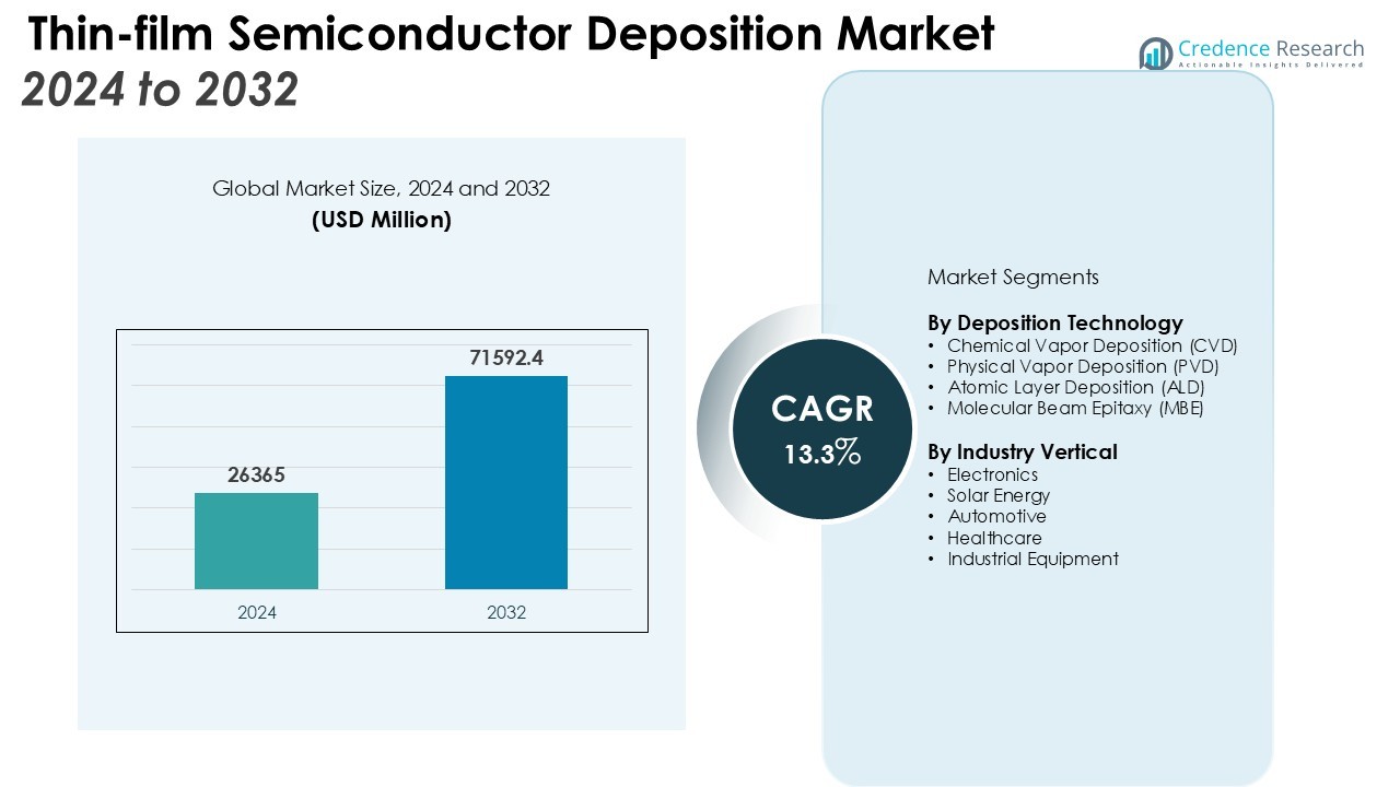
The Thin-film Semiconductor Deposition Market size was valued at USD 26365 million in 2024 and is anticipated to reach USD 71592.4 million by 2032, at a CAGR of 13.3% during the forecast period (2024-2032).
| REPORT ATTRIBUTE |
DETAILS |
| Historical Period |
2020-2024 |
| Base Year |
2024 |
| Forecast Period |
2025-2032 |
| Thin-film Semiconductor Deposition Market Size 2024 |
USD 26365 Million |
| Thin-film Semiconductor Deposition Market, CAGR |
13.3% |
| Thin-film Semiconductor Deposition Market Size 2032 |
USD 71592.4 Million |
Key drivers shaping the Thin-film Semiconductor Deposition Market include rising demand for high-performance microelectronics, robust growth in renewable energy installations—particularly thin-film solar cells—and rapid advances in display technologies. Expanding applications in IoT devices, automotive electronics, and medical equipment further accelerate market adoption. Manufacturers invest heavily in process improvements and next-generation materials to achieve superior device functionality, reliability, and energy efficiency, fostering a competitive and dynamic landscape.
Regionally, Asia Pacific leads the Thin-film Semiconductor Deposition Market, accounting for the largest revenue share due to its strong base of semiconductor manufacturing hubs in China, South Korea, Taiwan, and Japan. North America and Europe also contribute significantly, supported by strategic investments in R&D and strong demand from the electronics and renewable energy sectors. The market also witnesses growing participation from emerging economies as governments introduce initiatives to localize semiconductor manufacturing and strengthen supply chains.
Access crucial information at unmatched prices!
Request your sample report today & start making informed decisions powered by Credence Research Inc.!
Download Sample
Market Insights:
- The Thin-film Semiconductor Deposition Market reached USD 26,365 million in 2024 and is projected to hit USD 71,592 million by 2032, registering a CAGR of 13.3% from 2024 to 2032.
- Rising adoption of high-performance consumer electronics and wearables continues to drive robust demand for thin-film semiconductor components globally.
- Expansion of renewable energy projects, especially solar photovoltaics, increases the requirement for advanced thin-film deposition technologies across major economies.
- Technological progress in OLED, micro-LED, and flexible display applications fosters new opportunities for thin-film semiconductor manufacturers.
- The market faces challenges from high capital investments, complex process requirements, and material compatibility issues impacting yield and production scalability.
- Asia Pacific leads the global market with 55% revenue share, followed by North America at 24% and Europe at 15%, supported by strong manufacturing ecosystems and policy support.
- Growing government initiatives and collaboration across technology providers and manufacturers stimulate localization of semiconductor manufacturing and strengthen supply chains in emerging regions.
Market Drivers:
Rising Adoption of High-Performance Consumer Electronics Accelerates Market Demand
The Thin-film Semiconductor Deposition Market benefits significantly from the increasing penetration of advanced consumer electronics worldwide. The proliferation of smartphones, tablets, and wearable devices has raised the need for compact, high-performance semiconductor components. Manufacturers rely on thin-film deposition technologies to achieve device miniaturization, improved functionality, and superior energy efficiency. The growing trend of smart home and entertainment systems further amplifies demand for reliable thin-film semiconductor solutions.
Expansion of Renewable Energy Projects Drives Thin-film Semiconductor Deposition
Global investment in renewable energy, particularly solar photovoltaics, is a primary driver for the Thin-film Semiconductor Deposition Market. Thin-film deposition processes are crucial for fabricating high-efficiency solar cells that support large-scale solar projects. The push toward decarbonization and stringent emission regulations encourage governments and private enterprises to expand solar infrastructure. It supports steady demand for advanced deposition technologies that deliver improved performance and reduced material costs.
Technological Advancements in Display and Sensor Technologies Propel Growth
Rapid innovations in display and sensor technologies further stimulate the Thin-film Semiconductor Deposition Market. Developments in OLED, micro-LED, and flexible display applications require advanced thin-film layers to enhance device brightness, resolution, and durability. It enables manufacturers to deliver next-generation screens and sensors for use in premium consumer electronics, automotive displays, and industrial equipment. Ongoing R&D fosters the integration of novel materials and more efficient deposition processes.
- For instance, high-performance Thin-Film Encapsulation (TFE) layers are deposited at low temperatures, often less than 100°C, to protect sensitive OLED materials from damage.
Increasing Applications in IoT, Automotive, and Medical Electronics Fuel Market Expansion
The evolution of the Internet of Things (IoT), connected vehicles, and smart healthcare devices broadens the scope of the Thin-film Semiconductor Deposition Market. The need for reliable, miniaturized, and energy-efficient semiconductors is critical in these rapidly evolving sectors. It supports the development of sensors, microcontrollers, and communication modules for diverse applications. Growing collaboration between technology providers and manufacturers ensures a robust pipeline of new products across these end-use industries.
- For example, Abbott’s FreeStyle Libre 3, a leading continuous glucose monitor, utilizes advanced semiconductor processes to achieve high accuracy in a compact device.
Market Trends:
Emergence of Advanced Deposition Techniques and Material Innovations is Reshaping the Market Landscape
The Thin-film Semiconductor Deposition Market is witnessing significant transformation with the introduction of advanced deposition techniques such as atomic layer deposition (ALD), molecular beam epitaxy (MBE), and plasma-enhanced chemical vapor deposition (PECVD). These technologies enable precise control over film thickness and composition, supporting the production of highly reliable semiconductor devices. Innovations in materials, including the use of compound semiconductors, organic thin films, and flexible substrates, drive the development of next-generation electronics. It encourages manufacturers to diversify product portfolios and address the demand for smaller, faster, and more energy-efficient components. Continuous advancements in deposition processes enable improved yield rates and reduced manufacturing costs, enhancing competitiveness across the value chain.
- For instance, by using a proprietary organic semiconductor material, Sony developed a super-flexible, full-color OLED display just 80 micrometers thick.
Integration of Thin-film Semiconductors in Emerging Applications Expands Growth Opportunities
The Thin-film Semiconductor Deposition Market is experiencing a surge in demand due to the growing integration of thin-film semiconductors in diverse applications. The adoption of flexible and transparent electronics, wearable medical devices, and automotive sensors broadens the market’s reach and application landscape. Increasing investments in research and development enable breakthroughs in flexible displays, transparent conductive coatings, and advanced sensor technologies. It supports the shift toward smart devices, connected infrastructure, and high-speed communication networks. Collaborative efforts between material scientists, device engineers, and manufacturing companies fuel continuous innovation and commercialization of new products. The market responds to these trends by scaling production capabilities and accelerating time-to-market for new thin-film semiconductor solutions.
- For instance, Canon has pioneered a compact semiconductor terahertz source by integrating 36 active antennas on a single chip.
Market Challenges Analysis:
High Capital Investments and Complex Process Requirements Restrain Market Growth
The Thin-film Semiconductor Deposition Market faces considerable challenges due to high capital investment and intricate process requirements. Advanced deposition technologies such as ALD, CVD, and PVD demand sophisticated equipment and precise environmental controls, increasing initial setup costs for manufacturers. Maintaining cleanroom standards and managing process variability add further complexity to operations. It places significant pressure on small and medium enterprises to compete with established players. The need for skilled technicians and continuous operator training creates ongoing operational expenses. These factors collectively limit new market entrants and slow down the pace of technology adoption.
Material Compatibility Issues and Yield Optimization Hinder Mass Production
Material compatibility issues and the challenge of achieving consistently high yields remain persistent obstacles for the Thin-film Semiconductor Deposition Market. The integration of new materials, such as compound semiconductors and flexible substrates, often introduces reliability and performance uncertainties. It requires extensive testing and process adaptation to ensure stable results. Defect control during deposition is critical, as even minor inconsistencies can affect device quality and reduce production output. Manufacturers must balance the pursuit of innovation with the need to optimize throughput and minimize waste. These technical and operational challenges can delay commercialization timelines and impact profitability across the value chain.
Market Opportunities:
Expansion of Emerging Technologies Unlocks New Revenue Streams for the Market
The Thin-film Semiconductor Deposition Market presents strong opportunities through the expansion of emerging technologies such as flexible electronics, advanced sensors, and next-generation photovoltaic devices. Growth in wearable technology, foldable displays, and high-efficiency solar panels increases demand for precise and reliable thin-film deposition processes. Manufacturers can capitalize on evolving design requirements by offering solutions tailored to specialized substrates and miniaturized components. Strategic investments in R&D facilitate the development of unique material combinations and advanced deposition techniques. It enables companies to address evolving customer needs and secure new contracts across diverse industry segments. The market’s ability to support innovation and scalability enhances its long-term growth prospects.
Government Initiatives and Localization of Semiconductor Manufacturing Fuel Market Potential
Supportive government policies and incentives for domestic semiconductor manufacturing create significant opportunities for the Thin-film Semiconductor Deposition Market. Countries prioritize strengthening local supply chains and investing in high-tech manufacturing infrastructure to reduce dependency on imports. It drives demand for state-of-the-art deposition equipment and expertise, especially in regions aiming to become global technology hubs. Collaboration between governments, research institutions, and industry stakeholders accelerates technology transfer and workforce development. Expansion into emerging markets enables manufacturers to tap into untapped customer bases and diversify revenue streams. These favorable dynamics position the market for sustainable growth over the forecast period.
Market Segmentation Analysis:
By Deposition Technology
The Thin-film Semiconductor Deposition Market demonstrates strong segmentation across advanced deposition technologies such as Chemical Vapor Deposition (CVD), Physical Vapor Deposition (PVD), Atomic Layer Deposition (ALD), and Molecular Beam Epitaxy (MBE). CVD remains the leading technology, driven by its widespread application in manufacturing integrated circuits, high-efficiency solar cells, and flat panel displays. PVD and ALD are gaining momentum as they enable the creation of ultra-thin, high-uniformity films necessary for next-generation microelectronics and flexible devices. MBE caters to specialized requirements in research environments and compound semiconductor production, where atomic-scale accuracy is essential.
- For instance, a NiCr/NiSi thin-film thermocouple sensor was fabricated using RF magnetron sputtering, a PVD method, which achieved a deposition rate of about 1.28 μm/h.
By Industry Vertical
The Thin-film Semiconductor Deposition Market addresses a wide range of industry verticals, including electronics, solar energy, automotive, healthcare, and industrial equipment. It achieves maximum penetration in the electronics segment due to the continuous demand for compact, high-performance semiconductor components. The solar energy industry utilizes thin-film deposition for producing advanced photovoltaic modules, supporting renewable energy expansion worldwide. Automotive manufacturers rely on these technologies for developing sensors, advanced driver-assistance systems, and robust power electronics. In healthcare, thin-film semiconductors play a critical role in diagnostic imaging, wearable devices, and precision medical equipment, further broadening market reach and driving ongoing investment in deposition solutions.
- For instance, in healthcare, a printed organic thin-film transistor (OTFT) immunosensor was developed on a 1 μm-thick film, designed for use in wearable and disposable systems for daily health monitoring.
Segmentations:
By Deposition Technology
- Chemical Vapor Deposition (CVD)
- Physical Vapor Deposition (PVD)
- Atomic Layer Deposition (ALD)
- Molecular Beam Epitaxy (MBE)
By Industry Vertical
- Electronics
- Solar Energy
- Automotive
- Healthcare
- Industrial Equipment
By Region
- Asia Pacific
- North America
- Europe
- Latin America
- Middle East & Africa
Regional Analysis:
Asia Pacific: Leading Region in the Thin-film Semiconductor Deposition Market
Asia Pacific holds 55% revenue share in the Thin-film Semiconductor Deposition Market, making it the leading region. Major economies such as China, South Korea, Taiwan, and Japan serve as global centers for electronic device production and technological innovation. Leading semiconductor foundries and display manufacturers continue to invest in advanced thin-film deposition technologies to meet rising demand for consumer electronics, automotive systems, and renewable energy applications. Favorable government policies, skilled workforce, and a well-established supplier network further reinforce regional competitiveness. It maintains the region’s status as the primary revenue contributor and a focal point for new technology adoption.
North America: Sustaining Growth Momentum Through Innovation and Investment
North America holds 24% revenue share in the Thin-film Semiconductor Deposition Market, maintaining strong growth momentum. The United States leads with substantial investments in next-generation semiconductor fabrication and advanced materials research. Regional manufacturers focus on developing high-performance thin-film solutions for microelectronics, medical devices, and renewable energy systems. Strategic collaborations between industry leaders, universities, and government agencies foster rapid commercialization of new technologies. It sustains the region’s reputation for technological leadership and supports the expansion of domestic semiconductor manufacturing capacity.
Europe: Advancing with Sustainable Manufacturing and Policy Initiatives
Europe accounts for 15% revenue share in the Thin-film Semiconductor Deposition Market, supported by sustainable manufacturing and proactive policy measures. Germany, the Netherlands, and France spearhead the development of thin-film deposition processes for automotive electronics, smart sensors, and energy-efficient solutions. The region emphasizes circular economy practices, eco-friendly materials, and supply chain resilience to align with global sustainability standards. Public and private sector investments in high-tech infrastructure promote industry growth and innovation. It enhances Europe’s ability to compete globally and attract new investments in semiconductor technology.
Shape Your Report to Specific Countries or Regions & Enjoy 30% Off!
Key Player Analysis:
- Applied Materials, Inc.
- Aixtron Se
- CVD Equipment Corporation
- Hitachi Kokusai Electric INC
- Tokyo Electron Limited
- Sumco Corporation
- Oerlikon Balzers
- Ihi Hauzer Techno Coating B.V
- Lam Research Corporation
- Shin-Etsu Chemical Co., Ltd
Competitive Analysis:
The Thin-film Semiconductor Deposition Market features a highly competitive landscape with several global and regional players advancing technology and capacity. Leading companies focus on continuous process innovation, strategic partnerships, and expansion of product portfolios to strengthen their market positions. The market sees robust competition among equipment manufacturers such as Applied Materials, Lam Research, Tokyo Electron, and ASM International, each investing in R&D to offer solutions for complex deposition requirements. It witnesses growing participation from emerging Asian firms that capitalize on regional manufacturing advantages and rising domestic demand. Players prioritize quality, precision, and scalability to meet the evolving needs of electronics, solar, and automotive sectors. Strategic collaborations with material suppliers and end-users foster rapid commercialization of advanced thin-film technologies. The dynamic environment of the Thin-film Semiconductor Deposition Market drives firms to adopt customer-centric approaches and respond swiftly to new technology trends.
Recent Developments:
- In November 2024, CVD Equipment Corporation announced it had received a follow-on order valued at approximately $3.5 million for a production Chemical Vapor Infiltration (CVI) system to produce materials for gas turbine engines.
- In June 2025, Oerlikon Balzers introduced BALDIA VARIA, a new advanced chemical vapor deposition (CVD) diamond coating for cutting tools designed to machine lightweight and ceramic materials.
Market Concentration & Characteristics:
The Thin-film Semiconductor Deposition Market exhibits moderate to high market concentration, with a handful of multinational corporations holding significant shares due to their technological expertise and global reach. It is characterized by strong barriers to entry, capital-intensive manufacturing processes, and a continuous need for research and development. Leading players maintain a competitive edge by introducing advanced deposition technologies and building integrated service networks. The market favors companies with robust R&D capabilities, extensive patent portfolios, and established relationships with major electronics and solar manufacturers. It values precision, reliability, and scalability, requiring suppliers to meet strict industry standards and evolving customer specifications.
Report Coverage:
The research report offers an in-depth analysis based on Deposition Technology, Industry Vertical and Region. It details leading market players, providing an overview of their business, product offerings, investments, revenue streams, and key applications. Additionally, the report includes insights into the competitive environment, SWOT analysis, current market trends, as well as the primary drivers and constraints. Furthermore, it discusses various factors that have driven market expansion in recent years. The report also explores market dynamics, regulatory scenarios, and technological advancements that are shaping the industry. It assesses the impact of external factors and global economic changes on market growth. Lastly, it provides strategic recommendations for new entrants and established companies to navigate the complexities of the market.
Future Outlook:
- Demand for thin-film deposition technologies will rise with ongoing advancements in consumer electronics, wearables, and high-performance computing devices.
- Integration of next-generation materials, including flexible substrates and compound semiconductors, will expand application possibilities.
- Growth in global renewable energy projects, particularly thin-film solar photovoltaics, will drive sustained market adoption.
- Development of high-resolution OLED, micro-LED, and advanced display solutions will create new opportunities for deposition equipment manufacturers.
- The automotive sector will increasingly adopt thin-film semiconductor deposition for ADAS, EV power electronics, and in-vehicle displays.
- Healthcare applications will benefit from miniaturized sensors, diagnostic imaging systems, and smart medical devices enabled by thin-film technologies.
- Manufacturers will focus on improving deposition precision, yield optimization, and process scalability to enhance competitiveness.
- Regional governments will support semiconductor localization and supply chain resilience through incentives and policy initiatives.
- Strategic investments in R&D and cross-industry collaborations will accelerate innovation in deposition technologies and materials.
- Environmental sustainability and energy efficiency requirements will shape product development and operational practices across the value chain.


