Market Overview:
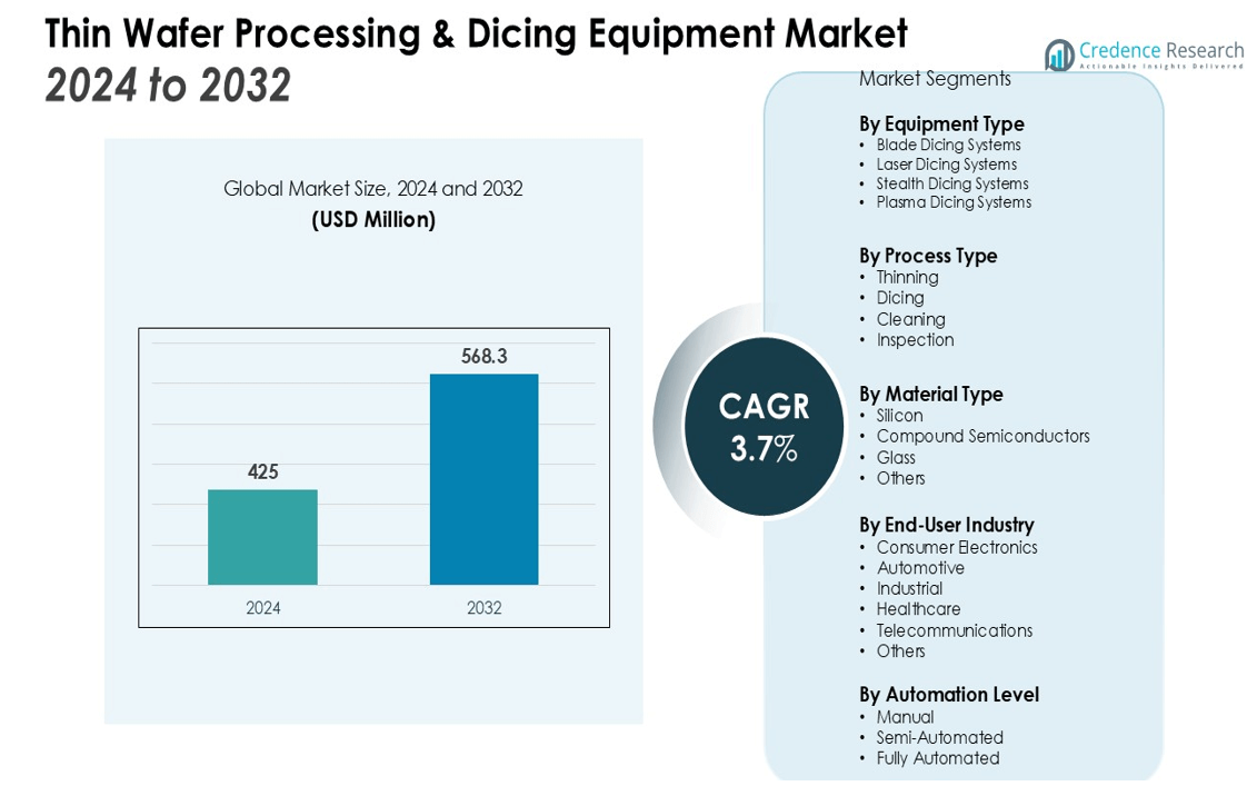
The Thin Wafer Processing & Dicing Equipment Market size was valued at USD 425 million in 2024 and is anticipated to reach USD 568.3 million by 2032, at a CAGR of 3.7% during the forecast period (2024-2032).
| REPORT ATTRIBUTE |
DETAILS |
| Historical Period |
2020-2023 |
| Base Year |
2024 |
| Forecast Period |
2025-2032 |
| Thin Wafer Processing & Dicing Equipment Market Size 2024 |
USD 425 million |
| Thin Wafer Processing & Dicing Equipment Market, CAGR |
3.7% |
| Thin Wafer Processing & Dicing Equipment Market Size 2032 |
USD 568.3 million |
Key market drivers include the surge in demand for consumer electronics, particularly smartphones and wearable devices, which require highly efficient and reliable semiconductor components. The growth of the automotive and industrial IoT sectors, alongside technological advancements in wafer thinning, laser dicing, and stealth dicing methods, further propels market expansion. Additionally, the transition to 5G infrastructure and the proliferation of AI-powered devices are generating new requirements for advanced wafer processing technologies. The growing adoption of 3D integrated circuits and advanced sensor applications is also significantly elevating the need for next-generation dicing and processing solutions.
Regionally, Asia Pacific commands the largest share of the Thin Wafer Processing & Dicing Equipment Market, supported by robust semiconductor manufacturing bases in China, Taiwan, South Korea, and Japan. North America and Europe are also witnessing strong growth, driven by sustained R&D investments and the increasing adoption of advanced packaging technologies.
Access crucial information at unmatched prices!
Request your sample report today & start making informed decisions powered by Credence Research Inc.!
Download Sample
Market Insights:
- The Thin Wafer Processing & Dicing Equipment Market is valued at USD 425 million and projected to reach USD 568.3 million by 2032, with a CAGR of 3.7% during the forecast period.
- Rising demand for miniaturized consumer electronics, including smartphones and wearable devices, drives substantial investments in precise wafer thinning and dicing equipment.
- Automotive and industrial IoT applications create robust demand for thin, high-performance semiconductor components, requiring advanced dicing technologies that ensure safety, durability, and efficiency.
- Advancements in wafer thinning, laser dicing, and stealth dicing methods enable improved yields, reduced material waste, and higher throughput for next-generation semiconductor manufacturing.
- The emergence of 5G, AI-powered devices, and 3D integrated circuits increases requirements for ultra-thin wafer processing solutions, strengthening the market’s role in supporting smart technology ecosystems.
- Complexity in wafer handling and integration challenges overall yield, placing pressure on suppliers to deliver robust, highly specialized equipment that minimizes risks and production costs.
- Asia Pacific leads the market with a 54% share, North America accounts for 23%, and Europe holds 15%, each benefiting from strong industrial bases, R&D investment, and advanced manufacturing practices.
Market Drivers:
Rising Demand for Miniaturized Consumer Electronics
The Thin Wafer Processing & Dicing Equipment Market benefits from the surge in consumer electronics that prioritize thinner, lighter, and more efficient devices. Smartphones, tablets, and wearable electronics require advanced wafer dicing solutions to enable high-density packaging and optimized device performance. Manufacturers invest in equipment that supports precise wafer thinning and dicing to meet the growing expectations for compactness and reliability. It enables electronics brands to deliver innovative features within smaller form factors while maintaining performance standards.
- For instance, PI (Physik Instrumente) provides advanced motion systems for laser dicing with a resolution of 1 nanometer, allowing for highly accurate cuts and minimal material loss.
Growth in Automotive and Industrial IoT Applications
Automotive electronics and industrial IoT applications fuel significant demand in the Thin Wafer Processing & Dicing Equipment Market. The industry shift toward electric vehicles, advanced driver-assistance systems, and smart industrial sensors increases the need for thin, high-performance semiconductor components. Equipment manufacturers respond by developing technologies that ensure wafer integrity and production efficiency. It allows suppliers to cater to stringent requirements in safety, durability, and energy efficiency.
- For instance, Infineon Technologies has pioneered the processing of ultra-thin silicon power wafers just 20 micrometers thick, a quarter of the thickness of a human hair.
Advancements in Wafer Thinning and Dicing Technologies
Continuous innovations in wafer thinning, laser dicing, and stealth dicing methods enhance the capabilities of the Thin Wafer Processing & Dicing Equipment Market. The adoption of advanced dicing technologies results in improved wafer yield and reduced material waste. Equipment providers introduce precision tools that support next-generation semiconductor fabrication. It helps semiconductor manufacturers achieve higher throughput and lower operational costs.
Emergence of 5G, AI, and 3D Integrated Circuits
The deployment of 5G networks and the integration of AI features in devices create new requirements for wafer processing equipment. Manufacturers in the Thin Wafer Processing & Dicing Equipment Market supply solutions that support 3D integrated circuits and sophisticated sensor applications. Evolving end-user demands drive the need for equipment that handles ultra-thin wafers with exceptional accuracy and reliability. It strengthens the market’s role in enabling advanced connectivity and smart technology solutions.
Market Trends:
Adoption of Advanced Dicing and Packaging Technologies
The Thin Wafer Processing & Dicing Equipment Market is witnessing increased adoption of advanced dicing methods such as laser dicing, stealth dicing, and plasma dicing, which offer superior precision and minimal wafer damage. Semiconductor manufacturers focus on enhancing yield and reducing material loss to support the ongoing trend toward miniaturization and higher functionality in electronic devices. The integration of these innovative dicing techniques enables efficient processing of ultra-thin wafers, essential for modern applications such as high-performance memory, logic devices, and sensors. It also supports the evolution of advanced packaging solutions, including 2.5D and 3D integration, to meet the rising requirements for higher density and improved thermal management. Equipment providers respond by launching automated systems that offer greater accuracy, speed, and flexibility for high-volume manufacturing. Companies leverage these technologies to maintain competitive advantages in a fast-evolving market landscape.
- For instance, KLA’s plasma dicing systems can process wafers up to 300mm in diameter and are designed for full automation, supporting overhead track (OHT) and auto-guided vehicles (AGV) for wafer handling in the factory.
Shift Toward Industry 4.0 and Smart Manufacturing Practices
The Thin Wafer Processing & Dicing Equipment Market reflects a broader shift toward Industry 4.0 and the digital transformation of semiconductor manufacturing. Industry participants implement automation, artificial intelligence, and real-time data analytics to optimize wafer processing workflows and reduce operational costs. It enables predictive maintenance, quality assurance, and adaptive control, driving efficiency and consistency in production lines. Manufacturers invest in smart factories that leverage interconnected systems and robotics for scalable, high-precision wafer processing. This trend supports the rapid pace of innovation in sectors such as automotive, consumer electronics, and healthcare. The market is poised to benefit from the continued integration of smart manufacturing practices and the growing demand for connected, data-driven equipment solutions.
- For instance, Intel utilizes 16 production AI models to automatically tag about 2,500 wafers each day, significantly accelerating the detection of manufacturing issues across its facilities.
Market Challenges Analysis:
Complexity of Wafer Handling and Process Integration
The Thin Wafer Processing & Dicing Equipment Market faces significant challenges due to the fragile nature of ultra-thin wafers and the intricacies of integrating multiple advanced processes. Wafer breakage, warping, and alignment errors can impact overall yield and increase production costs. Manufacturers require highly specialized equipment that ensures precise handling and stability throughout the dicing and thinning stages. It places continuous pressure on equipment suppliers to deliver robust, adaptable solutions that minimize risks. The market must address these operational challenges to maintain high standards of reliability and output.
High Capital Investment and Evolving Technology Demands
Entry barriers in the Thin Wafer Processing & Dicing Equipment Market remain high due to the substantial capital investment required for state-of-the-art machinery and ongoing research and development. Rapid advances in device miniaturization and integration demand frequent upgrades and the adoption of new technologies, which can strain budgets for both established players and new entrants. It creates a highly competitive environment where only firms with strong financial and technical resources can sustain long-term growth. Cost pressures and the need for continuous innovation shape strategic decisions across the industry.
Market Opportunities:
Expansion of Applications in Emerging Electronics and Automotive Sectors
The Thin Wafer Processing & Dicing Equipment Market is positioned to capture substantial opportunities in emerging electronics and the expanding automotive industry. Growing demand for advanced driver-assistance systems, electric vehicles, and high-performance consumer devices increases the need for ultra-thin and high-precision semiconductor components. It enables suppliers to deliver specialized equipment that supports new product launches and evolving technology standards. The proliferation of smart devices, IoT applications, and edge computing opens new avenues for market growth. Manufacturers that develop adaptable, high-throughput solutions stand to benefit from rising investments in next-generation electronics production.
Growth Potential in 3D Integration and Advanced Packaging Technologies
The evolution toward 3D integration and advanced packaging presents significant market opportunities for the Thin Wafer Processing & Dicing Equipment Market. Increased adoption of 2.5D and 3D semiconductor architectures in memory, sensors, and logic devices drives demand for precise dicing and handling technologies. It positions equipment suppliers to play a critical role in the future of miniaturized, high-density electronics manufacturing. Companies that invest in R&D and align solutions with customer requirements can secure long-term partnerships and expand their footprint in fast-growing technology segments.
Market Segmentation Analysis:
By Equipment Type
The Thin Wafer Processing & Dicing Equipment Market encompasses blade dicing systems, laser dicing systems, stealth dicing systems, and plasma dicing systems. Blade dicing systems maintain strong usage due to their reliability in traditional semiconductor processes. Laser and stealth dicing systems are expanding their presence, delivering high precision and minimal wafer damage essential for advanced packaging applications. Plasma dicing systems emerge as a leading option for ultra-thin wafer handling, supporting innovations in next-generation device manufacturing. It enables the industry to achieve finer cuts and improved yield in sensitive substrates.
- For instance, Plasma‑Therm Singulator® MOD‑100 and MDS‑300 plasma‑dicing‑on‑tape systems support wafer sizes from 100 mm up to 300 mm in diameter (i.e. 12″ wafers), and are capable of achieving street widths as small as 10 µm or below through their advanced plasma-based etching process.
By Process Type
Segmented by process type, the Thin Wafer Processing & Dicing Equipment Market features thinning, dicing, cleaning, and inspection processes. Thinning and dicing remain at the forefront, driven by the demand for compact, high-density electronic assemblies. Cleaning and inspection equipment play a crucial role in ensuring defect-free output, meeting strict quality requirements across end-use industries. It reinforces production efficiency and helps maintain consistency in final product performance.
- For instance, DISCO Corporation’s TAIKO process, a unique wafer backgrinding method, enhances thin wafer stability by leaving a supportive ring of approximately 3 mm on the wafer’s outer edge.
By Material Type
The market addresses silicon, compound semiconductors, and other specialty materials within its material type segmentation. Silicon continues to dominate, fueled by its foundational role in most electronic and memory devices. Demand for compound semiconductors such as gallium arsenide and silicon carbide grows rapidly, linked to expanding applications in power electronics and optoelectronics. It pushes equipment providers to deliver tailored solutions for diverse wafer characteristics, supporting the evolution of advanced and niche semiconductor technologies.
Segmentations:
By Equipment Type:
- Blade Dicing Systems
- Laser Dicing Systems
- Stealth Dicing Systems
- Plasma Dicing Systems
By Process Type:
- Thinning
- Dicing
- Cleaning
- Inspection
By Material Type:
- Silicon
- Compound Semiconductors
- Glass
- Others
By End-User Industry:
- Consumer Electronics
- Automotive
- Industrial
- Healthcare
- Telecommunications
- Others
By Automation Level:
- Manual
- Semi-Automated
- Fully Automated
By Region:
- North America
- Europe
- Germany
- France
- U.K.
- Italy
- Spain
- Rest of Europe
- Asia Pacific
- China
- Japan
- India
- South Korea
- South-east Asia
- Rest of Asia Pacific
- Latin America
- Brazil
- Argentina
- Rest of Latin America
- Middle East & Africa
- GCC Countries
- South Africa
- Rest of the Middle East and Africa
Regional Analysis:
Asia Pacific: Leadership in Semiconductor Manufacturing and Innovation
Asia Pacific holds a 54% share of the Thin Wafer Processing & Dicing Equipment Market, maintaining its position as the primary hub for production and innovation. The region’s market share reflects the concentration of leading semiconductor manufacturers in China, Taiwan, South Korea, and Japan. Asia Pacific benefits from well-established supply chains, significant investments in R&D, and government initiatives that encourage advanced technology adoption. It drives rapid expansion of wafer fabrication facilities and continuous upgrades to dicing equipment to meet evolving device requirements. The thriving electronics, automotive, and industrial sectors reinforce Asia Pacific’s leadership, consistently attracting multinational equipment suppliers seeking to capitalize on strong demand and growth prospects.
North America: Growth Fueled by Technological Advancements and R&D Focus
North America accounts for 23% of the Thin Wafer Processing & Dicing Equipment Market, supported by its leading role in semiconductor innovation and research. The United States, with its advanced R&D infrastructure and presence of major technology firms, continues to drive next-generation wafer processing solutions. It benefits from ongoing advancements in AI, IoT, and automotive electronics, which require sophisticated dicing technologies. The region’s focus on high-value, precision manufacturing drives sustained investment in equipment and process improvements. Collaborations between academic institutions, technology companies, and equipment manufacturers support a dynamic, forward-looking market environment.
Europe: Emphasis on Advanced Packaging and Sustainability
Europe holds a 15% share of the Thin Wafer Processing & Dicing Equipment Market, positioning itself as a key player in advanced packaging and sustainable manufacturing. Countries such as Germany, France, and the Netherlands prioritize miniaturization, innovation, and adherence to strict quality standards. It leads to strong adoption of efficient wafer thinning and dicing equipment throughout the region. The market benefits from a mix of public and private sector investments and a robust industrial base. Companies operating in Europe often leverage automation and green technologies to address evolving customer needs and maintain competitiveness.
Shape Your Report to Specific Countries or Regions & Enjoy 30% Off!
Key Player Analysis:
- EV Group
- Lam Research Corporation
- DISCO Corporation
- Plasma-Therm
- Tokyo Electron Ltd
- Advanced Dicing Technologies
- SPTS Technologies
- Suzhou Delphi Laser
- Panasonic
- Tokyo Seimitsu
Competitive Analysis:
The Thin Wafer Processing & Dicing Equipment Market features a competitive landscape defined by technological innovation and strategic partnerships. Leading companies include DISCO Corporation, Tokyo Seimitsu Co., Ltd., Synova SA, Kulicke & Soffa, and Plasma-Therm. These firms focus on expanding product portfolios with advanced dicing, laser, and plasma solutions to address the evolving requirements of semiconductor manufacturers. It drives market competition through continuous R&D investment, patent filings, and collaboration with chipmakers. Companies leverage automation, process integration, and precision engineering to deliver superior yield and throughput. New entrants target niche segments with specialized equipment, while established players maintain strong global distribution networks and service capabilities. The competitive dynamics emphasize speed to market, equipment reliability, and alignment with advanced semiconductor production trends.
Recent Developments:
- In May 2025, EV Group announced its hybrid bonding, maskless lithography, and layer transfer solutions would be featured at the Electronic Components and Technology Conference (ECTC) 2025.
- In March 2025, EV Group launched its next-generation GEMINI® automated production wafer bonding system, specifically for 300-mm MEMS manufacturing.
Market Concentration & Characteristics:
The Thin Wafer Processing & Dicing Equipment Market exhibits moderate to high market concentration, with a few key players dominating global sales and technological advancements. It is characterized by a strong emphasis on innovation, high entry barriers due to capital requirements, and rigorous quality standards demanded by semiconductor manufacturers. Leading companies continuously invest in R&D to enhance process precision and efficiency, ensuring alignment with evolving device miniaturization trends. The market prioritizes equipment reliability, customization, and integration with automation systems, while suppliers maintain close partnerships with major semiconductor foundries and electronics producers. This landscape drives a focus on long-term contracts, global service networks, and rapid adoption of advanced technologies.
Report Coverage:
The research report offers an in-depth analysis based on Equipment Type, Process Type, Material Type, End-User Industry, Automation Level and Region. It details leading market players, providing an overview of their business, product offerings, investments, revenue streams, and key applications. Additionally, the report includes insights into the competitive environment, SWOT analysis, current market trends, as well as the primary drivers and constraints. Furthermore, it discusses various factors that have driven market expansion in recent years. The report also explores market dynamics, regulatory scenarios, and technological advancements that are shaping the industry. It assesses the impact of external factors and global economic changes on market growth. Lastly, it provides strategic recommendations for new entrants and established companies to navigate the complexities of the market.
Future Outlook:
- The Thin Wafer Processing & Dicing Equipment Market will see increasing adoption of automation and smart manufacturing technologies to enhance process efficiency and reduce operational costs.
- Advanced dicing solutions such as laser and plasma systems will gain wider acceptance for their ability to support ultra-thin wafer applications and improve product yields.
- Demand for high-precision equipment will intensify as miniaturization and integration trends accelerate in consumer electronics, automotive, and IoT sectors.
- Manufacturers will focus on developing flexible equipment that can handle diverse materials, including silicon, compound semiconductors, and specialty substrates.
- Equipment providers will strengthen partnerships with leading semiconductor foundries and device manufacturers to align with rapidly evolving technology requirements.
- The growth of 5G, AI, and advanced sensor technologies will continue to drive investments in next-generation wafer processing and dicing solutions.
- The market will witness an increase in the adoption of eco-friendly and energy-efficient equipment in response to sustainability goals and regulatory standards.
- Companies will prioritize R&D initiatives to introduce features that ensure higher throughput, improved yield, and lower total cost of ownership.
- Geographic expansion in emerging markets will offer new growth avenues for both established and new entrants.
- Continuous advancements in wafer handling, inspection, and cleaning technologies will support higher production volumes and stricter quality benchmarks across the industry.


