| REPORT ATTRIBUTE |
DETAILS |
| Historical Period |
2020-2023 |
| Base Year |
2024 |
| Forecast Period |
2025-2032 |
| EDA Tools for ASIC Design Market Size 2024 |
USD 13,367.01 million |
| EDA Tools for ASIC Design Market, CAGR |
8.75% |
| EDA Tools for ASIC Design Market Size 2032 |
USD 27,404.61 million |
Market Overview:
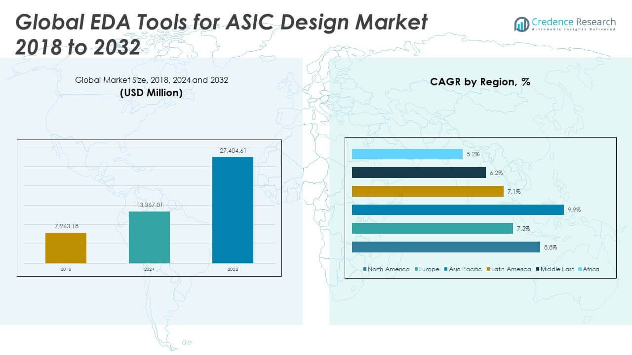
The Global EDA Tools for ASIC Design Market size was valued at USD 7,963.18 million in 2018 to USD 13,367.01 million in 2024 and is anticipated to reach USD 27,404.61 million by 2032, at a CAGR of 8.75% during the forecast period.
The growth of the global EDA tools for ASIC design market is driven by the increasing complexity of integrated circuits and the growing demand for high-performance, low-power semiconductors across emerging technologies. As advanced nodes such as 5nm and below become standard, design intricacies have intensified, prompting the adoption of sophisticated EDA solutions that automate simulation, verification, and layout processes. Additionally, the proliferation of AI, 5G, IoT, and automotive electronics has escalated the need for customized ASICs, further boosting demand for scalable design tools. The integration of AI and machine learning into EDA workflows is also revolutionizing chip design by enhancing design space exploration, accelerating time-to-market, and improving power-performance-area (PPA) outcomes. Furthermore, the shift toward cloud-based EDA platforms enables remote collaboration, elastic compute scalability, and lower infrastructure costs, making advanced design environments accessible to startups and global enterprises alike.
North America leads the global EDA tools for ASIC design market, supported by the presence of key industry players such as Synopsys, Cadence, and Siemens EDA, as well as strong R&D investments and early adoption of AI-enabled semiconductor design tools. The region benefits from a robust ecosystem that includes leading fabless companies, foundries, and cloud infrastructure providers, driving steady demand. In contrast, the Asia-Pacific region is emerging as the fastest-growing market, propelled by rising semiconductor consumption and production in countries like China, Taiwan, South Korea, and India. China’s focus on EDA self-reliance and government-backed initiatives is spurring the development of domestic tools, while Taiwan and South Korea continue to invest in advanced chip design and manufacturing. Europe shows consistent growth, supported by strong automotive and industrial electronics sectors, especially in Germany and France, which are increasingly adopting EDA tools for AI and edge computing applications. Meanwhile, Latin America and the Middle East & Africa are gradually entering the market, encouraged by national digital strategies and expanding electronics design infrastructure.
Market Insights:
- The Global EDA Tools for ASIC Design Market was valued at USD 13,367.01 million in 2024 and is projected to reach USD 27,404.61 million by 2032, growing at a CAGR of 8.75%.
- Increasing IC design complexity and migration to 5nm and smaller nodes are driving the need for advanced EDA tools to manage simulation, verification, and layout.
- Growth in AI, IoT, 5G, and automotive electronics is fueling demand for custom ASICs, boosting reliance on scalable and domain-specific EDA platforms.
- Integration of AI and machine learning into EDA workflows is enabling faster design space exploration, predictive optimization, and reduced time-to-market.
- Cloud-based EDA deployment is gaining traction by enabling real-time collaboration, elastic compute, and accessibility for startups and global teams.
- High costs and vendor lock-in remain barriers for SMEs, requiring more flexible pricing and tool interoperability to expand market participation.
- North America leads the market in revenue share, while Asia Pacific is the fastest-growing region, supported by government-led chip initiatives and rising design capacity.
Access crucial information at unmatched prices!
Request your sample report today & start making informed decisions powered by Credence Research Inc.!
Download Sample
Market Drivers:
Increasing Design Complexity and Miniaturization of Semiconductor Nodes
The Global EDA Tools for ASIC Design Market is primarily driven by the rising complexity in integrated circuit design and the transition to smaller process nodes. The move from 10nm to 5nm and beyond demands precision, tighter control over design parameters, and advanced automation tools. Manual workflows cannot handle the extensive validation, timing analysis, and layout requirements of today’s chip architectures. EDA tools enable engineers to meet shrinking power, performance, and area (PPA) constraints while optimizing for manufacturability. Companies rely on sophisticated design flows to reduce errors and meet time-to-market goals under aggressive development cycles. The shift to multi-die and 3D packaging architectures further increases reliance on EDA solutions.
- For example, Synopsys reports that its AI-driven DSO.ai platform has been deployed in over 270 customer projects, optimizing chip designs for nodes as small as 5nm and 3nm. This platform uses reinforcement learning to autonomously explore design spaces, resulting in productivity boosts of more than 3x, power reductions up to 15%, and significant die size reductions compared to traditional approaches.
Rapid Proliferation of AI, IoT, 5G, and Automotive Electronics
The expansion of high-growth application areas such as artificial intelligence, 5G connectivity, IoT devices, and electric vehicles continues to fuel demand for application-specific integrated circuits. These applications require customized, power-efficient, and high-performance chips tailored to specific workloads. The Global EDA Tools for ASIC Design Market benefits from this trend by offering scalable and efficient design tools that support various architectures and system-on-chip (SoC) configurations. It plays a central role in enabling domain-specific ASIC development that traditional general-purpose processors cannot match. Industries across sectors are prioritizing chip differentiation, increasing dependency on reliable and intelligent EDA ecosystems. The rising use of edge AI and real-time systems also reinforces demand for accurate simulation and verification platforms.
- For example, Keysight’s EDA 2025 software suite incorporates AI and Python-driven automation, reducing RF device modeling time from days to hours and accelerating chiplet interconnect design.
Integration of Artificial Intelligence and Machine Learning into EDA Workflows
Leading EDA vendors are embedding artificial intelligence and machine learning algorithms into their tools to improve design optimization and productivity. AI-enabled platforms help engineers explore larger design spaces, identify optimal configurations, and resolve timing bottlenecks more efficiently. Tools such as Synopsys DSO.ai illustrate how AI is transforming traditional design workflows into more adaptive and intelligent processes. It allows for better PPA outcomes while reducing the number of design iterations. This integration of AI also enhances automated verification, fault prediction, and resource allocation across projects. The Global EDA Tools for ASIC Design Market leverages these technologies to offer faster, more reliable, and resource-efficient design environments.
Transition Toward Cloud-Based EDA Platforms and Collaborative Design Models
The adoption of cloud computing models has introduced flexibility, scalability, and accessibility to the EDA tool landscape. Cloud-based platforms support real-time collaboration among geographically distributed teams, enabling faster prototyping and seamless iteration. It reduces capital expenditure on local infrastructure while providing access to high-performance computing resources. The Global EDA Tools for ASIC Design Market is evolving toward cloud-first deployment models to support agile development cycles and growing demand from startups and SMEs. These platforms also simplify license management and integration with third-party IP and verification libraries. This shift is driving broader participation in ASIC design and fostering innovation in emerging markets.
Market Trends:
Growing Focus on Hardware–Software Co-Design and Co-Verification Strategies
The convergence of hardware and software development cycles is emerging as a prominent trend within the Global EDA Tools for ASIC Design Market. Developers now prioritize parallel design flows that align hardware specifications with early software integration. It supports earlier bug detection, improved system performance, and faster prototyping. Tools offering simulation of embedded software alongside hardware design allow better synchronization between firmware and chip functionality. This approach is gaining traction in automotive and AI sectors where real-time system responsiveness is critical. Companies investing in co-design and co-verification strategies are better equipped to meet functional safety and time-to-market targets.
Rising Importance of Open-Source EDA Platforms and Interoperability
The industry has seen a noticeable shift toward open-source EDA frameworks that promote transparency, flexibility, and community-driven innovation. Projects like OpenROAD and collaborative university-led initiatives are enabling cost-effective alternatives to proprietary tools. The Global EDA Tools for ASIC Design Market is responding to this trend by improving tool interoperability and supporting open standards. It encourages modular toolchains, allowing engineers to choose best-in-class solutions across vendors without locking into a single ecosystem. This openness drives efficiency in design workflows and expands access to smaller companies and academic institutions. Open EDA ecosystems also accelerate innovation through shared development and validation.
- For instance, the OpenROAD Projectis a leading open-source EDA initiative, boasting over 120 active GitHub contributors and more than 600 chip tape-outs at process nodes from 180nm down to 12nm since its inception. OpenROAD’s fully open RTL-to-GDSII flow integrates with tools like Yosys and TritonRoute, enabling academic and startup teams to complete complex ASIC designs without proprietary licenses.
Expanding Role of Digital Twin Technology in ASIC Design Validation
Digital twin adoption is reshaping how designers simulate and validate complex ASIC architectures before committing to physical prototypes. Creating a digital replica of the entire system enables real-time testing under diverse operating conditions. It helps identify design flaws, thermal inefficiencies, and performance bottlenecks in early development stages. The Global EDA Tools for ASIC Design Market is incorporating digital twin models to improve functional and structural validation accuracy. It supports scenario-based testing and design tuning based on real-world data. This approach reduces late-stage redesigns and improves confidence in the final silicon output.
- For example, Siemens Digital Industries Softwarehas embedded advanced digital twin capabilities into its Xcelerator portfolio, including Teamcenter and MindSphere. These tools allow the creation of comprehensive virtual representations of chips and systems, supporting real-time scenario-based testing and validation.
Emphasis on Security-Centric Design Workflows and Trusted IP Integration
Security is becoming a core design consideration in ASIC development due to growing threats targeting chip-level vulnerabilities. Design teams are embedding security features such as hardware roots of trust, secure boot, and cryptographic engines directly into ASICs. The Global EDA Tools for ASIC Design Market is witnessing increased integration of threat modeling, secure logic simulation, and IP provenance verification into design workflows. It supports compliance with standards like ISO/SAE 21434 and NIST guidelines. Trusted IP sourcing and end-to-end validation are now essential for industries handling sensitive data or operating in regulated environments. Security-driven design is no longer optional but a foundational market expectation.
Market Challenges Analysis:
High Cost of EDA Tools and Limited Accessibility for Emerging Enterprises
The high licensing and infrastructure costs associated with advanced EDA tools continue to challenge broader market adoption. Small and medium-sized enterprises often struggle to access high-end ASIC design platforms due to steep upfront investments, recurring fees, and specialized hardware requirements. The Global EDA Tools for ASIC Design Market must address this cost barrier to ensure inclusivity across all levels of the design ecosystem. While cloud-based deployment models have lowered some financial entry points, integration and customization expenses remain considerable for new entrants. It creates a gap between established players and smaller innovators, potentially slowing the pace of decentralized design innovation. Vendor lock-in also exacerbates cost challenges by limiting flexibility in toolchain choices.
Talent Shortage and Complexity in Multi-Domain Design Environments
The increasing complexity of ASIC architectures requires highly skilled professionals capable of navigating multi-domain challenges involving logic, analog, RF, and embedded software integration. A global shortage of semiconductor design engineers limits the scalability of advanced projects, especially in regions where engineering talent pipelines remain underdeveloped. The Global EDA Tools for ASIC Design Market faces pressure to invest in user-friendly platforms and enhanced automation to bridge knowledge gaps. It must support workflows that enable faster onboarding and reduce dependency on niche expertise. Coordination between hardware and software teams also remains a challenge in managing verification, debugging, and iterative optimization across large, distributed teams. Training and upskilling efforts are essential to meet the growing technical demands of next-generation chip design.
Market Opportunities:
Expansion into Emerging Markets and Government-Backed Semiconductor Initiatives
Developing economies are rapidly expanding their semiconductor capabilities, presenting significant growth prospects for the Global EDA Tools for ASIC Design Market. Countries such as India, Vietnam, and Brazil are launching national programs to boost domestic chip design and manufacturing. It creates new demand for accessible, localized EDA solutions tailored to regional infrastructure and educational needs. Government funding, tax incentives, and public–private partnerships are accelerating adoption among startups and universities. Vendors that tailor offerings to these markets through cost-effective licensing and training programs can establish early market leadership. This expansion aligns with global efforts to diversify semiconductor supply chains and reduce dependency on mature regions.
Growth Potential in AI-Driven Automation and IP Marketplace Integration
Automation powered by artificial intelligence unlocks opportunities for faster design iterations, predictive optimization, and intelligent verification. The Global EDA Tools for ASIC Design Market can benefit from embedding AI models that assist engineers in debugging, performance tuning, and resource allocation. Another emerging opportunity lies in integrating online IP marketplaces directly into EDA platforms. It enables seamless access to pre-verified blocks, accelerating development while maintaining quality. These capabilities can reshape workflows and create new revenue streams through on-demand IP licensing. It positions EDA providers as enablers of ecosystem-level innovation beyond tool delivery.
Market Segmentation Analysis:
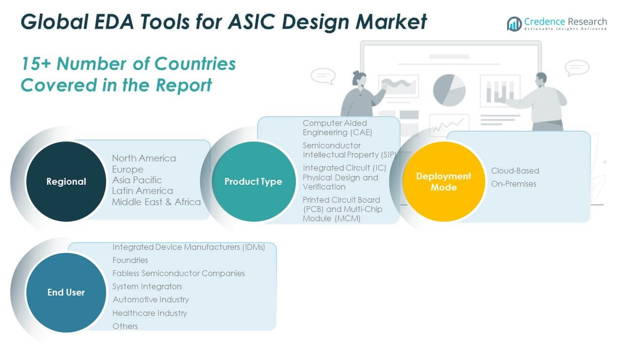
The Global EDA Tools for ASIC Design Market is segmented by product type, deployment mode, and end user, each reflecting distinct demand drivers and use cases.
By product types, Computer Aided Engineering (CAE) holds a substantial share due to its critical role in functional verification and performance analysis. Semiconductor Intellectual Property (SIP) continues to grow with the rising need for reusable and pre-verified design blocks. IC Physical Design and Verification is gaining traction with the shift toward advanced nodes. Printed Circuit Board (PCB) and Multi-Chip Module (MCM) tools support packaging innovation and integration.
- For example, Synopsysintroduced the Fusion Compiler™, a leading-edge RTL-to-GDSII tool suite used by Samsung Foundry to tape out 3nm Gate-All-Around (GAA) chips.
By deployment mode, cloud-based platforms are witnessing faster growth due to their scalability and collaborative capabilities, while on-premises solutions remain relevant in high-security or legacy design environments. The Global EDA Tools for ASIC Design Market supports both to address varying infrastructure needs.
- For instance, Google’s collaboration with Siemens EDA launched IC design-in-the-cloud solutions via Google Cloud, allowing partners to run entire ASIC flows without local infrastructure.
By end users, fabless semiconductor companies lead in tool adoption due to their focus on complex SoC designs and outsourcing models. Integrated Device Manufacturers (IDMs) and foundries continue to invest in in-house EDA tools for vertical integration. System integrators, automotive, and healthcare sectors are increasing adoption for customized ASIC development tailored to performance and reliability.
Segmentation:
By Product Type:
- Computer Aided Engineering (CAE)
- Semiconductor Intellectual Property (SIP)
- Integrated Circuit (IC) Physical Design and Verification
- Printed Circuit Board (PCB) and Multi-Chip Module (MCM)
By Deployment Mode:
By End User:
- Integrated Device Manufacturers (IDMs)
- Foundries
- Fabless Semiconductor Companies
- System Integrators
- Automotive Industry
- Healthcare Industry
- Others
By Region:
- North America
- Europe
- Germany
- France
- U.K.
- Italy
- Spain
- Rest of Europe
- Asia Pacific
- China
- Japan
- India
- South Korea
- South-east Asia
- Rest of Asia Pacific
- Latin America
- Brazil
- Argentina
- Rest of Latin America
- Middle East & Africa
- GCC Countries
- South Africa
- Rest of the Middle East and Africa
Regional Analysis:
North America
The North America EDA Tools for ASIC Design Market size was valued at USD 3,331.31 million in 2018 to USD 5,531.34 million in 2024 and is anticipated to reach USD 11,373.05 million by 2032, at a CAGR of 8.8% during the forecast period. North America holds the largest share of the Global EDA Tools for ASIC Design Market, accounting for approximately 34% in 2024. The region benefits from a well-established semiconductor ecosystem with leading companies such as Synopsys, Cadence Design Systems, and Siemens EDA headquartered in the U.S. It is also supported by high R&D investments, robust academic partnerships, and early adoption of AI-based and cloud-enabled design platforms. The market continues to expand with the growing presence of fabless semiconductor firms and deep-tech startups focused on AI, autonomous vehicles, and high-performance computing. Government funding for advanced semiconductor research and export control policies also influence EDA tool innovation and adoption across the region.
Europe
The Europe EDA Tools for ASIC Design Market size was valued at USD 1,571.45 million in 2018 to USD 2,501.14 million in 2024 and is anticipated to reach USD 4,689.28 million by 2032, at a CAGR of 7.5% during the forecast period. Europe commands around 15% of the Global EDA Tools for ASIC Design Market in 2024, driven by a focus on automotive electronics, industrial automation, and telecommunications. Countries such as Germany, France, and the Netherlands support semiconductor innovation through public-private R&D initiatives and strategic funding. It plays a critical role in delivering ASIC designs for energy-efficient mobility, sensor systems, and industrial IoT applications. The region also invests in developing homegrown EDA capabilities to strengthen its semiconductor sovereignty goals. Rising interest in secure chip design and edge AI solutions provides new momentum to the European EDA market.
Asia Pacific
The Asia Pacific EDA Tools for ASIC Design Market size was valued at USD 2,368.65 million in 2018 to USD 4,191.69 million in 2024 and is anticipated to reach USD 9,351.14 million by 2032, at a CAGR of 9.9% during the forecast period. Asia Pacific holds a 26% share of the Global EDA Tools for ASIC Design Market in 2024, with strong momentum across China, Taiwan, South Korea, and India. The region benefits from growing chip design talent, government-backed semiconductor programs, and heavy investments in AI, 5G, and consumer electronics. China is prioritizing domestic EDA development to reduce reliance on foreign vendors, supporting firms like Empyrean and Primarius. It remains the fastest-growing regional market, driven by increasing demand for localized and vertically integrated chip design. Asia Pacific is expected to lead future ASIC innovation due to its large-scale manufacturing base and expanding digital economy.
Latin America
The Latin America EDA Tools for ASIC Design Market size was valued at USD 376.10 million in 2018 to USD 623.47 million in 2024 and is anticipated to reach USD 1,131.34 million by 2032, at a CAGR of 7.1% during the forecast period. Latin America holds approximately 4% share of the Global EDA Tools for ASIC Design Market in 2024. The region shows potential due to growing interest in electronics manufacturing, embedded systems, and IoT innovation. Brazil and Mexico lead in semiconductor design activities supported by university research centers and public funding for digital infrastructure. It faces challenges such as limited local tool availability and reliance on global vendors for advanced design solutions. However, increasing cloud adoption and government-led tech initiatives create opportunities for broader EDA tool usage across startups and academic institutions.
Middle East
The Middle East EDA Tools for ASIC Design Market size was valued at USD 208.87 million in 2018 to USD 318.45 million in 2024 and is anticipated to reach USD 543.26 million by 2032, at a CAGR of 6.2% during the forecast period. The Middle East contributes 2% to the Global EDA Tools for ASIC Design Market in 2024. It is witnessing moderate growth as countries like the UAE and Saudi Arabia invest in digital transformation and national semiconductor programs. Government initiatives focused on building local technology capabilities are creating demand for chip design tools and training. It also benefits from regional interest in smart infrastructure, defense electronics, and AI adoption. However, limited domestic tool development and workforce constraints may slow market maturity without sustained investment and international collaboration.
Africa
The Africa EDA Tools for ASIC Design Market size was valued at USD 106.79 million in 2018 to USD 200.92 million in 2024 and is anticipated to reach USD 316.55 million by 2032, at a CAGR of 5.2% during the forecast period. Africa holds just under 1.5% of the Global EDA Tools for ASIC Design Market in 2024. The market remains nascent due to low levels of semiconductor infrastructure and limited access to advanced design tools. South Africa leads in regional academic research and innovation ecosystems, while other nations are exploring digital economy strategies. It presents long-term potential through education partnerships and cloud-based access to global EDA platforms. Expansion of local design centers and training programs will be critical to future growth. Broader mobile technology penetration and digital health initiatives may drive demand for customized ASICs over the next decade.
Shape Your Report to Specific Countries or Regions & Enjoy 30% Off!
Key Player Analysis:
- Synopsys
- Cadence Design Systems
- Siemens EDA (Mentor Graphics)
- Ansys
- Keysight Technologies
- Altium Limited
- Zuken
- Silvaco
- Altair
- Empyrean Technology
Competitive Analysis:
The Global EDA Tools for ASIC Design Market features a concentrated competitive landscape dominated by a few key players, including Synopsys, Cadence Design Systems, and Siemens EDA. These companies maintain strong market positions through extensive product portfolios, continuous R&D investment, and integration of AI and machine learning into design workflows. It also includes emerging players such as Empyrean Technology and Primarius, which are gaining traction in Asia through localized tool development and government support. Strategic collaborations with foundries and cloud providers strengthen the value proposition of leading vendors. The market is witnessing increased competition driven by the demand for faster, more efficient, and scalable ASIC design solutions. Vendors focus on expanding cloud-based offerings, enhancing IP portfolios, and enabling hardware–software co-design to differentiate their platforms. Competitive intensity is expected to rise as regional players innovate and open-source tools gain momentum in academic and startup environments.
Recent Developments:
- In June 2025, Siemens EDA unveiled an AI-enhanced toolset for the EDA design flow at the Design Automation Conference. This new system introduces generative and agentic AI capabilities tailored for semiconductor and PCB design, offering secure, customizable integration across the entire workflow. Siemens aims to revolutionize design team productivity and accelerate time to market by embedding AI deeply into EDA processes.
- In May 2025, Zuken launched the 2025 version of its flagship PCB design suite, CR-8000, featuring AI-enhanced support for high-speed, high-density PCB design. The new release introduces intelligent schematic automation, delay-aware routing, and AI-assisted features that streamline design tasks, ensuring timing compliance and first-pass success in advanced PCB projects.
- In March 2025, Silvaco expanded its product offering through the acquisition of Cadence’s Process Proximity Compensation (PPC) product line. This acquisition enhances Silvaco’s EDA and TCAD portfolio, enabling deeper customer collaborations and strengthening its position in high-growth sectors such as AI, photonics, and IoT. The integration of PPC is expected to drive further growth and value for Silvaco’s customers in 2025.
- In January 2025, Altium completed the acquisition of Part Analytics, an AI-powered supply chain management platform. This strategic move will integrate advanced component and parts management capabilities into Altium’s cloud-based collaboration platform, Altium 365, enhancing support for electronics supply chain and procurement processes and furthering Altium’s vision for a connected electronics value chain.
Market Concentration & Characteristics:
The Global EDA Tools for ASIC Design Market exhibits a high level of market concentration, with a small number of established players controlling a significant share of global revenues. It is characterized by high entry barriers due to the complexity of tool development, long product validation cycles, and the need for deep domain expertise. The market demands continuous innovation, driven by rapid advances in semiconductor technologies and the need for integrated, scalable design solutions. Vendor differentiation hinges on the ability to support advanced nodes, AI-enhanced automation, and seamless cloud deployment. It remains highly specialized, with strong customer lock-in due to proprietary design flows and ecosystem integration. While dominant firms maintain their leadership through innovation and partnerships, open-source initiatives and regional tool development are slowly introducing competitive alternatives.
Report Coverage:
The research report offers an in-depth analysis based on product type, deployment mode, and end user. It details leading market players, providing an overview of their business, product offerings, investments, revenue streams, and key applications. Additionally, the report includes insights into the competitive environment, SWOT analysis, current market trends, as well as the primary drivers and constraints. Furthermore, it discusses various factors that have driven market expansion in recent years. The report also explores market dynamics, regulatory scenarios, and technological advancements that are shaping the industry. It assesses the impact of external factors and global economic changes on market growth. Lastly, it provides strategic recommendations for new entrants and established companies to navigate the complexities of the market.
Future Outlook:
- Demand for advanced-node support will accelerate as chipmakers adopt 3nm and below for next-generation ASICs.
- AI-driven automation will enhance design optimization, reducing development cycles and engineering effort.
- Cloud-based EDA platforms will gain broader adoption, enabling real-time collaboration and scalable compute access.
- Hardware–software co-design will become essential, aligning chip functionality with system-level performance needs.
- Open-source EDA tools will expand in academic and startup environments, challenging proprietary solutions in niche segments.
- Emerging markets will contribute significantly to growth through national semiconductor initiatives and design ecosystem development.
- Cybersecurity-focused design tools will gain prominence due to rising threats and stricter compliance requirements.
- IP marketplace integration within EDA platforms will streamline access to reusable components, shortening time-to-market.
- Ecosystem partnerships between EDA vendors, foundries, and cloud providers will shape competitive dynamics.
- Talent development and upskilling programs will become critical to addressing the global shortage of ASIC design professionals.


