| REPORT ATTRIBUTE |
DETAILS |
| Historical Period |
2020-2023 |
| Base Year |
2024 |
| Forecast Period |
2025-2032 |
| Temporary Wafer Bonding and Debonding System Market Size 2024 |
USD 278.29 million |
| Temporary Wafer Bonding and Debonding System Market, CAGR |
6.70% |
| Temporary Wafer Bonding and Debonding System Market Size 2032 |
467.53 million |
Market Overview:
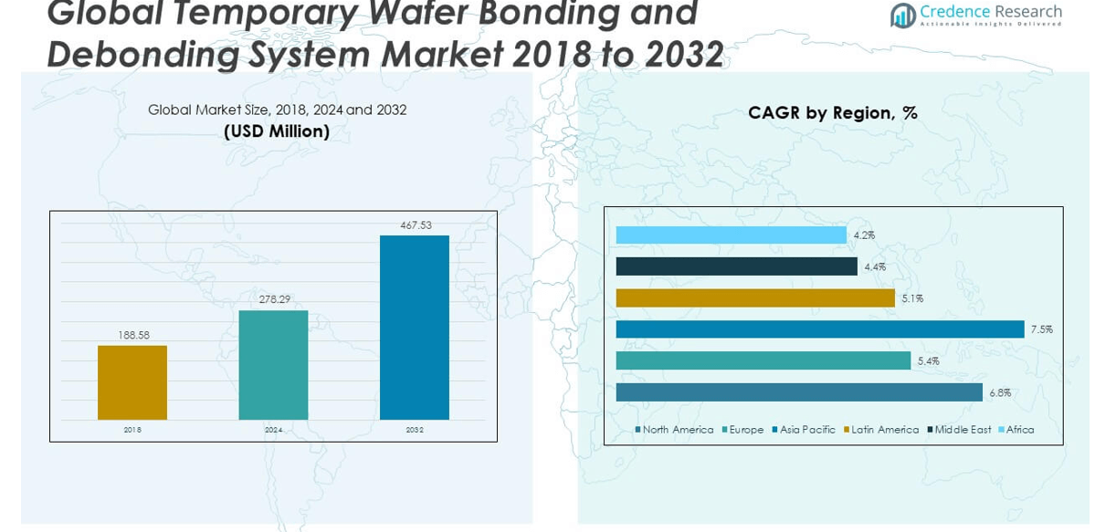
The Global Temporary Wafer Bonding and Debonding System Market size was valued at USD 188.58 million in 2018 to USD 278.29 million in 2024 and is anticipated to reach USD 467.53 million by 2032, at a CAGR of 6.70% during the forecast period.
The rapid advancement of semiconductor packaging technologies is a major driver of the Temporary Wafer Bonding and Debonding System Market. With growing demand for compact, high-performance electronic devices, manufacturers are moving toward 2.5D and 3D integration, chip stacking, and system-in-package (SiP) configurations—all of which require precise temporary bonding for alignment and mechanical support. Additionally, the proliferation of consumer electronics, automotive electronics (especially for ADAS and EVs), and connected devices has spurred significant investment in wafer-level processing. Innovations in debonding techniques, such as laser-based and zone-controlled thermal systems, are further optimizing cycle times and reducing contamination risks, thus increasing the attractiveness of these systems. Moreover, government-backed initiatives in key semiconductor hubs, including the U.S. CHIPS Act and China’s “Made in China 2025” strategy, are accelerating local fabrication capabilities and boosting capital expenditures on advanced wafer processing tools.
Asia Pacific dominates the global temporary wafer bonding and debonding system market, accounting for the largest share due to the concentration of major semiconductor foundries and OSAT (outsourced semiconductor assembly and test) players in countries such as Taiwan, China, South Korea, and Japan. The region’s stronghold is reinforced by strategic government investments, increasing domestic chip demand, and large-scale R&D in packaging innovation. North America follows as a key revenue contributor, driven by a strong presence of leading semiconductor equipment manufacturers, advanced research infrastructure, and federal funding programs to restore semiconductor manufacturing independence. Europe also represents a significant portion of the market, particularly in Germany, France, and the Netherlands, where industrial electronics and automotive sectors fuel the adoption of wafer-level packaging technologies. Meanwhile, the markets in Latin America and the Middle East & Africa are in earlier stages of development, with incremental growth expected through partnerships, technology transfers, and selective semiconductor investments.
Market Insights:
- The market size grew from USD 188.58 million in 2018 to USD 278.29 million in 2024 and is projected to reach USD 467.53 million by 2032, registering a CAGR of 6.70%.
- Advanced packaging trends like 2.5D/3D integration and system-in-package (SiP) are major growth drivers, requiring precise bonding and debonding solutions for ultrathin wafers.
- Rising use of MEMS and power devices in automotive and industrial sectors is expanding demand for robust wafer bonding equipment with material versatility.
- Technological innovations such as laser and zone-controlled thermal debonding are improving yield, reducing cycle times, and broadening application scope.
- Government-backed initiatives like the U.S. CHIPS Act and China’s manufacturing policies are fueling investments in wafer-level processing infrastructure.
- High capital costs and complex integration requirements remain key challenges, particularly for small and mid-sized semiconductor manufacturers.
- Asia Pacific leads the global market due to the presence of major foundries, while North America and Europe follow with strong R&D and semiconductor policy support.
Access crucial information at unmatched prices!
Request your sample report today & start making informed decisions powered by Credence Research Inc.!
Download Sample
Market Drivers:
Rising Demand for Advanced Packaging Technologies Fuels Equipment Adoption
The Global Temporary Wafer Bonding and Debonding System Market is experiencing strong growth due to the increasing demand for advanced semiconductor packaging methods such as 2.5D/3D integration, system-in-package (SiP), and fan-out wafer-level packaging (FOWLP). These approaches require precise wafer handling and temporary bonding solutions to support ultrathin wafers during processing. Manufacturers rely on these systems to maintain alignment and structural integrity throughout the fabrication cycle. The move toward high-performance, compact devices in smartphones, tablets, and wearables is accelerating the adoption of wafer-level packaging, thereby boosting the need for reliable bonding and debonding equipment. Temporary bonding enables backside processing, which is essential for integrating more functionality in smaller footprints. This growing reliance on miniaturized, multifunctional chips is expanding the market’s equipment base.
- For example, EV Group (EVG)introduced its EVG®850 DB automated debonding system, which supports wafer sizes up to 300 mm and achieves alignment accuracy better than ±1 μm, a critical metric for 2.5D/3D integration and FOWLP processes. SÜSS MicroTec reports its XBC300 Gen2 system can handle ultrathin wafers down to 50 μm thickness, maintaining structural integrity during high-volume manufacturing.
Increasing Integration of MEMS and Power Devices Elevates Equipment Demand
MEMS and power semiconductor devices are seeing higher integration in consumer and industrial electronics, driving the need for temporary wafer bonding systems. These devices often require complex manufacturing steps such as deep etching and thinning, which depend on strong mechanical support during processing. It supports the production of MEMS microphones, sensors, RF filters, and power ICs used in automotive and industrial applications. The Global Temporary Wafer Bonding and Debonding System Market benefits from this demand, as it enables high-yield manufacturing of delicate structures. Power devices such as IGBTs and SiC-based components also benefit from temporary bonding in high-temperature fabrication processes. Equipment vendors are responding with solutions that offer compatibility with a wide range of materials and wafer sizes.
Technological Innovations in Bonding Materials and Debonding Methods Expand Use Cases
Advancements in bonding adhesives, laser debonding systems, and thermal zone-controlled techniques are widening the range of applications for temporary wafer bonding equipment. These innovations enable cleaner separation of wafers, minimal residue, and compatibility with a broader set of substrate materials, including glass and compound semiconductors. The market is evolving to meet the needs of high-volume manufacturers by offering automation-ready systems with integrated process control. It supports tight process tolerances and increases yield in complex, multi-step packaging flows. Improved debonding accuracy also reduces damage to wafers and devices during separation. These innovations are making the systems indispensable for next-generation semiconductor production lines.
- For instance, Brewer Science has published data on its ZoneBOND® technology, which utilizes a thermoplastic adhesive that allows for controlled debonding at temperatures below 100°C, reducing wafer warpage and contamination.
Government Incentives and Supply Chain Resilience Drive Capital Investments
National strategies supporting semiconductor independence and localized manufacturing are creating favorable conditions for market growth. Government incentives such as the CHIPS and Science Act in the U.S. and similar programs in Europe and Asia are encouraging fabs to invest in advanced processing tools. The Global Temporary Wafer Bonding and Debonding System Market is gaining from this trend, as new fabs incorporate the latest equipment into their infrastructure. Companies are prioritizing process resilience and cost control, which increases the demand for modular, flexible bonding solutions. Supply chain vulnerabilities exposed during global disruptions have further accelerated the shift toward localized, high-precision manufacturing tools. These factors are contributing to increased capital expenditure in wafer processing equipment.
Market Trends:
Growing Focus on Heterogeneous Integration is Reshaping Equipment Requirements
The increasing adoption of heterogeneous integration is influencing design and process flows across advanced semiconductor packaging lines. Instead of traditional monolithic designs, manufacturers are combining multiple chiplets and components onto a single package. This trend demands greater flexibility and precision in temporary bonding and debonding systems to accommodate varied materials, thicknesses, and form factors. The Global Temporary Wafer Bonding and Debonding System Market is adapting to support hybrid structures that include logic, memory, RF, and sensor elements on a unified substrate. Equipment vendors are optimizing process compatibility with different thermal expansion coefficients and surface chemistries. It is enabling efficient handling of dissimilar wafers and improving yield in complex 3D assembly environments.
Rising Use of Transparent and Non-Silicon Substrates Expands Material Scope
Emerging applications in optoelectronics and advanced photonics are driving the use of transparent materials such as glass and sapphire in wafer processing. These substrates pose new challenges for temporary bonding, including thermal stability, chemical compatibility, and optical transmission needs. Manufacturers require bonding materials and debonding systems that avoid damage while maintaining alignment and surface quality. The Global Temporary Wafer Bonding and Debonding System Market is witnessing a shift in demand toward equipment capable of handling non-silicon substrates without process degradation. Tool manufacturers are developing specialized handling modules, adaptive clamps, and new adhesive chemistries to address these material-specific challenges. It is expanding the market’s reach into niche sectors that require non-traditional wafers.
- For instance, Resonac and PulseForgehave advanced photonic debonding technology specifically for transparent substrates such as glass carriers. Their solution leverages high-intensity pulsed light and light-absorbing glass carriers, enabling clean, low-stress separation of device wafers as thin as 20 µm from temporary carriers.
Integration of Artificial Intelligence and Data Analytics Enhances Process Control
The semiconductor industry’s increasing reliance on real-time data and predictive analytics is influencing the evolution of bonding and debonding tools. Equipment manufacturers are embedding AI and machine learning algorithms to monitor parameters such as alignment precision, temperature control, and force application during bonding. These enhancements improve tool accuracy, reduce downtime, and enable predictive maintenance. The Global Temporary Wafer Bonding and Debonding System Market is embracing smart systems that optimize cycle time and reduce human error in high-mix, high-volume production environments. It is becoming more common to see tools with advanced software interfaces and adaptive process tuning features. This trend supports greater process repeatability and tighter control over quality assurance in next-generation fabs.
Miniaturization in Biomedical Devices and Sensors Drives New Application Areas
The miniaturization of biomedical implants, diagnostics, and wearable sensors is opening up new application areas for wafer bonding and debonding systems. These medical components often require high-precision microfabrication processes, which depend on thin wafer handling and stress-free debonding. The Global Temporary Wafer Bonding and Debonding System Market is finding new opportunities in the medical device sector, where regulatory standards and product customization demand robust, clean processing tools. Equipment manufacturers are responding by offering systems tailored for small-batch production with medical-grade bonding materials. It is creating demand for compact, contamination-free, and biocompatible solutions that meet both performance and compliance requirements. This expansion into healthcare is broadening the market’s end-user base beyond traditional electronics.
- For example, AI Technology, Inc.’s WPA-UVR-270 film enables the safe processing of ultra-thin wafers at temperatures up to 270°C, which is critical for manufacturing miniaturized medical devices. After processing, the film can be cleanly peeled away using UV light, leaving no residue on the wafer surface. This clean release process maintains the high level of cleanliness and biocompatibility required for medical implants and sensors, and helps prevent damage to delicate microstructures.
Market Challenges Analysis:
High Equipment Costs and Complex Integration Limit Accessibility for Small Manufacturers
The high capital investment required for temporary wafer bonding and debonding systems poses a significant barrier, particularly for small and mid-sized semiconductor manufacturers. These systems involve advanced technologies, including precision thermal controls, laser debonding, and high-grade adhesives, which contribute to their elevated cost. The Global Temporary Wafer Bonding and Debonding System Market faces challenges in expanding adoption across less capital-intensive operations due to these high entry costs. Integrating such equipment into existing production lines also demands specialized technical expertise, process revalidation, and infrastructure upgrades. It places added pressure on companies to justify return on investment, especially when handling low production volumes. The complexity of customization for diverse wafer materials and sizes further limits operational flexibility for smaller fabs.
Material Compatibility and Yield Losses Create Process Uncertainties
Ensuring reliable bonding and clean debonding across a wide range of materials remains a technical challenge. Temporary bonding materials must offer high adhesion strength during processing while enabling residue-free separation during debonding, a balance that is difficult to achieve consistently. The Global Temporary Wafer Bonding and Debonding System Market must address frequent yield losses caused by delamination, wafer breakage, or surface contamination. It often requires intensive testing to fine-tune parameters for each new substrate or layer configuration. Any variability in temperature, pressure, or alignment can lead to damage, increasing scrap rates and reducing production efficiency. These risks make manufacturers cautious in fully scaling up bonding/debonding steps for new or experimental device architectures.
Market Opportunities:
Expansion of Advanced Packaging Facilities in Emerging Economies Offers Growth Potential
The growing investment in semiconductor fabrication and advanced packaging facilities in emerging economies such as India, Vietnam, and Malaysia is creating new demand for wafer processing tools. Government incentives and public-private partnerships are encouraging local production and infrastructure development, opening opportunities for equipment suppliers. The Global Temporary Wafer Bonding and Debonding System Market stands to benefit as new fabs seek to incorporate cutting-edge process technologies from the outset. It presents a chance for vendors to offer cost-effective, scalable solutions tailored for developing regions. The rising need for local semiconductor supply chains also supports regional equipment adoption. Companies that can deliver adaptable and training-friendly systems will gain a competitive advantage.
Rising Demand in Photonics, AR/VR, and Compound Semiconductors Expands Application Scope
Emerging applications in photonics, augmented reality/virtual reality devices, and compound semiconductors are driving the need for highly specialized bonding and debonding processes. These technologies often use non-traditional substrates and require ultra-clean processing conditions. The Global Temporary Wafer Bonding and Debonding System Market has an opportunity to expand into these high-value segments by developing tools compatible with sapphire, GaN, and glass wafers. It can support innovation in consumer electronics, defense, and quantum computing sectors. Customization capabilities and material versatility will play a crucial role in addressing this evolving demand. This diversification of end-user industries strengthens long-term market growth prospects.
Market Segmentation Analysis:
The Global Temporary Wafer Bonding and Debonding System Market is segmented by type, application, technology, and end user, each reflecting distinct growth trajectories.
By type, the market includes temporary bonding materials, bonding equipment, and debonding equipment. Temporary bonding equipment leads due to increasing adoption in high-precision packaging processes, while demand for advanced debonding tools is growing with the rise of ultrathin wafers and 3D structures.
- For example, EV Group’s (EVG) GEMINI® FB XT automated fusion bonding system is a leading example of high-precision temporary bonding equipment. This tool is widely adopted for advanced packaging, enabling die-to-wafer and wafer-to-wafer bonding with sub-micron alignment accuracy.
By application, the market spans 3D IC, MEMS, LED, power devices, and others. 3D IC and MEMS dominate the segment due to their critical role in advanced semiconductor packaging and sensor integration. The LED and power device segments are also expanding, driven by energy-efficient lighting and electric vehicle applications.
By technology, the market includes room temperature debonding, laser debonding, chemical debonding, thermal slide debonding, and others. Laser debonding holds the largest share due to its clean separation and high process control. Room temperature and chemical methods are gaining traction for sensitive substrate handling.
- For example, Brewer Science’s chemical release materials allow for controlled debonding by dissolving the adhesive layer with specific solvents, supporting applications that require gentle handling of ultra-thin and fragile wafers.
By end user, the market serves semiconductor and electronics, automotive, healthcare, and others. Semiconductor and electronics companies account for the largest share of demand. The Global Temporary Wafer Bonding and Debonding System Market also sees growing use in automotive and healthcare sectors, where compact, high-reliability devices are essential.
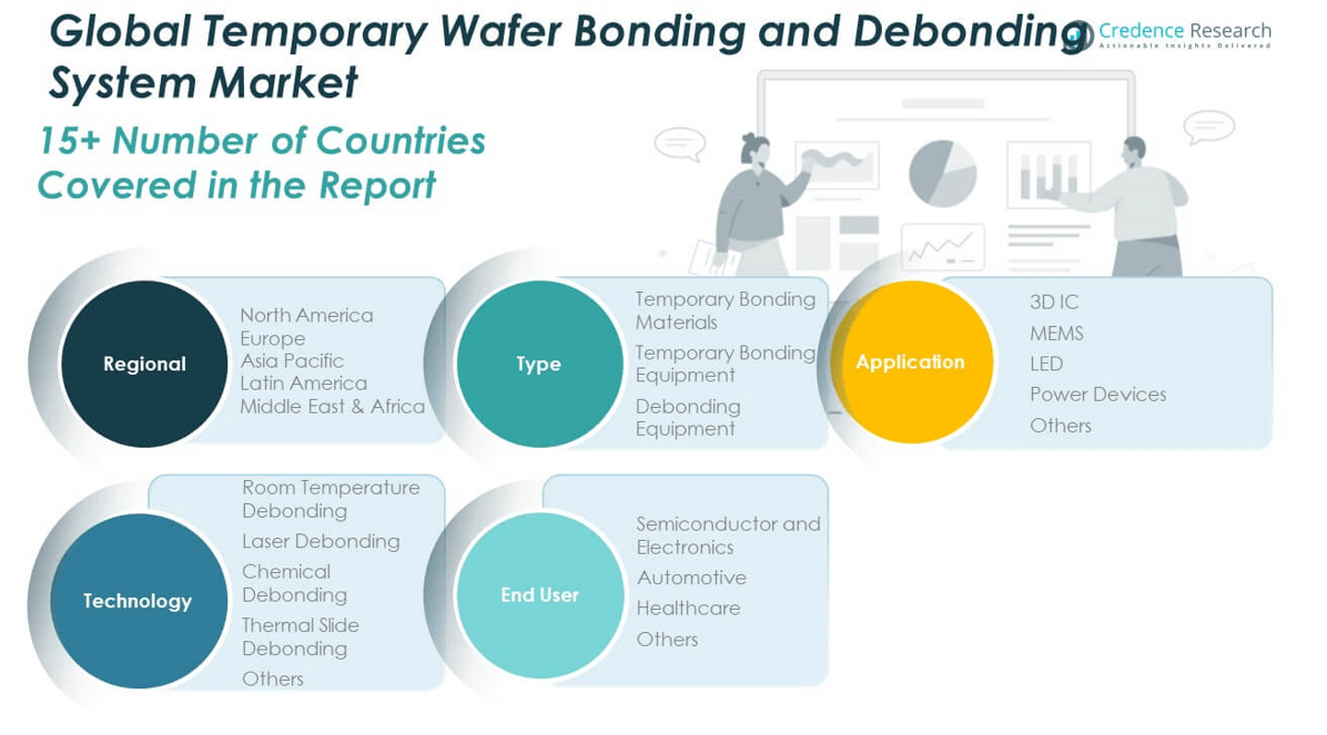
Segmentation:
By Type:
- Temporary Bonding Materials
- Temporary Bonding Equipment
- Debonding Equipment
By Application:
- 3D IC
- MEMS (Micro-Electro-Mechanical Systems)
- LED
- Power Devices
- Others
By Technology:
- Room Temperature Debonding
- Laser Debonding
- Chemical Debonding
- Thermal Slide Debonding
- Others
By End User:
- Semiconductor and Electronics
- Automotive
- Healthcare
- Others
By Region:
- North America
- Europe
- Germany
- France
- U.K.
- Italy
- Spain
- Rest of Europe
- Asia Pacific
- China
- Japan
- India
- South Korea
- South-east Asia
- Rest of Asia Pacific
- Latin America
- Brazil
- Argentina
- Rest of Latin America
- Middle East & Africa
- GCC Countries
- South Africa
- Rest of the Middle East and Africa
Regional Analysis:
The North America Temporary Wafer Bonding and Debonding System Market size was valued at USD 56.07 million in 2018 to USD 81.48 million in 2024 and is anticipated to reach USD 137.46 million by 2032, at a CAGR of 6.8% during the forecast period. North America holds a 21% share of the Global Temporary Wafer Bonding and Debonding System Market, supported by strong investments in semiconductor R&D, advanced packaging facilities, and government-led initiatives such as the CHIPS and Science Act. The region benefits from the presence of leading equipment manufacturers and foundries focusing on high-performance computing and AI-related chipsets. It continues to attract capital from both domestic and international players for fab expansions. Demand for wafer-level integration and robust backend processes has strengthened the adoption of bonding and debonding tools. The U.S. leads the regional market, followed by Canada, due to favorable innovation ecosystems. The region’s focus on onshoring semiconductor production is expected to sustain growth through the forecast period.
The Europe Temporary Wafer Bonding and Debonding System Market size was valued at USD 34.91 million in 2018 to USD 48.67 million in 2024 and is anticipated to reach USD 74.29 million by 2032, at a CAGR of 5.4% during the forecast period. Europe accounts for 13% of the Global Temporary Wafer Bonding and Debonding System Market, with strong activity in Germany, the Netherlands, and France. The region emphasizes industrial electronics, automotive chips, and sensor technologies, which rely on advanced packaging techniques. It supports sustainable chipmaking practices and is driving innovation in photonics and MEMS devices. Equipment demand is fueled by both integrated device manufacturers and third-party packaging specialists. The EU’s semiconductor strategy and national-level incentives are improving infrastructure and funding for high-tech processing tools. It remains a critical region for suppliers offering environmentally compliant and precision-based equipment solutions.
The Asia Pacific Temporary Wafer Bonding and Debonding System Market size was valued at USD 79.44 million in 2018 to USD 121.71 million in 2024 and is anticipated to reach USD 217.40 million by 2032, at a CAGR of 7.5% during the forecast period. Asia Pacific dominates the Global Temporary Wafer Bonding and Debonding System Market with a market share of 40%, driven by its position as the world’s largest semiconductor manufacturing hub. Countries like China, Taiwan, South Korea, and Japan house major foundries, OSAT providers, and packaging technology developers. The market is growing rapidly due to domestic chip demand, expanding consumer electronics production, and proactive government policies. It attracts substantial foreign direct investment into wafer processing infrastructure and backend facilities. Equipment suppliers gain opportunities through the establishment of new fabs and technology collaborations. The region’s advanced and cost-sensitive market drives innovation and pricing efficiency.
The Latin America Temporary Wafer Bonding and Debonding System Market size was valued at USD 9.26 million in 2018 to USD 13.51 million in 2024 and is anticipated to reach USD 20.19 million by 2032, at a CAGR of 5.1% during the forecast period. Latin America represents 5% of the Global Temporary Wafer Bonding and Debonding System Market, with steady demand emerging from Brazil and Mexico. The region is gradually building semiconductor capabilities to serve automotive, aerospace, and consumer electronics industries. It is benefiting from regional partnerships, university-led research programs, and government-led tech development funds. Local assembly units are starting to adopt temporary bonding systems for sensor packaging and MEMS fabrication. Market growth is influenced by economic stability, skilled labor development, and access to global supply chains. Equipment vendors exploring this region focus on cost-effective, scalable systems for small to mid-volume production.
The Middle East Temporary Wafer Bonding and Debonding System Market size was valued at USD 5.30 million in 2018 to USD 7.16 million in 2024 and is anticipated to reach USD 10.15 million by 2032, at a CAGR of 4.4% during the forecast period. The Middle East holds a 3% share in the Global Temporary Wafer Bonding and Debonding System Market. The region is focusing on diversifying its economy with investments in smart technologies, including sensors, IoT, and defense electronics, which indirectly boost semiconductor-related infrastructure. It is witnessing interest from global equipment suppliers looking to establish footprints through partnerships and technology exchanges. Countries such as the UAE and Saudi Arabia are exploring opportunities in localized chip assembly and R&D. It presents a long-term potential for expansion, particularly with innovation hubs and tech cities under development. Market traction depends on continued funding and collaboration with established global players.
The Africa Temporary Wafer Bonding and Debonding System Market size was valued at USD 3.59 million in 2018 to USD 5.75 million in 2024 and is anticipated to reach USD 8.04 million by 2032, at a CAGR of 4.2% during the forecast period. Africa contributes less than 2% to the Global Temporary Wafer Bonding and Debonding System Market but shows early signs of interest in semiconductor development. Countries like South Africa and Nigeria are exploring digital infrastructure and electronics manufacturing for economic growth. It presents an opportunity for long-term market development through capacity-building, academic research, and collaboration with international semiconductor firms. Growth is currently constrained by infrastructure and capital investment limitations. Governments and regional organizations are initiating technology-driven programs to develop skilled labor and innovation hubs. It remains an emerging market with slow but steady adoption potential.
Shape Your Report to Specific Countries or Regions & Enjoy 30% Off!
Key Player Analysis:
- EV Group (EVG)
- SÜSS MicroTec SE
- Tokyo Electron Limited (TEL)
- Disco Corporation
- Dynatex International
- AYUMI Industry Co., Ltd.
- 3M Company
Competitive Analysis:
The Global Temporary Wafer Bonding and Debonding System Market is characterized by strong competition among established semiconductor equipment manufacturers and specialized bonding technology providers. Key players such as EV Group, SUSS MicroTec, Tokyo Electron Limited, and Brewer Science dominate the market through advanced R&D capabilities, strategic partnerships, and global service networks. These companies focus on expanding their portfolios with systems that support a wide range of bonding materials and wafer types, while also enhancing throughput and precision. It remains highly innovation-driven, with competitors investing in process automation, cleanroom-compatible designs, and AI-based monitoring to improve yield and process control. New entrants face challenges due to high technical barriers and the capital-intensive nature of the equipment. Strategic collaborations with semiconductor foundries and research institutes are essential for technology validation and commercial adoption. Market participants differentiate through scalability, process flexibility, and support for emerging applications in heterogeneous integration and compound semiconductors.
Recent Developments:
- In Feb 2025, EV Group launched its latest temporary wafer bonding system. This new product is designed with enhanced precision and increased throughput capabilities, aiming to advance semiconductor manufacturing processes and address the growing demand for high-performance wafer-level packaging.
- In December 2024, Tokyo Electron launched its Ulucus™ LX Extreme Laser Lift Off (XLO) system for 300 mm wafers, reflecting technology development rather than any acquisition
Market Concentration & Characteristics:
The Global Temporary Wafer Bonding and Debonding System Market is moderately concentrated, with a few key players controlling a significant share of global revenue. It features a high degree of technological specialization, driven by precision engineering requirements and material compatibility across diverse semiconductor applications. Companies compete based on innovation, customization capabilities, and process integration with existing semiconductor manufacturing lines. The market demands consistent product performance, clean debonding, and support for ultrathin wafer processing. It exhibits high entry barriers due to the capital-intensive nature of equipment development, long qualification cycles, and the need for strong customer relationships. Vendors typically engage in long-term partnerships with foundries and research institutions to co-develop application-specific solutions.
Report Coverage:
The research report offers an in-depth analysis based on by type, application, technology, and end user. It details leading market players, providing an overview of their business, product offerings, investments, revenue streams, and key applications. Additionally, the report includes insights into the competitive environment, SWOT analysis, current market trends, as well as the primary drivers and constraints. Furthermore, it discusses various factors that have driven market expansion in recent years. The report also explores market dynamics, regulatory scenarios, and technological advancements that are shaping the industry. It assesses the impact of external factors and global economic changes on market growth. Lastly, it provides strategic recommendations for new entrants and established companies to navigate the complexities of the market.
Future Outlook:
- Increasing adoption of heterogeneous integration will drive demand for versatile bonding and debonding systems.
- Expansion of 3D IC and system-in-package technologies will support sustained market growth.
- Rising investment in AI, IoT, and automotive electronics will fuel advanced wafer-level packaging requirements.
- Integration of smart monitoring and AI-driven process control will enhance system efficiency and yield.
- Growth of compound semiconductor applications will create new opportunities for non-silicon wafer handling.
- Miniaturization in healthcare and wearable devices will open niche application areas.
- Equipment manufacturers will expand presence in emerging markets through localized support and partnerships.
- Demand for flexible, modular tools will rise with increased fab diversification and customization.
- Strong government funding and semiconductor policy initiatives will strengthen global manufacturing capacity.
- Continued focus on clean debonding and surface preservation will drive R&D and product innovation.