Market Overview
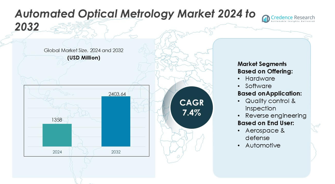
Automated Optical Metrology Market size was valued USD 1358 million in 2024 and is anticipated to reach USD 2403.64 million by 2032, at a CAGR of 7.4% during the forecast period.
| REPORT ATTRIBUTE |
DETAILS |
| Historical Period |
2020-2023 |
| Base Year |
2024 |
| Forecast Period |
2025-2032 |
| Automated Optical Metrology Market Size 2024 |
USD 1358 million |
| Automated Optical Metrology Market, CAGR |
7.4% |
| Automated Optical Metrology Market Size 2032 |
USD 2403.64 million |
The Automated Optical Metrology Market features a concentrated group of global technology vendors that enhance manufacturing precision in Australia’s industrial ecosystem, particularly within sectors such as semiconductors, automotive components, and advanced materials. These companies strengthen their presence by offering high-resolution 3D measurement systems, inline inspection platforms, and AI-enhanced defect-detection tools that support the country’s shift toward highly automated production lines. Asia Pacific stands as the leading region in the broader market, holding an exact 30% market share, driven by extensive semiconductor fabrication activity, strong electronics manufacturing capacity, and rapid adoption of digital-quality assurance technologies across emerging industrial clusters.
Market Insights
- The market was valued at USD 1358 million in 2024 and is projected to reach USD 2403.64 million by 2032 at a 7.4% CAGR, reflecting steady global adoption.
- Demand rises as industries prioritize precision manufacturing, with semiconductor fabrication and automotive components driving accelerated uptake of high-resolution 3D and inline optical inspection systems.
- AI-enabled defect detection, real-time quality control, and advanced 3D metrology capabilities emerge as key trends shaping technological differentiation among vendors.
- Competitive intensity increases as technology providers expand automation-ready platforms, while high system costs and integration complexity remain notable restraints for smaller manufacturers.
- Asia Pacific leads the market with a 30% share, supported by strong electronics production, while hardware remains the dominant offering segment with a 62% share, reinforcing its role in high-accuracy measurement workflows.
Access crucial information at unmatched prices!
Request your sample report today & start making informed decisions powered by Credence Research Inc.!
Download Sample
Market Segmentation Analysis:
By Offering
Hardware dominates the Automated Optical Metrology Market with an exact 62% market share, driven by the widespread adoption of high-resolution 3D sensors, laser scanners, and structured-light systems that support precise dimensional analysis. Manufacturers prioritize hardware investments to enhance throughput, reduce measurement errors, and support in-line automation across production lines. Demand rises further as industries shift toward real-time defect detection and non-contact measurement capabilities. Software and services expand steadily as analytics, data-driven optimization, and system integration requirements grow, but hardware remains the primary revenue contributor due to its critical role in measurement accuracy.
- For instance, Nikon Metrology Inc’s iNEXIV VMA-2520 video measuring system offers a minimum readout resolution of 0.1 µm and can handle samples with guaranteed accuracy up to 15 kg, enabling high-precision dimensional inspection over a 250 × 200 × 200 mm measurement range with multi-sensor vision and optional touch probe adaptability.
By Application
Quality Control & Inspection emerges as the leading application segment, holding an exact 57% market share, supported by its essential role in ensuring compliance, detecting micro-level defects, and improving production reliability. Automated optical systems enable faster inspection cycles, higher repeatability, and reduced human dependency across mass-manufacturing environments. Reverse engineering and mapping & modelling gain traction as digital-twin adoption increases, but remain secondary in overall deployment volume. The dominance of quality control aligns with stringent industry regulations and the rising need for inline, high-precision verification in semiconductor, automotive, and aerospace operations.
- For instance, Carl Zeiss AG advances this segment through systems such as the ZEISS O-INSPECT 543, which delivers a multisensor measuring accuracy of Eₘₐₓ = 1.9 µm + L/250 µm and supports tactile probing forces below 0.1 N, and the ZEISS METROTOM 6 Scout CT scanner capable of 3 µm voxel resolution, enabling nondestructive inspection of complex assemblies with traceable metrology precision.
By End-User
The Semiconductor sector leads the market with an exact 41% market share, driven by its reliance on nanometer-scale inspection, wafer measurement, and photolithography alignment workflows that require ultra-high-precision metrology. The industry’s continuous node shrinkage and defect-density reduction targets strengthen demand for automated, high-resolution optical systems. Automotive and aerospace & defense follow as key adopters for dimensional validation and component integrity assessments, while general manufacturing expands usage with the rise of smart factories. However, semiconductors remain the highest-value end-user due to stringent accuracy requirements and rapid innovation cycles.
Key Growth Drivers
Rising Demand for Precision Manufacturing
The market experiences strong growth as industries adopt precision manufacturing practices that require micron-level accuracy in inspection and measurement. Automated optical metrology enables high repeatability, non-contact evaluation, and real-time defect identification, supporting tighter engineering tolerances across semiconductor, aerospace, and automotive applications. The shift toward advanced production platforms, including EUV lithography, EV component miniaturization, and lightweight aerospace structures, reinforces system adoption. Enhanced measurement consistency and reduced manual intervention further position automated optical metrology as a core enabler of modern high-performance manufacturing ecosystems.
- For instance, Optical Metrology Services Ltd (OMS) reinforces the industry shift toward digital quality assurance through the use of high-accuracy 3D scanning systems and calibrated photogrammetry rigs.
Expansion of Inline and Real-Time Quality Control
Growth accelerates as manufacturers transition from offline inspection to inline, automated quality assurance frameworks to reduce scrap rates and accelerate throughput. Automated optical metrology systems integrate seamlessly with production lines, providing continuous monitoring and rapid feedback during critical fabrication steps. Their ability to detect micro-defects, validate component geometry, and provide instant process corrections enhances productivity in high-volume industries. This real-time capability supports lean manufacturing initiatives, improves operational efficiency, and enables proactive process control, making automated inspection essential for competitive, cost-optimized industrial operations.
- For instance, Hexagon AB advances industrial manufacturing transformation through systems like the Leica Absolute Tracker AT960, which offers high-speed dynamic measurement for real-time machine control, and through its WLS400A white-light scanning cells.
Increasing Adoption in Semiconductor Fabrication
Semiconductor fabs drive substantial market momentum as device geometries shrink and defect tolerances tighten. Automated optical metrology tools offer nanometer-scale resolution for wafer topography analysis, overlay measurement, and pattern fidelity verification. Their use expands with advanced nodes, 3D NAND structures, and heterogeneous chip packaging requiring complex multi-layer inspection. The industry’s push for yield optimization, cycle-time reduction, and improved process uniformity strengthens demand. As lithography transitions to more intricate architectures, automated optical metrology becomes indispensable for ensuring device reliability and fab-level manufacturing precision.
Key Trends & Opportunities
Growth of AI-Integrated Metrology Solutions
AI and machine learning enable faster defect classification, pattern recognition, and process prediction, creating major opportunities for intelligent metrology platforms. Automated optical systems increasingly embed AI algorithms to reduce false detections, enhance measurement accuracy, and provide predictive analytics for proactive maintenance. This trend supports faster decision-making in semiconductor, automotive, and electronics manufacturing. The integration of AI-powered analytics also enables automated root-cause identification and adaptive process tuning, opening pathways for next-generation smart inspection systems aligned with Industry 4.0 strategies.
- For instance, Encirc reduced the weight of Belu Mineral Water’s bottles by 20g, which helped save 850,000 kg of glass annually for that specific client. This was achieved through new techniques and the production of lighter containers.
Expansion of 3D Optical Metrology and Digital Twin Adoption
3D metrology technologies gain traction as industries accelerate digital-twin deployment, requiring accurate geometric mapping and high-resolution structural analysis. Automated optical systems support rapid 3D modelling for virtual simulation, part validation, and process optimization. Opportunities emerge as aerospace, automotive, and precision engineering companies adopt structured-light scanners and laser-based 3D measurement tools for complex surface inspection. The growing emphasis on virtual prototyping and simulation-driven design enhances demand for optical metrology solutions that enable rich data capture and seamless integration with digital manufacturing frameworks.
- For instance, Ardagh commissioned its NextGen hybrid furnace in Obernkirchen, achieving a 64 % reduction in emissions per bottle at that line.It built a hydrogen electrolyser in Limmared (Sweden) to feed low-carbon hydrogen into its glass melting system.
Surge in Demand from EV and Advanced Materials Manufacturing
The shift toward electric vehicles and advanced material systems creates new opportunities for automated optical metrology. EV batteries, lightweight composites, and high-precision drivetrain components require stringent dimensional validation and defect detection. Optical metrology tools support high-throughput inspection for electrode coatings, cell assembly, and composite structural integrity. As OEMs invest in next-generation gigafactories and high-precision production lines, the adoption of automated optical inspection accelerates. This trend strengthens the market’s position within rapidly evolving clean-mobility and advanced-materials supply chains.
Key Challenges
High Initial Investment and Integration Complexity
Automated optical metrology systems involve high capital expenditure, particularly for advanced 3D scanners, interferometers, and semiconductor-grade inspection tools. Integrating these systems into existing production lines requires specialized engineering expertise, calibration cycles, and software alignment. Small and mid-size manufacturers often face budget constraints that limit adoption. Additionally, the need for customized setups and compatibility with diverse manufacturing environments increases implementation complexity. These factors slow deployment across cost-sensitive industries and create barriers for companies transitioning from manual or semi-automated inspection processes.
Technical Limitations with Complex Surfaces and Reflective Materials
Despite technological progress, automated optical metrology faces challenges when measuring highly reflective, transparent, or irregular surfaces. Variations in light scattering, surface absorption, and material reflectance can reduce measurement accuracy and require additional pre-processing or specialized optics. Industries working with glass, polished metals, or multi-layer semiconductor structures often encounter issues related to signal distortion and insufficient feature contrast. These limitations increase the need for hybrid inspection solutions, material-specific calibration, and advanced illumination techniques, which may increase system cost and operational complexity.
Regional Analysis
North America
North America holds a 34% market share, supported by strong adoption of high-precision inspection technologies across semiconductor, aerospace, and advanced manufacturing sectors. The region benefits from substantial investments in nanofabrication, EV component production, and defense-grade metrology systems that demand micron and sub-micron accuracy. Leading technology suppliers and research institutions contribute to rapid innovation in 3D optical scanning, inline inspection, and AI-driven defect analytics. Government emphasis on manufacturing modernization further accelerates deployment, making North America a core hub for advanced optical metrology development and commercialization.
Europe
Europe accounts for an exact 28% market share, driven by strong industrial automation, stringent manufacturing quality standards, and expanding use of optical inspection in automotive, aerospace, and precision engineering industries. German and Nordic manufacturers lead adoption due to robust investments in Industry 4.0 and digital-quality ecosystems. The region’s focus on sustainability and lightweight material engineering increases reliance on high-resolution metrology for component validation. Semiconductor ecosystem growth in Germany and the Netherlands further enhances demand. Europe maintains steady momentum as companies prioritize accuracy, regulatory compliance, and production efficiency.
Asia Pacific
Asia Pacific secures a 30% market share, emerging as one of the fastest-growing regional markets due to strong semiconductor fabrication activity in China, Taiwan, South Korea, and Japan. Expanding electronics manufacturing, EV battery production, and large-scale industrial automation initiatives drive widespread adoption of high-speed optical inspection tools. The region benefits from investment in advanced wafer-inspection facilities, precision machining, and metrology-enabled quality control for mass production. Rising deployment of 3D sensors, structured-light systems, and real-time inspection platforms strengthens Asia Pacific’s position as a global center for high-volume, precision-driven manufacturing.
Latin America
Latin America holds a 5% market share, with adoption gradually increasing as manufacturing modernization accelerates in automotive, electronics assembly, and metal fabrication industries. Countries such as Mexico and Brazil invest in automated inspection tools to enhance product consistency and reduce rework rates. Growth is further supported by the expansion of export-oriented production clusters demanding higher quality assurance standards. Although technological penetration remains lower compared with major regions, infrastructure upgrades, increased foreign investment, and the rise of regional electronics suppliers continue to strengthen the long-term outlook for automated optical metrology solutions.
Middle East & Africa
The Middle East & Africa region accounts for 3% market share, driven primarily by growing automation initiatives within energy, aerospace maintenance, and industrial manufacturing sectors. Gulf countries invest in metrology technologies to support diversification into advanced industries and improve quality control in high-value engineering projects. Adoption remains in an early phase but is rising with increased localization of manufacturing capabilities and partnerships with global technology suppliers. Infrastructure expansion, industrial digitization programs, and investments in precision engineering education contribute to progressive but steady uptake of automated optical inspection systems.
Market Segmentations:
By Offering:
By Application:
- Quality control & inspection
- Reverse engineering
By End User:
- Aerospace & defense
- Automotive
By Geography
- North America
- Europe
- Germany
- France
- U.K.
- Italy
- Spain
- Rest of Europe
- Asia Pacific
- China
- Japan
- India
- South Korea
- South-east Asia
- Rest of Asia Pacific
- Latin America
- Brazil
- Argentina
- Rest of Latin America
- Middle East & Africa
- GCC Countries
- South Africa
- Rest of the Middle East and Africa
Competitive Landscape
The competitive landscape in the Automated Optical Metrology Market players such as Verus Precision Ltd, Intertek Group plc, Nikon Metrology Inc., Dimensional Metrology Services, Carl Zeiss AG, Optical Metrology Services Ltd, Metalock Engineering Group, Renishaw plc, Hexagon AB, and Quality Vision International Inc. the Automated Optical Metrology Market reflects rapid technological advancement, expanding industrial automation, and increasing demand for ultra-precise inspection systems across high-value manufacturing environments. Companies strengthen their market position by developing high-speed 3D measurement platforms, AI-driven defect detection tools, and automation-ready inline inspection solutions that support real-time quality assurance. The shift toward semiconductor miniaturization, EV component validation, and aerospace-grade dimensional accuracy accelerates investment in advanced optical sensors and scalable metrology architectures. Vendors also expand service portfolios through system integration, calibration, and cloud-based analytics, creating differentiated value for customers. Continuous innovation, strong R&D pipelines, and strategic partnerships with OEMs reinforce competitiveness and drive sustained market growth.
Shape Your Report to Specific Countries or Regions & Enjoy 30% Off!
Key Player Analysis
- Verus Precision Ltd
- Intertek Group plc
- Nikon Metrology Inc.
- Dimensional Metrology Services
- Carl Zeiss AG
- Optical Metrology Services Ltd
- Metalock Engineering Group
- Renishaw plc
- Hexagon AB
- Quality Vision International Inc.
Recent Developments
- In May 2025, ZEISS launched the Smartzoom 100 an advanced digital microscope for industry, praised for its high-resolution images, user-friendly interface for non-experts, and ergonomic design (no eyepieces) for better quality assurance, failure analysis, and collaboration in manufacturing. It simplifies complex optical tasks, making microscopy accessible for faster, fatigue-free inspections across various industrial sectors.
- In March 2024, Hitachi High-Tech’s of the LS9300AD wafer inspection system brings advanced detection for subtle defects like shallow scratches and contamination on unpatterned wafers, using new DIC (Differential Interference Contrast) optics alongside traditional laser scattering, to boost speed, efficiency, and yields for complex semiconductor manufacturing.
- In October 2023, Hexagon’s Manufacturing Intelligence division has introduced the HP-L-10.10 LITE laser scanner for coordinate measuring machines (CMMs), offering a cost-effective solution for efficient surface measurement and higher throughput.
Report Coverage
The research report offers an in-depth analysis based on Offering, Application, End-User and Geography. It details leading market players, providing an overview of their business, product offerings, investments, revenue streams, and key applications. Additionally, the report includes insights into the competitive environment, SWOT analysis, current market trends, as well as the primary drivers and constraints. Furthermore, it discusses various factors that have driven market expansion in recent years. The report also explores market dynamics, regulatory scenarios, and technological advancements that are shaping the industry. It assesses the impact of external factors and global economic changes on market growth. Lastly, it provides strategic recommendations for new entrants and established companies to navigate the complexities of the market.
Future Outlook
- The market will accelerate with rising adoption of inline, real-time inspection across high-volume manufacturing lines.
- Semiconductor fabrication will drive substantial demand for nanometer-level optical metrology capabilities.
- AI and machine learning integration will enhance defect detection accuracy and reduce inspection cycle times.
- 3D optical metrology systems will gain wider use in digital-twin workflows and simulation-driven engineering.
- EV battery, electronics, and advanced materials manufacturing will emerge as major growth verticals.
- Automation-ready optical systems will expand as factories transition toward fully digital quality ecosystems.
- Cloud-enabled analytics will support remote monitoring, predictive maintenance, and multi-site quality standardization.
- Miniaturization trends in components will increase the need for high-resolution, non-contact inspection tools.
- Compact, portable optical scanners will see rising adoption in field inspection and maintenance applications.
- Collaboration between metrology vendors and OEMs will strengthen to deliver customized, sector-specific inspection solutions.


