Home » Semiconductor & Electronics » Semiconductor Bonder Machine Market

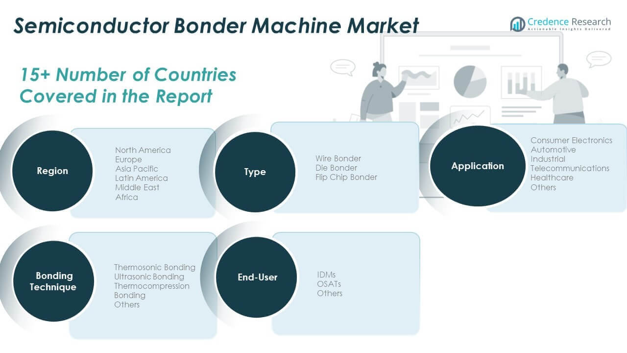
Semiconductor Bonder Machine Market By Type (Wire Bonder, Die Bonder, Flip Chip Bonder); By Application (Consumer Electronics, Automotive, Industrial, Telecommunications, Healthcare, Others); By Bonding Technique (Thermosonic Bonding, Ultrasonic Bonding, Thermocompression Bonding, Others); By End-User (IDMs, OSATs, Others); By Region – Growth, Share, Opportunities & Competitive Analysis, 2024 – 2032

Report ID: 10581 | Report Format : Excel, PDF

Market Overview:

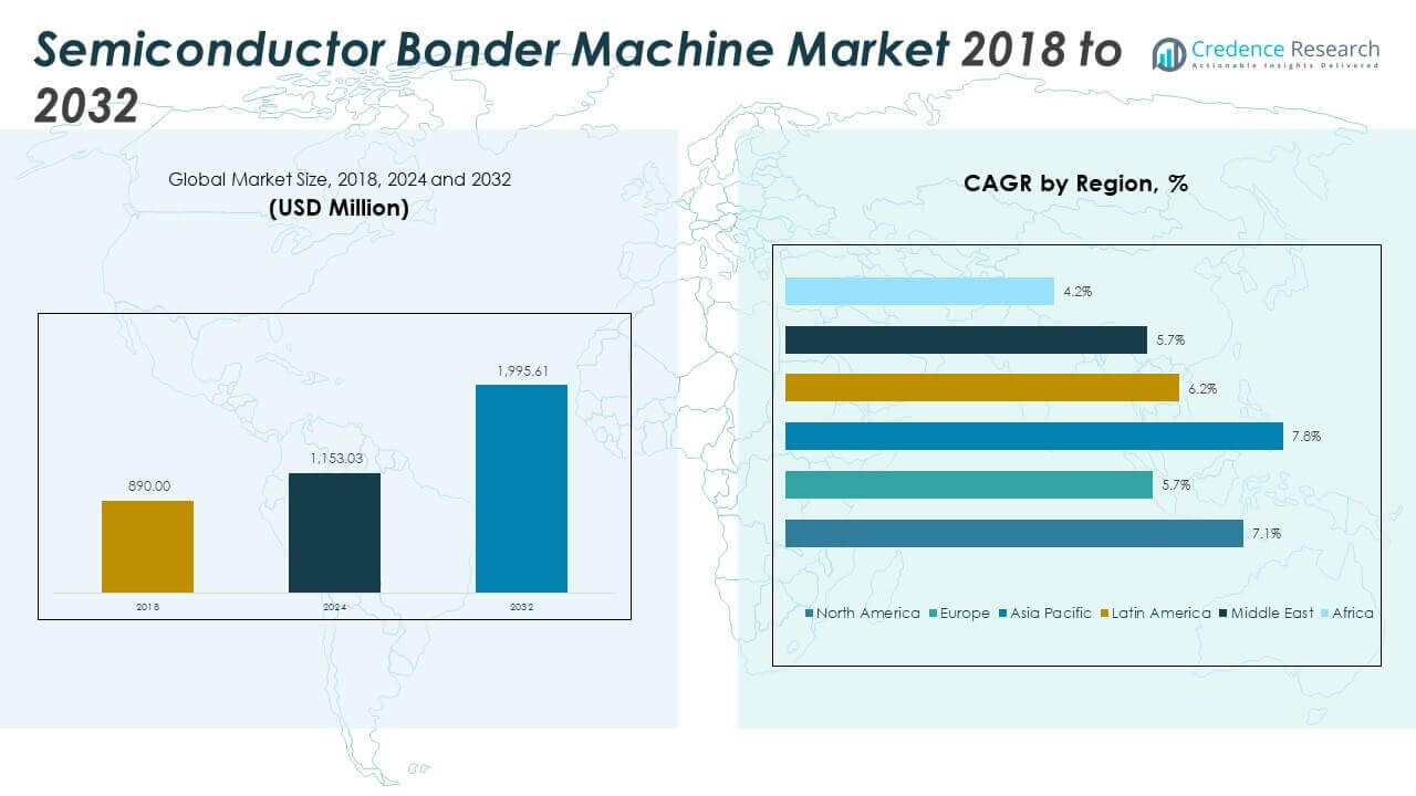
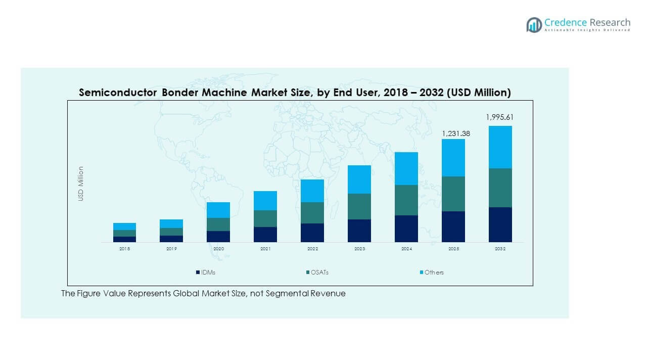
The Semiconductor Bonder Machine Market size was valued at USD 890.00 million in 2018 to USD 1,153.03 million in 2024 and is anticipated to reach USD 1,995.61 million by 2032, at a CAGR of 7.14% during the forecast period.

REPORT ATTRIBUTE DETAILS
Historical Period 2020-2023
Base Year 2024
Forecast Period 2024-2032
Semiconductor Bonder Machine Market Size 2024 USD 1,153.03 million
Semiconductor Bonder Machine Market, CAGR 7.14%
Semiconductor Bonder Machine Market Size 2032 USD 1,995.61 million


Market growth is driven by rising demand for heterogeneous integration, miniaturized consumer electronics, and electric vehicle power modules. As chip complexity increases, manufacturers require precision bonding for advanced 2.5D and 3D packaging formats. Wide bandgap materials such as GaN and SiC in automotive and energy sectors further fuel equipment upgrades. The integration of AI in bonding platforms enhances process control, improves throughput, and reduces defect rates. These factors push OSATs and IDMs to adopt high-speed, sub-micron accurate bonders tailored to new-generation logic and memory devices.

Asia Pacific dominates due to its dense semiconductor manufacturing base across China, Taiwan, South Korea, and Japan. These regions lead in OSAT capacity and backend investment, supported by public incentives and fab expansion. North America and Europe follow with demand from high-end R&D and automotive electronics. The U.S. benefits from reshoring and strategic chip investments. Emerging regions like Southeast Asia and India show strong potential due to rising local production, favorable trade policies, and increasing demand for localized packaging capabilities.

Semiconductor Bonder Machine Market Size

Market Insights:

  • The Semiconductor Bonder Machine Market was valued at USD 890.00 million in 2018, reached USD 1,153.03 million in 2024, and is projected to attain USD 1,995.61 million by 2032, expanding at a CAGR of 7.14%, supported by advanced packaging adoption and backend capacity expansion.
  • Asia Pacific, North America, and Europe lead with 53.4%, 20.9%, and 14.2% market share respectively, driven by strong OSAT concentration, large IDM presence, and sustained investment in automotive and industrial electronics.
  • Asia Pacific is the fastest-growing region and already holds 53.4% share, supported by aggressive fab expansion in China, Taiwan, South Korea, and rising backend localization across Southeast Asia.
  • By regional distribution, Asia Pacific dominates with over half of global demand, reflecting its role as the primary hub for semiconductor assembly, packaging, and export-oriented manufacturing.
  • North America and Europe together account for over 35% of market share, supported by advanced R&D activity, automotive semiconductor demand, and reshoring-focused manufacturing initiatives.

Access crucial information at unmatched prices!

Request your sample report today & start making informed decisions powered by Credence Research Inc.!

Download Sample

Market Drivers

Surging Demand for Heterogeneous Integration and Advanced 3D Packaging Architectures

The need for compact, high-performance semiconductor devices fuels growth in 3D packaging. Heterogeneous integration allows multiple chiplets to function as a single unit, improving speed and efficiency. This drives the adoption of hybrid bonding and precision bonder machines. The Semiconductor Bonder Machine Market grows as fabs and OSATs shift to advanced interconnects. These technologies demand tight bond line control and sub-micron accuracy. Bonders with high throughput and real-time process monitoring gain preference. Players invest in adaptive alignment systems to handle smaller nodes. Packaging for AI, data center, and consumer chips directly supports this growth. Demand from logic and memory packaging accelerates high-end equipment purchases.

Strong Expansion of Automotive Electronics and Power Semiconductor Packaging Requirements

Electric vehicles and ADAS modules require high-reliability packaging methods. Wire and die bonders must handle wide bandgap materials like GaN and SiC. These materials need strong thermal control and robust bond interfaces. The Semiconductor Bonder Machine Market benefits from growing EV production and electrification trends. Equipment vendors adapt machines for high-voltage and high-frequency semiconductor packaging. Automotive supply chains invest in automation to meet scale and quality goals. High-yield bonding supports safety-critical chip performance. Power module packaging sees increasing demand for vacuum die bonders. SiC adoption across EV inverters creates new opportunities for bonder equipment suppliers.

  • For instance, Palomar Technologies’ 3880‑II die bonder offers support for GaN/GaAs MMIC and power electronics applications with flexible die‑bonding options including thermocompression and epoxy die attach.

High Investment Momentum in Semiconductor Fabs and OSAT Infrastructure Across Asia-Pacific

Asia-Pacific accounts for the largest share of semiconductor assembly and packaging operations. Countries such as China, Taiwan, and South Korea lead in backend process investment. OSAT players and integrated device manufacturers expand capacity to serve global chip demand. The Semiconductor Bonder Machine Market gains from this regional momentum. Governments in these countries offer incentives for advanced manufacturing. Local bonder machine makers grow through partnerships with leading chip houses. Equipment demand rises in tandem with fab expansions. Players seek machines with low cost of ownership and high equipment uptime. Localization efforts further increase bonder machine procurement across the region.

Increasing Focus on Precision, Flexibility, and Miniaturization in Consumer Electronics Devices

The rapid evolution of smartphones, wearables, and AR/VR devices pushes packaging density. Manufacturers require bonders capable of ultra-fine pitch, low-k material handling, and chip stacking. High-precision bonders support innovations in thinner, faster mobile components. The Semiconductor Bonder Machine Market benefits from this miniaturization wave. Bonding accuracy and adaptive force control are key performance metrics. Machines need to accommodate different package types with minimal changeover time. Flexibility in software, tooling, and process flow becomes essential. Consumer OEMs push for smaller footprints and higher yield. Equipment vendors respond with compact, multi-purpose bonding systems for diverse applications.

  • For example, Finetech’s FINEPLACER® femto 2 automatic bonder is documented to deliver placement accuracy around 0.3 µm (300 nm) in manufacturer specifications. This high‑precision capability makes it suitable for fine‑pitch MEMS, optical assemblies, and advanced sensor applications. The ~0.3 µm accuracy figure is referenced in Finetech’s official technical literature.

Market Trends

Adoption of AI-Enabled Bonding Systems to Improve Accuracy, Yield, and Self-Calibration

Machine learning tools now enhance bonder intelligence and precision in process control. AI-driven platforms enable defect prediction, dynamic path correction, and real-time optimization. These systems reduce bonding errors and increase productivity through predictive analytics. The Semiconductor Bonder Machine Market adopts these smart systems to lower cost per package. AI tools also support automated decision-making and predictive maintenance. Equipment with AI modules improves learning across multiple production batches. Smart bonding tools align well with Industry 4.0 factory integration. Real-time quality inspection via vision systems enhances process feedback. AI-enabled machines raise uptime and deliver faster time-to-yield.

Transition to Full Automation with Flexible and Modular Bonder Configurations for High-Mix Fabs

Flexible fab operations demand configurable bonding platforms with modular architectures. These machines handle diverse substrates, package types, and throughput needs. Operators seek seamless integration with material handling and post-bond inspection units. The Semiconductor Bonder Machine Market aligns with this shift to smart, automated lines. Fully automated modules reduce operator dependency and improve safety. Modular bonders support faster product changeovers, improving fab agility. Equipment designs now focus on space efficiency and ergonomic access. Fabless firms and OSATs adopt configurable systems to manage product variety. Remote monitoring and process logging features become essential in modern bonding setups.

  • For instance, ASMPT’s Eagle AERO wire bonder delivers up to 30% higher units per hour (UPH) in copper wire applications, supporting greater throughput in high-volume production environments.

Rapid Adoption of Hybrid Bonding for Next-Generation Logic and Memory Stacking Applications

Hybrid bonding combines wafer-to-wafer and die-to-wafer techniques for high-density interconnects. It enables direct copper-to-copper contact, eliminating need for solder bumps. This method supports 3D NAND, DRAM stacking, and AI accelerators. The Semiconductor Bonder Machine Market sees growing use of hybrid bonders in logic-memory co-packaging. Equipment must maintain sub-1µm alignment and handle ultra-clean bonding environments. Bonding tools now include plasma activation and thermal compression in one platform. Demand grows from foundries investing in advanced packaging lines. Hybrid bonding supports higher bandwidth and lower power in HPC chips. Advanced node technologies depend on this precision bonding method.

  • For instance, BE Semiconductor Industries (Besi) secured orders for its latest hybrid bonding systems that incorporate ~100 nm placement accuracy, supporting high‑density interconnects for advanced packaging.

Increased Role of Collaborative Partnerships Between Equipment Vendors and Chip Manufacturers

Strategic partnerships drive innovation in bonder machine development and customization. Equipment makers co-develop solutions with chipmakers to meet unique process demands. Collaborative engineering enables faster qualification and time-to-market for new devices. The Semiconductor Bonder Machine Market benefits from deep integration into advanced packaging roadmaps. Joint test lines and pilot runs improve tool design and validation. These partnerships also secure long-term purchase commitments. Vendors gain insights into future chip design needs. Co-location of R&D hubs near foundries and OSATs becomes common. Closer cooperation shortens feedback loops and enhances bond performance optimization.

Semiconductor Bonder Machine Market Share

Market Challenges Analysis

High Equipment Costs and Limited ROI for Small and Mid-Sized Packaging Houses

Bonder machines with advanced features require high capital investment. Smaller OSATs and IDMs face cost barriers in adopting next-gen systems. Long payback cycles and limited customization reduce purchase willingness. The Semiconductor Bonder Machine Market must overcome these affordability hurdles. Maintenance and training costs add further strain on smaller operators. Entry-level models often lack features needed for high-complexity packaging. Financing options and service models vary across regions. Vendors must balance innovation with accessibility to penetrate broader segments. Price-performance trade-offs remain a key barrier to adoption for many small players.

Complex Process Integration and Equipment Qualification for Advanced Packaging Lines

Integrating bonders into heterogeneous packaging lines is technically complex. Variations in substrates, bonding materials, and device geometries challenge standardization. Each chip type may need unique bonding recipes and tool settings. The Semiconductor Bonder Machine Market deals with high calibration needs and operator training. Qualification timelines for new products are long and resource-intensive. Any drift in bond quality can affect downstream yields significantly. Matching thermal and mechanical stress profiles across layers adds complexity. Equipment compatibility with legacy and new processes limits flexibility. Process tuning remains time-consuming in multi-die, high-density packages.

Market Opportunities

Growing Interest in Advanced Packaging Among Foundries and Logic Chipmakers Globally

Foundries and fabless firms increasingly invest in backend innovation to boost performance. Packaging now plays a major role in chip scaling beyond Moore’s Law. The Semiconductor Bonder Machine Market benefits as firms adopt hybrid, 2.5D, and 3D structures. Equipment demand grows from logic chip suppliers focused on chiplet-based integration. New fab expansions in the U.S., India, and Southeast Asia open sales opportunities. Players seek scalable bonders with proven production track records. Machines with high accuracy and low contamination gain strong traction in these setups.

Emergence of Edge AI, Wearables, and Miniaturized IoT Devices Requiring High-Precision Bonding

Compact electronic devices demand ultra-small packages with strong interconnect performance. Consumer and industrial IoT growth drives tighter pitch and advanced stack requirements. The Semiconductor Bonder Machine Market sees new demand in this device category. Companies seek machines with adaptable bonding heads and real-time vision correction. Fast cycle time and low defect rates are essential to handle volume. Equipment makers with compact, multifunctional machines can gain share in this evolving segment.

Market Segmentation Analysis:

The Semiconductor Bonder Machine Market covers a wide range of equipment types, applications, techniques, and end-users.

By type, wire bonders lead due to extensive use in legacy and mid-range packaging formats. Die bonders follow, driven by demand in logic and power semiconductor packaging. Flip chip bonders show strong growth in high-end mobile, AI, and HPC chips due to finer interconnect and higher density needs.

  • For instance, Kulicke & Soffa’s Ultralux model achieves 25 wires per second with 2 mm wire length. Die bonders follow, driven by demand in logic and power semiconductor packaging.

By application, consumer electronics dominate due to smartphone, wearables, and tablet production. Automotive follows with rising use in EV power modules and ADAS systems. Industrial and telecom segments demand high-reliability bonding for sensors and base station ICs. Healthcare uses bonder machines in medical imaging and diagnostic device packaging.

  • For instance, Besi’s Datacon 8800 TC enables 2μm placement accuracy for telecom RF ICs. Healthcare uses bonder machines in medical imaging and diagnostic device packaging for instance, Finetech’s FINEPLACER femto 2 offers 250nm alignment for medical MEMS.

By bonding technique, thermosonic bonding holds the largest share, preferred for wire bonding in mass production. Ultrasonic bonding finds use in metal-to-metal joining for MEMS and RF devices. Thermocompression bonding supports fine-pitch logic and memory packages. Other techniques include adhesive and hybrid bonding used in advanced applications.

By end-user, OSATs lead in volume deployment due to contract packaging for global chipmakers. IDMs invest in high-end bonder machines for in-house advanced packaging. Others include research labs, niche packaging firms, and pilot lines supporting innovation.

Segmentation:

By Type

  • Wire Bonder
  • Die Bonder
  • Flip Chip Bonder

By Application

  • Consumer Electronics
  • Automotive
  • Industrial
  • Telecommunications
  • Healthcare
  • Others

By Bonding Technique

  • Thermosonic Bonding
  • Ultrasonic Bonding
  • Thermocompression Bonding
  • Others

By End-User

  • IDMs (Integrated Device Manufacturers)
  • OSATs (Outsourced Semiconductor Assembly and Test)
  • Others

By Region

  • North America
    • U.S.
    • Canada
    • Mexico
  • Europe
    • Germany
    • France
    • U.K.
    • Italy
    • Spain
    • Rest of Europe
  • Asia Pacific
    • China
    • Japan
    • India
    • South Korea
    • South-east Asia
    • Rest of Asia Pacific
  • Latin America
    • Brazil
    • Argentina
    • Rest of Latin America
  • Middle East & Africa
    • GCC Countries
    • South Africa
    • Rest of the Middle East and Africa

Regional Analysis:

North America

The North America Semiconductor Bonder Machine Market size was valued at USD 190.02 million in 2018 to USD 241.09 million in 2024 and is anticipated to reach USD 416.29 million by 2032, at a CAGR of 7.1% during the forecast period. North America accounts for approximately 15.9% of the global market share in 2024. It benefits from strong semiconductor R&D investments and a robust ecosystem of fabless chipmakers and IDMs. U.S.-based players lead in advanced packaging initiatives tied to AI, automotive, and data center applications. Government-backed efforts, including the CHIPS Act, strengthen local semiconductor manufacturing and backend assembly. Demand for hybrid bonding and flip-chip bonder systems is high in leading-edge packaging hubs. Equipment manufacturers serve advanced nodes and integrate AI-driven control systems into bonding platforms. Strategic partnerships between equipment vendors and top-tier foundries boost tool validation. Strong emphasis on automation and reliability sustains demand across automotive and industrial segments.

Europe

The Europe Semiconductor Bonder Machine Market size was valued at USD 135.28 million in 2018 to USD 163.47 million in 2024 and is anticipated to reach USD 254.94 million by 2032, at a CAGR of 5.8% during the forecast period. Europe holds about 10.8% share of the global market in 2024. Germany, France, and the Netherlands anchor regional growth through automotive electronics and MEMS packaging advancements. European players emphasize high-precision bonding for sensor modules, RF components, and photonics. The region sees increasing adoption of thermosonic and ultrasonic bonding in automotive and medical device applications. Equipment vendors align offerings with stringent EU quality and environmental standards. Collaborative research under EU semiconductor initiatives supports technology innovation. Bonding solutions with modularity and automation gain traction in high-mix, low-volume production setups. Public-private programs fuel ecosystem expansion for packaging innovation.

Asia Pacific

The Asia Pacific Semiconductor Bonder Machine Market size was valued at USD 465.47 million in 2018 to USD 615.54 million in 2024 and is anticipated to reach USD 1,118.14 million by 2032, at a CAGR of 7.8% during the forecast period. Asia Pacific dominates the global Semiconductor Bonder Machine Market with a 40.5% share in 2024. The region leads due to dense OSAT networks, foundry presence, and backend investment momentum. China, Taiwan, South Korea, and Japan serve as key production and export hubs. Demand grows for die bonders and hybrid bonders across logic, memory, and power semiconductor segments. Equipment vendors cater to high-volume lines with advanced automation and cleanroom-ready systems. Regional governments offer policy support to strengthen local packaging supply chains. Domestic equipment firms expand portfolios to serve advanced packaging needs. New fabs across Southeast Asia further contribute to tool procurement growth.

Latin America

The Latin America Semiconductor Bonder Machine Market size was valued at USD 56.07 million in 2018 to USD 71.94 million in 2024 and is anticipated to reach USD 115.49 million by 2032, at a CAGR of 6.2% during the forecast period. Latin America contributes around 4.7% to the global market share in 2024. Brazil and Mexico drive regional demand through industrial electronics and automotive semiconductor production. Growth in sensor and control systems for EVs supports bonder usage. The market sees gradual adoption of thermocompression and ultrasonic bonding methods. Investment in domestic electronics manufacturing supports local packaging activities. Equipment demand centers around medium-scale bonders with reliable process performance. Regional facilities increasingly integrate smart bonding tools to improve efficiency. Rising demand for industrial automation and IoT devices boosts backend semiconductor investments. Bonder machine vendors gain from capacity upgrades in localized packaging operations.

Middle East

The Middle East Semiconductor Bonder Machine Market size was valued at USD 31.15 million in 2018 to USD 37.58 million in 2024 and is anticipated to reach USD 58.08 million by 2032, at a CAGR of 5.7% during the forecast period. Middle East accounts for about 2.5% of the global market share in 2024. The region shows growing interest in diversifying into high-tech manufacturing sectors. UAE and Saudi Arabia lead efforts to establish electronics and semiconductor components production. Defense and telecom industries support specialized packaging and bonder equipment needs. Regional fabs focus on LED, sensor, and RF device packaging for local integration. Government-funded technology parks and free zones provide manufacturing incentives. Demand remains modest but growing for wire bonders and flip-chip machines. The market sees increased imports from Asia-based vendors. Long-term potential rests on knowledge transfer and infrastructure development for backend processing.

Africa

The Africa Semiconductor Bonder Machine Market size was valued at USD 12.02 million in 2018 to USD 23.41 million in 2024 and is anticipated to reach USD 32.67 million by 2032, at a CAGR of 3.7% during the forecast period. Africa represents around 1.5% of the global market in 2024. The region remains nascent in semiconductor packaging and backend assembly. South Africa leads with limited production focused on niche defense and telecom components. Most bonding equipment is used in small-scale contract electronics manufacturing units. The market depends on second-hand or entry-level bonders sourced from Asia or Europe. Educational institutions and R&D labs form a portion of the demand base. Government focus on electronics localization could support backend semiconductor growth. Challenges include limited infrastructure, low technical workforce availability, and cost constraints. Bonder machine suppliers target pilot projects and skill development programs for future uptake.

Shape Your Report to Specific Countries or Regions & Enjoy 30% Off!

Key Player Analysis:

  • ASM Pacific Technology Limited
  • Kulicke & Soffa Industries, Inc.
  • BE Semiconductor Industries N.V.
  • Shinkawa Ltd.
  • Palomar Technologies, Inc.
  • Hesse Mechatronics, Inc.
  • Panasonic Corporation
  • F&K Delvotec Bondtechnik GmbH
  • DIAS Automation (Pty) Ltd.
  • West-Bond, Inc.
  • Micro Point Pro Ltd.
  • MRSI Systems (Mycronic Group)
  • Toray Engineering Co., Ltd.
  • FiconTEC Service GmbH
  • Mitsubishi Electric Corporation
  • Ultrasonic Engineering Co., Ltd.

Semiconductor Bonder Machine Market Growth

Competitive Analysis:

The Semiconductor Bonder Machine Market features intense competition among global and regional players. Key companies include ASM Pacific Technology, Kulicke & Soffa, and BE Semiconductor Industries, each offering broad portfolios and high-precision systems. These firms dominate through continual product upgrades, AI integration, and strategic partnerships with foundries and OSATs. Shinkawa, Palomar Technologies, and Panasonic also maintain strong positions, targeting niche bonding solutions and automation-focused platforms. New entrants focus on cost-competitive, modular bonders tailored for emerging Asia-Pacific fabs. It emphasizes speed, yield improvement, and reliability across bonding techniques such as thermosonic, ultrasonic, and hybrid methods. Companies compete on alignment accuracy, throughput, tool flexibility, and support services. Mergers, regional expansion, and R&D investments shape the long-term competitive landscape. Vendors also diversify across end-user groups, serving IDMs, OSATs, and research labs. Strong customer support, localized service, and process customization define competitive advantage in this market.

Recent Developments:

  • In December 2025, ASM Pacific Technology won new orders for 19 chip‑to‑substrate TCB tools from a major OSAT partner, reinforcing its leadership in high‑precision bonding for AI‑oriented logic applications and expanding its production footprint.
  • In September 2025, Kulicke & Soffa unveiled its ACELON™ high‑performance precision dispenser, broadening its advanced manufacturing portfolio to support complex bonding and assembly operations across semiconductor packaging lines.
  • In July 2025, Kulicke & Soffa entered a strategic partnership with Lavorro to deliver AI‑enabled smart manufacturing solutions, enabling data‑driven insights and scalable guidance for semiconductor assembly and bonding workflows
  • In April 2025, Applied Materials made a strategic investment by acquiring 9% of BE Semiconductor Industries N.V.’s outstanding shares, strengthening collaboration potential and financial alignment between the two equipment leaders in hybrid and precision bonding technologies.

Report Coverage:

The research report offers an in-depth analysis based on equipment types, applications, bonding techniques, and end-users. It details leading market players, providing an overview of their business, product offerings, investments, revenue streams, and key applications. Additionally, the report includes insights into the competitive environment, SWOT analysis, current market trends, as well as the primary drivers and constraints. Furthermore, it discusses various factors that have driven market expansion in recent years. The report also explores market dynamics, regulatory scenarios, and technological advancements that are shaping the industry. It assesses the impact of external factors and global economic changes on market growth. Lastly, it provides strategic recommendations for new entrants and established companies to navigate the complexities of the market.

Future Outlook:

  • Rising demand for advanced packaging like 2.5D, 3D, and chiplet architectures will accelerate tool adoption.
  • Expansion of AI, automotive, and HPC sectors will require next-gen hybrid bonding equipment.
  • Miniaturization and precision packaging in wearables and edge devices will fuel compact bonder deployment.
  • Equipment with AI-enabled vision, predictive maintenance, and real-time process control will gain share.
  • OSATs and IDMs will increase investments in fully automated bonding lines for scale and consistency.
  • Emerging markets in Southeast Asia, India, and the Middle East will support new fab infrastructure.
  • Bonder machine manufacturers will focus on flexible, modular tools to handle diverse package types.
  • Industry partnerships will grow between tool vendors and chipmakers to co-develop tailored bonding platforms.
  • Legacy bonding methods will see upgrades to meet evolving standards in power and automotive applications.
  • Environmental compliance and energy-efficient designs will influence machine selection in global fabs.

Table of Content

CHAPTER NO. 1 :   GENESIS OF THE MARKET       

1.1 Market Prelude – Introduction & Scope

1.2 The Big Picture – Objectives & Vision

1.3 Strategic Edge – Unique Value Proposition

1.4 Stakeholder Compass – Key Beneficiaries

CHAPTER NO. 2 :   EXECUTIVE LENS

2.1 Pulse of the Industry – Market Snapshot

2.2 Growth Arc – Revenue Projections (USD Million)

2.3. Premium Insights – Based on Primary Interviews      

CHAPTER NO. 3 :   SEMICONDUCTOR BONDER MACHINE MARKET FORCES & INDUSTRY PULSE    

3.1 Foundations of Change – Market Overview
3.2 Catalysts of Expansion – Key Market Drivers
3.2.1 Momentum Boosters – Growth Triggers
3.2.2 Innovation Fuel – Disruptive Technologies
3.3 Headwinds & Crosswinds – Market Restraints
3.3.1 Regulatory Tides – Compliance Challenges
3.3.2 Economic Frictions – Inflationary Pressures
3.4 Untapped Horizons – Growth Potential & Opportunities
3.5 Strategic Navigation – Industry Frameworks
3.5.1 Market Equilibrium – Porter’s Five Forces
3.5.2 Ecosystem Dynamics – Value Chain Analysis
3.5.3 Macro Forces – PESTEL Breakdown

3.6 Price Trend Analysis

3.6.1 Regional Price Trend
3.6.2 Price Trend by product

CHAPTER NO. 4 :   KEY INVESTMENT EPICENTER

4.1 Regional Goldmines – High-Growth Geographies

4.2 Product Frontiers – Lucrative Product Categories

4.3 Application Sweet Spots – Emerging Demand Segments

CHAPTER NO. 5: REVENUE TRAJECTORY & WEALTH MAPPING

5.1 Momentum Metrics – Forecast & Growth Curves

5.2 Regional Revenue Footprint – Market Share Insights

5.3 Segmental Wealth Flow – Type & Application Revenue

CHAPTER NO. 6 :   TRADE & COMMERCE ANALYSIS       

6.1.      Import Analysis by Region

6.1.1.   Global Semiconductor Bonder Machine Market Import Revenue By Region

6.2.      Export Analysis by Region

6.2.1.   Global Semiconductor Bonder Machine Market Export Revenue By Region

CHAPTER NO. 7 :   COMPETITION ANALYSIS         

7.1.      Company Market Share Analysis

7.1.1.   Global Semiconductor Bonder Machine Market: Company Market Share

7.2.      Global Semiconductor Bonder Machine Market Company Revenue Market Share

7.3.      Strategic Developments

7.3.1.   Acquisitions & Mergers

7.3.2.   New Product Launch

7.3.3.   Regional Expansion

7.4.      Competitive Dashboard

7.5.    Company Assessment Metrics, 2024

CHAPTER NO. 8 :   SEMICONDUCTOR BONDER MACHINE MARKET – BY TYPE SEGMENT ANALYSIS       

8.1.      Semiconductor Bonder Machine Market Overview by Type Segment

8.1.1.   Semiconductor Bonder Machine Market Revenue Share By Type

8.2.      Type 1

8.3.      Type 2

8.4.      Type 3

8.5.      Type 4

8.6.      Type 5

CHAPTER NO. 9 :   SEMICONDUCTOR BONDER MACHINE MARKET – BY APPLICATION SEGMENT ANALYSIS  

9.1.      Semiconductor Bonder Machine Market Overview by Application Segment

9.1.1.   Semiconductor Bonder Machine Market Revenue Share By Application

9.2.      Application 1

9.3.      Application 2

9.4.      Application 3

9.5.      Application 4

9.6.      Application 5

CHAPTER NO. 10 : SEMICONDUCTOR BONDER MACHINE MARKET – BY END-USER SEGMENT ANALYSIS         

10.1.    Semiconductor Bonder Machine Market Overview by End-user Segment

10.1.1. Semiconductor Bonder Machine Market Revenue Share By End-user

10.2.    End-user 1

10.3.    End-user 2

10.4.    End-user 3

10.5.    End-user 4

10.6.    End-user 5

CHAPTER NO. 11 : SEMICONDUCTOR BONDER MACHINE MARKET – BY TECHNOLOGY SEGMENT ANALYSIS

11.1.    Semiconductor Bonder Machine Market Overview by Technology Segment

11.1.1. Semiconductor Bonder Machine Market Revenue Share By Technology

11.2.    Technology 1

11.3.    Technology 2

11.4.    Technology 3

11.5.    Technology 4

11.6.    Technology 5

CHAPTER NO. 12 : SEMICONDUCTOR BONDER MACHINE MARKET – REGIONAL ANALYSIS     

12.1.    Semiconductor Bonder Machine Market Overview by Region Segment

12.1.1. Global Semiconductor Bonder Machine Market Revenue Share By Region

12.1.2. Regions

12.1.3. Global Semiconductor Bonder Machine Market Revenue By Region

12.1.4. Type

12.1.5. Global Semiconductor Bonder Machine Market Revenue By Type

12.1.6. Application

12.1.7. Global Semiconductor Bonder Machine Market Revenue By Application

12.1.8. End-user

12.1.9. Global Semiconductor Bonder Machine Market Revenue By End-user

12.1.10.           Technology

12.1.11.           Global Semiconductor Bonder Machine Market Revenue By Technology

CHAPTER NO. 13 : NORTH AMERICA SEMICONDUCTOR BONDER MACHINE MARKET – COUNTRY ANALYSIS

13.1.    North America Semiconductor Bonder Machine Market Overview by Country Segment

13.1.1.North America Semiconductor Bonder Machine Market Revenue Share By Region

13.2.    North America

13.2.1. North America Semiconductor Bonder Machine Market Revenue By Country

13.2.2. Type

13.2.3. North America Semiconductor Bonder Machine Market Revenue By Type

13.2.4. Application

13.2.5. North America Semiconductor Bonder Machine Market Revenue By Application

13.2.6. End-user

13.2.7. North America Semiconductor Bonder Machine Market Revenue By End-user

13.2.8. Technology

13.2.9. North America Semiconductor Bonder Machine Market Revenue By Technology

13.3.    U.S.

13.4.    Canada

13.5.    Mexico

CHAPTER NO. 14 : EUROPE SEMICONDUCTOR BONDER MACHINE MARKET – COUNTRY ANALYSIS         

14.1.    Europe Semiconductor Bonder Machine Market Overview by Country Segment

14.1.1. Europe Semiconductor Bonder Machine Market Revenue Share By Region

14.2.    Europe

14.2.1. Europe Semiconductor Bonder Machine Market Revenue By Country

14.2.2. Type

14.2.3. Europe Semiconductor Bonder Machine Market Revenue By Type

14.2.4. Application

14.2.5. Europe Semiconductor Bonder Machine Market Revenue By Application

14.2.6. End-user

14.2.7. Europe Semiconductor Bonder Machine Market Revenue By End-user

14.2.8. Technology

14.2.9. Europe Semiconductor Bonder Machine Market Revenue By Technology

14.3.    UK

14.4.    France

14.5.    Germany

14.6.    Italy

14.7.    Spain

14.8.    Russia

14.9.   Rest of Europe

CHAPTER NO. 15 : ASIA PACIFIC SEMICONDUCTOR BONDER MACHINE MARKET – COUNTRY ANALYSIS         

15.1.    Asia Pacific Semiconductor Bonder Machine Market Overview by Country Segment

15.1.1. Asia Pacific Semiconductor Bonder Machine Market Revenue Share By Region

15.2.    Asia Pacific

15.2.1. Asia Pacific Semiconductor Bonder Machine Market Revenue By Country

15.2.2. Type

15.2.3. Asia Pacific Semiconductor Bonder Machine Market Revenue By Type

15.2.4. Application

15.2.5. Asia Pacific Semiconductor Bonder Machine Market Revenue By Application

15.2.6. End-user

15.2.7. Asia Pacific Semiconductor Bonder Machine Market Revenue By End-user

15.2.8. Technology

15.2.9. Asia Pacific Semiconductor Bonder Machine Market Revenue By Technology

15.3.    China

15.4.    Japan

15.5.    South Korea

15.6.    India

15.7.    Australia

15.8.    Southeast Asia

15.9.    Rest of Asia Pacific

CHAPTER NO. 16 : LATIN AMERICA SEMICONDUCTOR BONDER MACHINE MARKET – COUNTRY ANALYSIS

16.1.    Latin America Semiconductor Bonder Machine Market Overview by Country Segment

16.1.1. Latin America Semiconductor Bonder Machine Market Revenue Share By Region

16.2.    Latin America

16.2.1. Latin America Semiconductor Bonder Machine Market Revenue By Country

16.2.2. Type

16.2.3. Latin America Semiconductor Bonder Machine Market Revenue By Type

16.2.4. Application

16.2.5. Latin America Semiconductor Bonder Machine Market Revenue By Application

16.2.6. End-user

16.2.7. Latin America Semiconductor Bonder Machine Market Revenue By End-user

16.2.8. Technology

16.2.9. Latin America Semiconductor Bonder Machine Market Revenue By Technology

16.3.    Brazil

16.4.    Argentina

16.5.    Rest of Latin America

CHAPTER NO. 17 : MIDDLE EAST SEMICONDUCTOR BONDER MACHINE MARKET – COUNTRY ANALYSIS

17.1.    Middle East Semiconductor Bonder Machine Market Overview by Country Segment

17.1.1. Middle East Semiconductor Bonder Machine Market Revenue Share By Region

17.2.    Middle East

17.2.1. Middle East Semiconductor Bonder Machine Market Revenue By Country

17.2.2. Type

17.2.3. Middle East Semiconductor Bonder Machine Market Revenue By Type

17.2.4. Application

17.2.5. Middle East Semiconductor Bonder Machine Market Revenue By Application

17.2.6. End-user

17.2.7. Middle East Semiconductor Bonder Machine Market Revenue By End-user

17.2.8. Technology

17.2.9. Middle East Semiconductor Bonder Machine Market Revenue By Technology

17.3.    GCC Countries

17.4.    Israel

17.5.    Turkey

17.6.    Rest of Middle East

CHAPTER NO. 18 : AFRICA SEMICONDUCTOR BONDER MACHINE MARKET – COUNTRY ANALYSIS         

18.1.    Africa Semiconductor Bonder Machine Market Overview by Country Segment

18.1.1. Africa Semiconductor Bonder Machine Market Revenue Share By Region

18.2.    Africa

18.2.1. Africa Semiconductor Bonder Machine Market Revenue By Country

18.2.2. Type

18.2.3.Africa Semiconductor Bonder Machine Market Revenue By Type

18.2.4. Application

18.2.5. Africa Semiconductor Bonder Machine Market Revenue By Application

18.2.6. End-user

18.2.7. Africa Semiconductor Bonder Machine Market Revenue By End-user

18.2.8. Technology

18.2.9. Africa Semiconductor Bonder Machine Market Revenue By Technology

18.3.    South Africa

18.4.    Egypt

18.5.    Rest of Africa

CHAPTER NO. 19 : COMPANY PROFILES      

19.1.    ASM Pacific Technology Limited

19.1.1. Company Overview

19.1.2. Product Portfolio

19.1.3. Financial Overview

19.1.4.Recent Developments

19.1.5. Growth Strategy

19.1.6. SWOT Analysis

19.2.    Kulicke & Soffa Industries, Inc.

19.3.    Besi (BE Semiconductor Industries N.V.)

19.4.    Shinkawa Ltd.

19.5.    Palomar Technologies, Inc.

19.6.    Hesse Mechatronics, Inc.

19.7.    Panasonic Corporation

19.8.    F&K Delvotec Bondtechnik GmbH

19.9.    DIAS Automation (Pty) Ltd.

19.10.  West-Bond, Inc.

19.11.  Micro Point Pro Ltd.

19.12.  MRSI Systems (Mycronic Group)

19.13.  Toray Engineering Co., Ltd.

19.14.  FiconTEC Service GmbH

19.15.  Mitsubishi Electric Corporation

19.16.  Ultrasonic Engineering Co., Ltd.

Request Free Sample

We prioritize the confidentiality and security of your data. Our promise: your information remains private.

Ready to Transform Data into Decisions?

Request Your Sample Report and Start Your Journey of Informed Choices


Providing the strategic compass for industry titans.

cr-clients-logos

Frequently Asked Questions :

What is the current market size for Semiconductor Bonder Machine Market, and what is its projected size in 2032?

The Semiconductor Bonder Machine Market was valued at USD 1,152.03 million in 2024 and is projected to reach USD 1,995.61 million by 2032.

At what Compound Annual Growth Rate is the Semiconductor Bonder Machine Market projected to grow between 2024 and 2032?

The Semiconductor Bonder Machine Market is forecast to grow at a CAGR of 7.14% during the 2024 to 2032 period.

Which Semiconductor Bonder Machine Market segment held the largest share in 2024?

Wire bonders held the largest share in the Semiconductor Bonder Machine Market in 2024 due to their wide adoption in consumer and industrial packaging.

What are the primary factors fueling the growth of the Semiconductor Bonder Machine Market?

The Semiconductor Bonder Machine Market grows due to rising demand for advanced packaging, EV electronics, and precision bonding for high-performance chips.

Who are the leading companies in the Semiconductor Bonder Machine Market?

Key players in the Semiconductor Bonder Machine Market include ASM Pacific Technology, Kulicke & Soffa, BE Semiconductor, Palomar, and Panasonic.

Which region commanded the largest share of the Semiconductor Bonder Machine Market in 2024?

Asia Pacific held the largest share in the Semiconductor Bonder Machine Market in 2024, driven by its strong foundry and OSAT base.

About Author

Sushant Phapale

Sushant Phapale

ICT & Automation Expert

Sushant is an expert in ICT, automation, and electronics with a passion for innovation and market trends.

View Profile


Related Reports

Rigid Flex PCB Market

The Rigid-flex Printed Circuit Boards (PCBs) Market size was valued at USD 18,200.00 million in 2018 to USD 25,401.18 million in 2024 and is anticipated to reach USD 55,187.31 million by 2032, at a CAGR of 10.27% during the forecast period.

U.S. Electric Toothbrush Market

The U.S. Electric Toothbrush Market size was valued at USD 887.41 million in 2018 to USD 1,177.15 million in 2024 and is anticipated to reach USD 1,687.28 million by 2032, at a CAGR of 4.28% during the forecast period.

Emergency Restoration Systems Market

The Emergency Restoration Systems Market size was valued at USD 1,900.00 million in 2018 to USD 2,509.72 million in 2024 and is anticipated to reach USD 4,647.54 million by 2032, at a CAGR of 8.12% during the forecast period.

On-Board Magnetic Sensors Market

The On board magnetic sensors market is projected to grow from USD 1,509 million in 2024 to USD 3,789.3 million by 2032. The market is expected to expand at a compound annual growth rate of 12.2% from 2024 to 2032.

Electronic Document Management System Market

The Global Electronic Document Management System Market size was valued at USD 3,965.50 million in 2018 to USD 8,149.30 million in 2024 and is anticipated to reach USD 20,449.71 million by 2032, at a CAGR of 11.36% during the forecast period.

Trace Chemical Detector Market

The Global Trace Chemical Detector Market size was valued at USD 1,800.00 million in 2018 to USD 2,335.02 million in 2024 and is anticipated to reach USD 4,064.87 million by 2032, at a CAGR of 7.22% during the forecast period.

Retail Sourcing and Procurement Market

Retail Sourcing and Procurement Market size was valued at USD 5,820 million in 2024 and is anticipated to reach USD 19,080.37 million by 2032, at a CAGR of 16% during the forecast period.

Retail Logistics Market

Retail Logistics Market size was valued at USD 283,520 million in 2024 and is anticipated to reach USD 743,115.8 million by 2032, at a CAGR of 12.8% during the forecast period.

Intelligent Motor Control Market

The Intelligent Motor Control Market size was valued at USD 5,537.67 million in 2024 and is anticipated to reach USD 12,761.78 million by 2032, expanding at a CAGR of 11% during the forecast period.

Low Power Transformers Market

The Low Power Transformers Market size was valued at USD 10,468 million in 2024 and is anticipated to reach USD 18,934.7 million by 2032, growing at a CAGR of 7.69% during the forecast period.

LED Phosphor Materials Market

The LED phosphor materials market size was valued at USD 7,354.5 million in 2024 and is anticipated to reach USD 13,542.24 million by 2032, growing at a CAGR of 7.93% during the forecast period.

Industrial Robot Controllers Market

The Industrial Robot Controllers market size was valued at USD 1,096.88 million in 2024 and is anticipated to reach USD 2,169.61 million by 2032, expanding at a CAGR of 8.9% during the forecast period.

Licence Option

The report comes as a view-only PDF document, optimized for individual clients. This version is recommended for personal digital use and does not allow printing. Use restricted to one purchaser only.
$4999

To meet the needs of modern corporate teams, our report comes in two formats: a printable PDF and a data-rich Excel sheet. This package is optimized for internal analysis. Unlimited users allowed within one corporate location (e.g., regional office).
$6999

The report will be delivered in printable PDF format along with the report’s data Excel sheet. This license offers 100 Free Analyst hours where the client can utilize Credence Research Inc. research team. Permitted for unlimited global use by all users within the purchasing corporation, such as all employees of a single company.
$12999

Report delivery within 24 to 48 hours

Europe

North America

Email

Smallform of Sample request
User Review

Thank you for the data! The numbers are exactly what we asked for and what we need to build our business case.

Materials Scientist
(privacy requested)

User Review

The report was an excellent overview of the Industrial Burners market. This report does a great job of breaking everything down into manageable chunks.

Imre Hof
Management Assistant, Bekaert

cr-clients-logos

Request Sample