| REPORT ATTRIBUTE |
DETAILS |
| Historical Period |
2020-2023 |
| Base Year |
2024 |
| Forecast Period |
2025-2032 |
| 3D Stacking Market Size 2024 |
USD 795.29 Million |
| 3D Stacking Market, CAGR |
19.73% |
| 3D Stacking Market Size 2032 |
USD 3,692.85 Million |
Market Overview
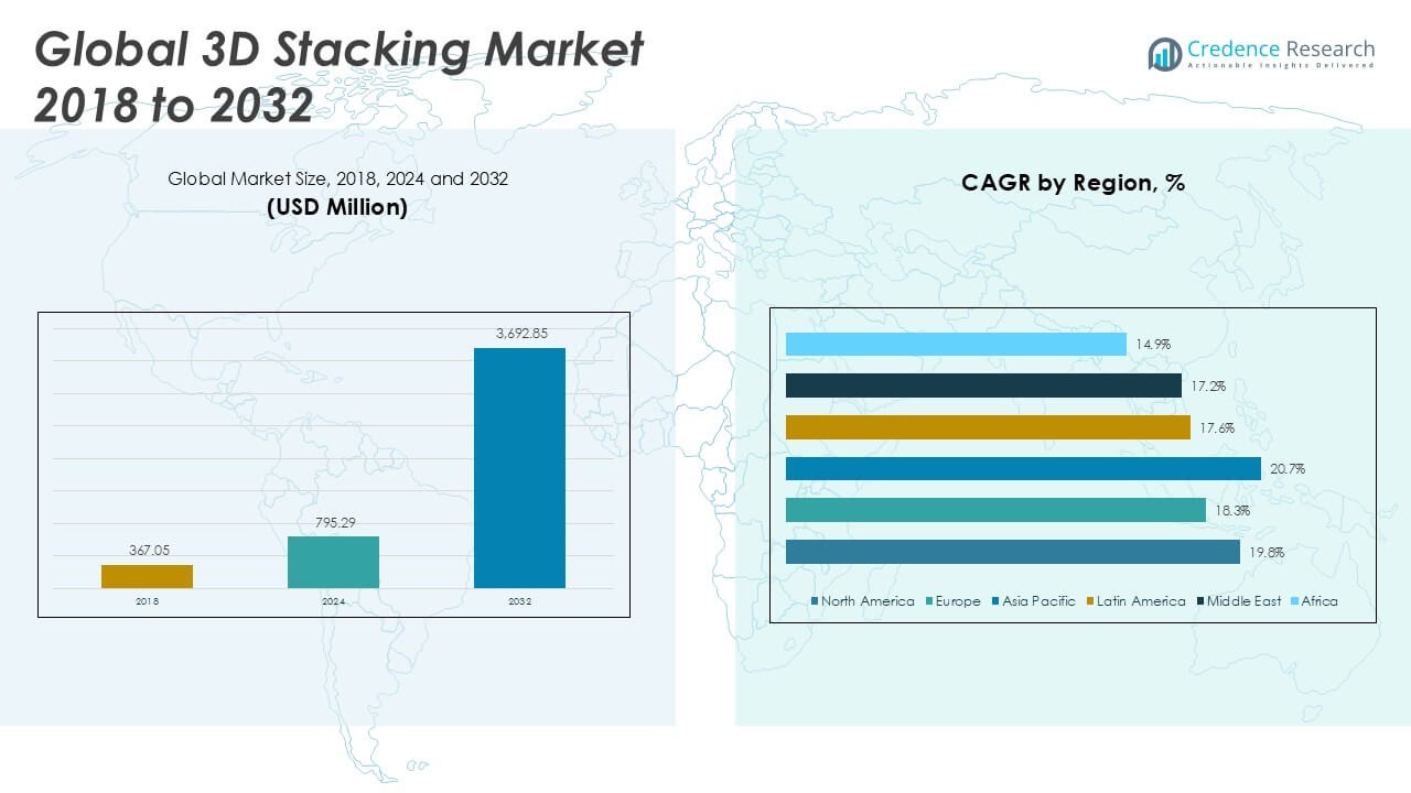
The 3D Stacking Market size was valued at USD 367.05 million in 2018, grew to USD 795.29 million in 2024, and is anticipated to reach USD 3,692.85 million by 2032, at a CAGR of 19.73% during the forecast period.
The 3D Stacking Market is driven by the growing demand for high-performance computing, energy-efficient electronics, and compact device architectures across industries such as consumer electronics, automotive, and data centers. As traditional 2D scaling reaches physical limitations, 3D stacking offers improved performance, reduced latency, and lower power consumption by enabling vertical integration of heterogeneous components. The rise of AI, IoT, and 5G technologies accelerates adoption, requiring faster data processing and greater memory bandwidth. Market trends include increasing investments in advanced packaging technologies, such as through-silicon vias (TSVs) and wafer-level stacking, to enhance chip functionality and reduce form factor. Leading semiconductor manufacturers are exploring hybrid bonding and chiplet-based designs to improve scalability and customization. Moreover, strategic partnerships and innovations in thermal management and interconnect solutions are shaping the competitive landscape. As end-user applications demand more efficient and compact electronic systems, the market continues to evolve toward greater integration and functional density.
The geographical landscape of the 3D Stacking Market shows strong presence across Asia Pacific, North America, and Europe, driven by rapid advancements in semiconductor manufacturing and rising demand for compact, high-performance devices. Asia Pacific leads in terms of adoption due to the dominance of chip fabrication hubs in China, Taiwan, South Korea, and Japan. North America follows closely with substantial investments in AI, data centers, and advanced packaging technologies, while Europe contributes through its focus on automotive electronics and industrial automation. Countries like the United States, China, and South Korea play pivotal roles in shaping global trends. Key players in the 3D Stacking Market include TSMC, which is a leader in semiconductor foundry services, Intel Corporation, known for its investment in heterogeneous integration and packaging technologies, and Samsung Electronics, recognized for innovations in memory and logic chip stacking. Amkor Technology also contributes with its advanced packaging solutions serving various verticals.
Access crucial information at unmatched prices!
Request your sample report today & start making informed decisions powered by Credence Research Inc.!
Download Sample
Market Insights
- The 3D Stacking Market was valued at USD 795.29 million in 2024 and is projected to reach USD 3,692.85 million by 2032, growing at a CAGR of 19.73% during the forecast period.
- The market is expanding rapidly due to increasing demand for compact, energy-efficient, and high-performance electronics across consumer devices, automotive, and data infrastructure.
- Integration of AI, 5G, and IoT technologies is pushing demand for faster data processing and high-bandwidth memory, accelerating adoption of 3D stacking in logic and memory applications.
- Key players such as TSMC, Samsung Electronics, Intel Corporation, and Amkor Technology are investing in advanced packaging methods and chiplet architectures to enhance performance and design flexibility.
- High manufacturing complexity, yield challenges, and thermal management issues act as major restraints, particularly in high-density and high-power applications.
- Asia Pacific leads the market in terms of growth and volume due to its strong semiconductor manufacturing base, followed by North America and Europe which contribute through R&D and technological adoption.
- Trends such as hybrid bonding, monolithic 3D integration, and government-backed semiconductor initiatives are shaping future innovations and commercial scalability.
Market Drivers
Surging Demand for High-Performance and Compact Electronic Devices Across Multiple Industries
The 3D Stacking Market is primarily driven by the rising need for high-performance and miniaturized electronic devices. Sectors such as consumer electronics, automotive, healthcare, and telecommunications are integrating smaller and more powerful components into their systems. This trend is pushing manufacturers to adopt 3D stacking technologies that offer improved speed, efficiency, and functional density. The ability to stack dies vertically helps overcome the physical scaling limits of traditional 2D integration, enabling better use of limited board space. Compact designs are critical for smartphones, wearables, and advanced driver assistance systems. The growing penetration of these devices supports the continuous expansion of the market.
- For instance, Apple’s A17 Pro chip, used in the iPhone 15 Pro, incorporates TSMC’s second-generation 3nm process with advanced stacking, achieving 19 billion transistors in a compact architecture.
Accelerated Growth in Artificial Intelligence, 5G, and Internet of Things Applications
The demand for faster data processing and real-time analytics in AI, 5G, and IoT ecosystems is fueling the adoption of 3D stacking solutions. These technologies require high memory bandwidth and energy-efficient data handling, which conventional packaging cannot deliver. 3D stacking offers closer interconnects between chips, reducing latency and improving communication speed. The market benefits from the shift toward edge computing, where localized data processing is crucial. It plays a central role in supporting the performance requirements of next-generation technologies. Continuous investment in AI-driven infrastructure strengthens the need for high-performance stacked architectures.
- For instance, NVIDIA’s H100 GPU integrates 80 billion transistors and connects to six HBM3 memory stacks using a 4096-bit interface, delivering 3.35 TB/s of memory bandwidth.
Increasing Limitations of Moore’s Law and Traditional Scaling Methods
With traditional semiconductor scaling approaching its physical limits, manufacturers are turning to 3D stacking to maintain performance improvements. It enables vertical chip integration without increasing the footprint, a significant advantage in space-constrained applications. This approach helps reduce signal path length, enhancing both speed and power efficiency. The 3D Stacking Market benefits from this transition by offering scalable solutions compatible with heterogeneous integration. Developers are leveraging this technology to combine memory, logic, and analog components in a single package. It is becoming an essential strategy for overcoming the diminishing returns of planar scaling.
Rising Investments in Advanced Packaging Technologies and Infrastructure
The market is gaining momentum due to increased investments in advanced packaging infrastructure, research, and development. Key semiconductor players are adopting through-silicon vias (TSVs), wafer-level packaging, and hybrid bonding to improve yield and performance. These innovations are enabling the production of cost-effective and reliable 3D ICs. Governments and private stakeholders are also supporting initiatives focused on next-generation chip manufacturing capabilities. It is benefiting from a well-established supply chain and global focus on semiconductor self-sufficiency. This funding landscape ensures a continuous pipeline of technological advancement and commercial deployment.
Market Trends
Adoption of Heterogeneous Integration and Chiplet-Based Architectures Gaining Ground
The 3D Stacking Market is witnessing a shift toward heterogeneous integration and chiplet-based designs to meet advanced performance requirements. Designers are breaking down complex system-on-chip (SoC) designs into smaller functional blocks, known as chiplets, which are then stacked or integrated in 3D configurations. This approach enhances modularity, flexibility, and reuse across different applications while reducing design complexity and cost. It supports mixed technology nodes in a single package, combining logic, memory, analog, and RF components effectively. Leading semiconductor firms are building open chiplet ecosystems to accelerate innovation and adoption. These developments are setting the foundation for scalable, high-performance computing solutions.
- For instance, AMD’s EPYC 9654 “Genoa” processor comprises 12 compute dies and one I/O die on a single substrate, delivering up to 96 cores and 192 threads.
Growing Integration of Through-Silicon Vias and Hybrid Bonding Techniques
Through-silicon vias (TSVs) and hybrid bonding methods are becoming central to the evolution of 3D stacking technologies. TSVs enable vertical electrical connections through the silicon substrate, drastically reducing interconnect length and power consumption. Hybrid bonding, which combines wafer-to-wafer and die-to-wafer techniques, offers stronger mechanical stability and better signal integrity. The 3D Stacking Market is expanding due to the improved reliability and performance these methods provide. Manufacturers are refining these technologies to achieve higher yields and lower production costs. The continuous enhancement of bonding techniques supports broader commercial viability.
- For instance, Intel’s Foveros Direct hybrid bonding technology achieves a bump pitch of 10 microns, enabling over 400 million interconnects per square millimeter between stacked dies.
Emphasis on Advanced Thermal Management and System Reliability Solutions
Thermal performance is a growing concern in vertically stacked architectures due to higher power density. The market is responding by investing in innovative thermal interface materials, microfluidic cooling systems, and advanced packaging designs. These solutions aim to distribute heat more efficiently and prevent performance degradation or component failure. The 3D Stacking Market is evolving through collaboration between packaging engineers, material scientists, and system designers. Companies are also deploying AI-driven thermal modeling to optimize stack configurations. This focus on reliability ensures long-term functionality in critical computing environments.
Expansion into AI Data Centers, Autonomous Vehicles, and 6G Infrastructure
Emerging applications in AI data centers, autonomous vehicles, and future 6G infrastructure are driving the need for advanced 3D stacking solutions. These use cases demand ultra-high bandwidth, low latency, and energy efficiency, all of which align with the core advantages of 3D integration. The market is experiencing growth through its alignment with these high-performance applications. Major industry players are aligning product development roadmaps to support evolving computational workloads. It is playing a strategic role in enabling next-generation digital infrastructure. These trends reflect a robust and future-oriented outlook for the market.
Market Challenges Analysis
High Manufacturing Complexity and Yield Management Constraints Impact Commercial Scalability
The 3D Stacking Market faces challenges related to the intricate manufacturing processes required for vertical integration. Techniques such as through-silicon vias (TSVs), wafer bonding, and die alignment demand precision and advanced equipment, which drive up production costs. Any misalignment or defect in one layer can compromise the performance of the entire stack, leading to significant yield loss. Manufacturers must invest heavily in quality control systems and cleanroom environments to ensure reliability. These constraints hinder the scalability of 3D stacking in cost-sensitive applications. It remains a significant barrier for mass production, particularly in industries with narrow profit margins.
Thermal Dissipation and Testing Complexity Limit Deployment in High-Power Applications
Effective heat management remains a persistent challenge in 3D stacking due to increased power density in compact spaces. Inadequate thermal dissipation can lead to overheating, affecting performance and reliability, especially in high-compute environments like AI servers or autonomous vehicle systems. Traditional cooling methods often fall short, requiring new materials and structural redesigns to manage temperature more efficiently. The 3D Stacking Market also encounters difficulties in post-assembly testing, where accessing internal layers for defect analysis is complex and time-consuming. It demands the development of advanced diagnostic tools and predictive models to ensure long-term stability. These factors slow the pace of adoption across broader applications.
Market Opportunities
Expansion of Edge Computing and AI Workloads Unlocks New Application Potential
The growing demand for localized processing in edge computing, AI inference engines, and real-time analytics presents a strong opportunity for the 3D Stacking Market. These applications require compact, high-performance, and energy-efficient hardware, which aligns with the core capabilities of 3D stacked architectures. It can enable faster data transfer, reduced latency, and better thermal efficiency in devices deployed at the edge. With smart cities, autonomous systems, and industrial IoT gaining momentum, manufacturers can develop targeted 3D solutions tailored for low-footprint, high-output environments. The ability to integrate logic, memory, and RF components in a single package makes this technology well-suited for next-generation edge devices. This demand shift supports innovation in design and packaging tailored for decentralized processing systems.
Government Funding and Semiconductor Nationalization Strategies Fuel Investment Prospects
Increased government initiatives supporting domestic semiconductor manufacturing present a favorable environment for the expansion of advanced packaging technologies. Countries such as the U.S., China, South Korea, and members of the EU are allocating substantial funds to establish resilient chip supply chains and reduce dependence on foreign sources. The 3D Stacking Market stands to benefit from this push, as nations prioritize advanced node capabilities and chiplet-based integration. It offers a strategic pathway to enhance national competitiveness in critical sectors like defense, aerospace, and AI. Startups and R&D institutions can secure funding for developing proprietary 3D stacking solutions under public-private collaboration models. This funding landscape accelerates commercialization and adoption across new industrial verticals.
Market Segmentation Analysis:
By Device Type:
Memory devices hold a dominant share in the 3D Stacking Market due to their critical role in high-performance computing and data storage applications. Stacking DRAM and NAND chips vertically increases density and improves bandwidth while reducing footprint. Logic ICs follow closely, driven by demand from AI accelerators, GPUs, and CPUs requiring integrated performance. Imaging and optoelectronics segments benefit from mobile phone cameras and advanced sensors, which need compact, efficient integration. MEMS/sensors are gaining adoption in automotive and medical devices, where space-saving and high-speed data processing are essential. LEDs and other devices present steady growth due to their use in compact lighting and display systems.
- For instance, Samsung’s 236-layer V-NAND offers 1 Tb (128 GB) per chip, supporting up to 2.4 GB/s read speeds and 2.0 GB/s write speeds in Gen 5 SSDs.
By Method:
Through-silicon vias (TSVs) dominate due to their maturity and wide adoption in memory and high-end logic devices. They provide efficient vertical connections and high signal integrity. Interposer-based stacking is preferred in heterogeneous integration, allowing different components to communicate through a silicon or organic interposer layer. Die-to-die bonding supports chiplet-based architecture and allows integration of various functional blocks, improving modularity and cost efficiency. Wafer-level stacking is expanding across consumer electronics and MEMS devices due to its scalability and lower production cost. Other methods, including hybrid models, contribute to meeting diverse packaging needs.
- For instance, TSMC’s CoWoS-L technology supports up to 12 HBM3e memory stacks delivering over 1.6 TB/s memory bandwidth in next-generation AI accelerators.
By Interconnecting Technology:
3D TSV continues to lead due to its reliability in large-scale manufacturing and proven performance in commercial memory products. It plays a vital role in the deployment of high-bandwidth memory (HBM) and AI accelerators. The 3D Stacking Market is also seeing rapid growth in 3D hybrid bonding, which provides improved alignment accuracy, mechanical strength, and electrical performance without using solder bumps. Monolithic 3D integration is emerging, offering potential for finer scaling by integrating layers during wafer fabrication. It remains in early development stages but holds promise for future chip design advancements across logic and memory integration.
Segments:
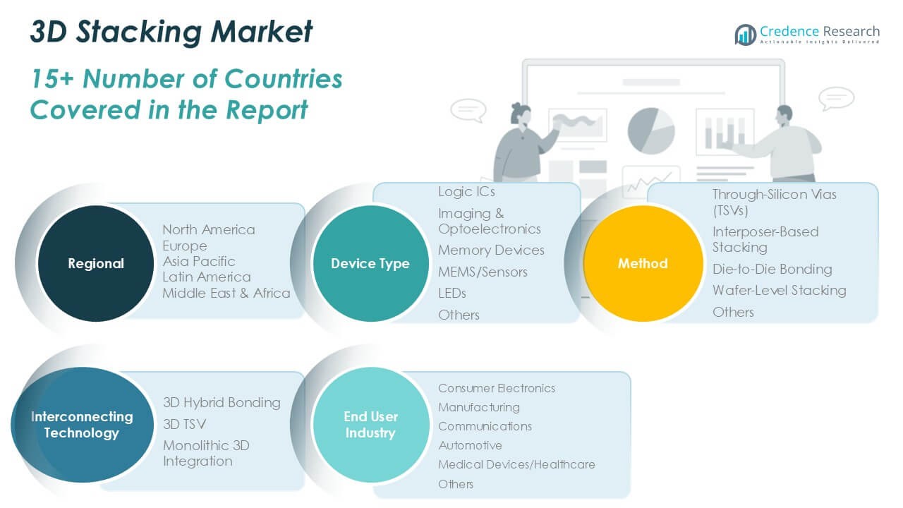
Based on Device Type:
- Logic ICs
- Imaging & Optoelectronics
- Memory Devices
- MEMS/Sensors
- LEDs
- Others
Based on Method:
- Through-Silicon Vias (TSVs)
- Interposer-Based Stacking
- Die-to-Die Bonding
- Wafer-Level Stacking
- Others
Based on Interconnecting Technology:
- 3D Hybrid Bonding
- 3D TSV
- Monolithic 3D Integration
Based on End User Industry:
- Consumer Electronics
- Manufacturing
- Communications
- Automotive
- Medical Devices/Healthcare
- Others
Based on the Geography:
- North America
- Europe
- UK
- France
- Germany
- Italy
- Spain
- Russia
- Belgium
- Netherlands
- Austria
- Sweden
- Poland
- Denmark
- Switzerland
- Rest of Europe
- Asia Pacific
- China
- Japan
- South Korea
- India
- Australia
- Thailand
- Indonesia
- Vietnam
- Malaysia
- Philippines
- Taiwan
- Rest of Asia Pacific
- Latin America
- Brazil
- Argentina
- Peru
- Chile
- Colombia
- Rest of Latin America
- Middle East
- UAE
- KSA
- Israel
- Turkey
- Iran
- Rest of Middle East
- Africa
- Egypt
- Nigeria
- Algeria
- Morocco
- Rest of Africa
Regional Analysis
North America 3D Stacking Market
North America 3D Stacking Market grew from USD 123.09 million in 2018 to USD 263.09 million in 2024 and is projected to reach USD 1,226.04 million by 2032, reflecting a compound annual growth rate (CAGR) of 19.8%. North America is holding a 33% market share. The United States leads the region with strong investments in AI, 5G, and advanced semiconductor packaging. Government support through initiatives like the CHIPS Act and strong R&D from players such as Intel and AMD contribute to sustained growth. Demand from data centers, consumer electronics, and automotive sectors supports adoption of 3D stacking. Canada is also emerging as a contributor, especially in medical technology and communications infrastructure.
Asia Pacific 3D Stacking Market
Asia Pacific 3D Stacking Market grew from USD 145.93 million in 2018 to USD 329.01 million in 2024 and is projected to reach USD 1,629.78 million by 2032, reflecting a CAGR of 20.7%. Asia Pacific holds the largest market share at 39%. China, Japan, South Korea, and Taiwan dominate regional growth due to their leadership in semiconductor manufacturing and advanced packaging. Countries in the region are investing in domestic chip production and 3D integration to secure supply chains. The growing electronics manufacturing ecosystem and strong consumer base drive demand. Strategic partnerships and innovations from firms like TSMC, Samsung, and Sony support technological progress across applications.
Europe 3D Stacking Market
Europe 3D Stacking Market grew from USD 68.44 million in 2018 to USD 140.15 million in 2024 and is projected to reach USD 591.68 million by 2032, with a CAGR of 18.3%. Europe accounts for 15% of the global market. Germany, France, and the Netherlands are key contributors, driven by automotive electronics, industrial automation, and imaging systems. The region focuses on energy efficiency and high-reliability systems, prompting adoption of advanced packaging. Public-private partnerships support semiconductor innovation and infrastructure. Companies are investing in AI processors and high-density memory integration to serve regional demand.
Latin America 3D Stacking Market
Latin America 3D Stacking Market grew from USD 15.16 million in 2018 to USD 32.38 million in 2024 and is projected to reach USD 130.55 million by 2032, registering a CAGR of 17.6%. Latin America holds a 4% market share. Brazil and Mexico lead the region, focusing on smart electronics and industrial IoT integration. Increasing investments in telecom and data infrastructure contribute to market expansion. Local production capabilities remain limited, but demand for advanced electronic components continues to grow. Governments are exploring policies to boost tech-sector competitiveness and digital transformation.
Middle East 3D Stacking Market
Middle East 3D Stacking Market grew from USD 10.44 million in 2018 to USD 20.72 million in 2024 and is projected to reach USD 81.43 million by 2032, reflecting a CAGR of 17.2%. The Middle East holds a 2% share of the global market. The UAE and Saudi Arabia are advancing in smart city initiatives and digital infrastructure development, driving demand for compact, high-performance computing solutions. Data center investments and AI-driven defense applications increase regional interest in 3D stacking technologies. Focus remains on importing advanced components, though efforts to build local capabilities are increasing.
Africa 3D Stacking Market
Africa 3D Stacking Market grew from USD 4.00 million in 2018 to USD 9.95 million in 2024 and is projected to reach USD 33.37 million by 2032, with a CAGR of 14.9%. Africa holds a 1% market share. South Africa leads adoption, followed by Nigeria and Kenya, where tech hubs and telecom expansion are creating modest but growing demand. The region faces infrastructure and investment constraints but shows potential in low-power, compact computing systems. Efforts to improve local R&D and digital literacy could open further opportunities for market penetration.
Key Player Analysis
- Medtronic
- BD
- Abbott Laboratories
- Braun Melsungen
- A&E Medical
- Edwards Lifesciences
- Oscor Inc.
- BioTrace Medical
- Teleflex Incorporated
- Osypka Medical GmbH
- LivaNova PLC
- Shree Pacetronix Ltd.
Competitive Analysis
The 3D Stacking Market is highly competitive, with key players including TSMC, Intel Corporation, Samsung Electronics, Amkor Technology, ASE Technology Holding Co., Ltd., SK Hynix Inc., and Micron Technology Inc. These companies drive market leadership through continuous innovation in advanced packaging technologies, including through-silicon vias (TSVs), hybrid bonding, and chiplet-based architectures. The competitive environment encourages continuous upgrades in packaging techniques to meet the evolving needs of sectors like AI, automotive electronics, and data centers. Firms differentiate themselves by offering scalable, cost-effective packaging solutions and by building strategic alliances across the semiconductor value chain. The ability to deliver higher bandwidth, lower power consumption, and improved thermal efficiency remains a key factor in gaining a competitive edge. Players are also expanding their global manufacturing footprints and leveraging government-backed initiatives to strengthen supply chain resilience. Competition centers on product reliability, customization, and time-to-market, shaping a dynamic and innovation-led market landscape.
Recent Developments
- In September 2024, Samsung is planning to start mass production of 3D stacked SoCs around 2026, which will be done with hybrid bonding and TC-NCF for greater performance improvement. Early test success with TC-NCF looks good, although yield-related problems are still in the offing for the 3nm process, which does not seem to be an easy challenge for the company.
- In June 2024, Samsung introduced its 3D HBM chip packaging service, enhancing data speeds by vertically stacking memory and processors. This method replaces traditional 2.5D packaging, aiming to strengthen its market position against competitors like TSMC.
- In June 2023, Cadence Design Systems, Inc. has expanded its collaboration with Samsung Foundry to accelerate 3D-IC design development for emerging technologies like hyperscale computing, 5G, AI, IoT, and mobile applications. This partnership enhances multi-die planning and implementation through reference flows and package design kits based on the Cadence Integrity 3D-IC platform, which uniquely integrates system planning, packaging, and system-level analysis.
- In February 2023, UMC (Taiwan) and Cadence (US) collaborated on 3D-IC Hybrid Bonding Reference Flow. This technology supports the integration across a broad range of technology nodes suitable for edge AI, image processing, and wireless communication applications. Cost-effectiveness and design reliability are the pillars of UMC’s hybrid bonding technologies, and this collaboration with Cadence provides mutual customers with both, helping them reap the benefits of 3D structures while also accelerating the time needed to complete their integrated designs.
Market Concentration & Characteristics
The 3D Stacking Market demonstrates moderate to high market concentration, with a few global players holding significant technological and production capabilities. It is characterized by strong integration of semiconductor design, packaging, and manufacturing expertise. The market relies heavily on advanced infrastructure, precision engineering, and R&D-intensive processes, making entry difficult for new participants. It favors companies with established foundry operations, proprietary bonding methods, and high-volume production capacity. Demand centers around sectors requiring high-performance, energy-efficient, and space-saving components, such as AI, HPC, consumer electronics, and automotive systems. The market operates under high technological complexity, with long development cycles and strict quality control standards. It shows strong alignment with the evolution of chiplet architectures and heterogeneous integration trends, which shape its competitive dynamics.
Shape Your Report to Specific Countries or Regions & Enjoy 30% Off!
Report Coverage
The research report offers an in-depth analysis based on Device Type, Method, Interconnecting Technology, End User Industry and Geography. It details leading market players, providing an overview of their business, product offerings, investments, revenue streams, and key applications. Additionally, the report includes insights into the competitive environment, SWOT analysis, current market trends, as well as the primary drivers and constraints. Furthermore, it discusses various factors that have driven market expansion in recent years. The report also explores market dynamics, regulatory scenarios, and technological advancements that are shaping the industry. It assesses the impact of external factors and global economic changes on market growth. Lastly, it provides strategic recommendations for new entrants and established companies to navigate the complexities of the market.
Future Outlook
- The 3D stacking market is poised to expand due to growing demand for high-performance and compact electronic devices.
- Increasing adoption of AI, IoT, and 5G technologies is accelerating the need for efficient and dense chip architectures.
- Advancements in semiconductor fabrication techniques are enabling more cost-effective 3D stacking solutions.
- The market will benefit from rising demand for high-bandwidth memory in data centers and gaming applications.
- Smartphone and wearable manufacturers are integrating 3D stacked chips to enhance performance and reduce size.
- Growing interest in heterogeneous integration is driving the adoption of 3D stacking across various sectors.
- The automotive industry is adopting 3D ICs for enhanced processing power in electric and autonomous vehicles.
- Continued R&D investments by major chipmakers are expected to lead to innovations in interconnect and thermal management.
- Asia-Pacific will remain a major hub for 3D stacking due to strong semiconductor manufacturing capabilities.
- Collaborative efforts among foundries, OSATs, and design firms are fostering ecosystem development for 3D integration.


