Market overview
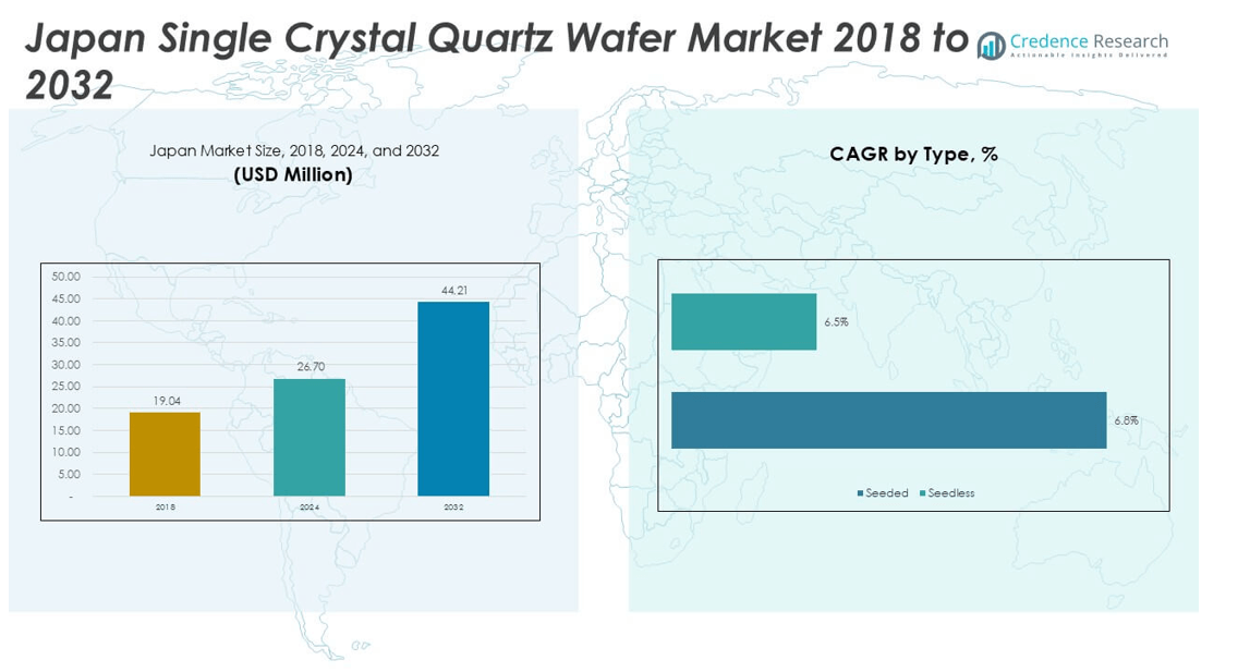
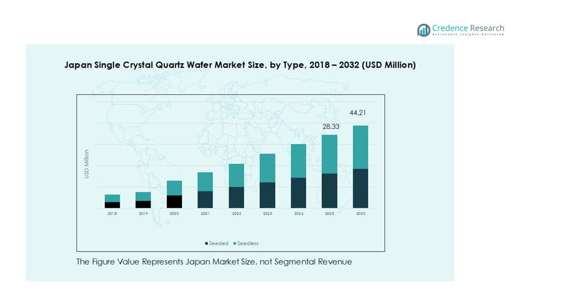
The Japan single crystal quartz wafer market size was valued at USD 19.04 million in 2018, reaching USD 26.70 million in 2024, and is anticipated to reach USD 44.21 .million by 2032, at a CAGR of 6.3% during the forecast period.
| REPORT ATTRIBUTE |
DETAILS |
| Historical Period |
2020-2023 |
| Base Year |
2024 |
| Forecast Period |
2025-2032 |
| Japan Single Crystal Quartz Wafer Market Size 2025 |
USD 26.70 million |
| Japan Single Crystal Quartz Wafer Market, CAGR |
6.3% |
| Japan Single Crystal Quartz Wafer Market Size 2032 |
USD 44.21 million |
The Japan single crystal quartz wafer market is led by key players including Corning Incorporated, Ferrotec Global, NIHON DEMPA KOGYO CO., LTD., MTI Corporation, and Wafer Technology Ltd. These companies maintain strong positions through advanced crystal growth technologies, high-purity wafer production, and long-standing collaborations with semiconductor and electronics manufacturers. Corning and Ferrotec lead with established global networks, while NIHON DEMPA KOGYO leverages domestic expertise in precision materials. MTI and Wafer Technology focus on research-driven and specialty wafer solutions. Regionally, the Kanto region holds the largest market share at 34%, supported by its concentration of semiconductor fabs and R&D centers. Kansai follows with 22% share, benefiting from its electronics and MEMS manufacturing ecosystem. Together, these regions account for over half of the national market, reflecting their dominance in Japan’s semiconductor value chain.
Market Insights
- The Japan single crystal quartz wafer market was valued at USD 26.70 million in 2024 and is projected to reach USD 44.21 million by 2032, expanding at a CAGR of 6.3%.
- Rising semiconductor demand is the primary driver, as quartz wafers ensure high purity and dimensional stability in lithography, MEMS devices, and IC packaging.
- Market trends highlight the shift toward larger-diameter wafers above 8 inches and growing adoption in MEMS and biotechnology applications, supported by Japan’s strong electronics ecosystem.
- Competition features leading companies such as Corning Incorporated, Ferrotec Global, and NIHON DEMPA KOGYO CO., LTD., focusing on innovation, reliability, and expanding wafer production to meet advanced technology requirements.
- Regionally, the Kanto region leads with 34% share, followed by Kansai at 22%, while by application, semiconductors dominate with 46% share, underscoring Japan’s strong position in electronics and advanced materials integration.
Access crucial information at unmatched prices!
Request your sample report today & start making informed decisions powered by Credence Research Inc.!
Download Sample
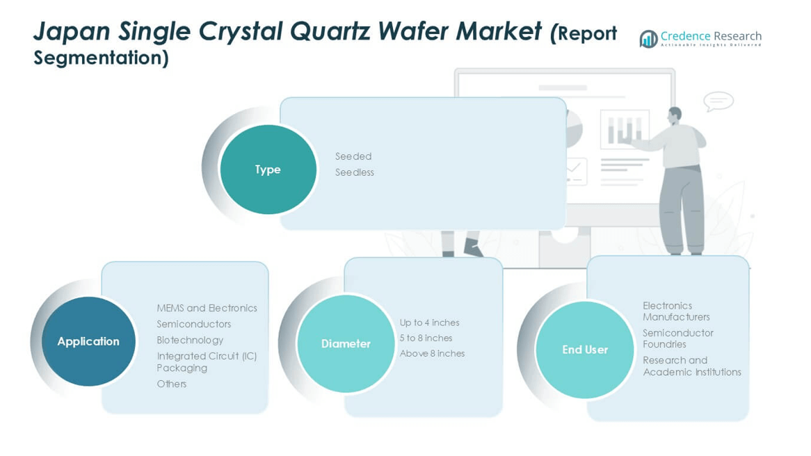
Market Segmentation Analysis:
By Type
The Japan single crystal quartz wafer market by type is segmented into seeded and seedless. Seeded wafers dominated the segment in 2024, accounting for nearly 65% share, due to their precise crystalline orientation and consistency, which are critical in semiconductor and MEMS manufacturing. Their reliability in delivering uniform lattice structures supports device performance and reduces defect rates. Increasing demand for high-frequency devices and advanced microelectronics strengthens the preference for seeded wafers. Seedless wafers, while growing, are mainly used in applications where production flexibility and lower costs are prioritized.
- For instance, Shin-Etsu Chemical, a world leader in the field, manufactures ultra-high-purity silicon wafers used for producing integrated circuits. The industry standard for high-volume manufacturing is the 300 mm wafer, though the company also supplies legacy 200 mm wafers for specialized applications.
By Diameter
In terms of diameter, the market is divided into up to 4 inches, 5 to 8 inches, and above 8 inches. The 5 to 8 inches segment held the largest share of about 58% in 2024, driven by its compatibility with mainstream semiconductor fabrication processes. These wafers provide an optimal balance between cost efficiency and technological performance, making them widely adopted by leading fabs. The rising investment in MEMS sensors and RF devices fuels demand for mid-sized wafers. Meanwhile, above 8 inches wafers are gaining attention as advanced nodes push for larger-scale integration.
- For instance, Sony Semiconductor manufactures CMOS image sensors on 12-inch wafers for next-generation camera modules, achieving pixel counts in excess of 100 megapixels for individual sensors.
By Application
Based on application, the market includes MEMS and electronics, semiconductors, biotechnology, integrated circuit (IC) packaging, and others. The semiconductor segment led with a 46% share in 2024, as quartz wafers are essential in photomasks, lithography, and wafer processing. Their high purity and stability ensure precision in microchip production, aligning with Japan’s strong semiconductor ecosystem. Growth in 5G, automotive electronics, and AI-driven devices drives this demand further. MEMS and electronics also show robust growth, supported by rising sensor applications in consumer devices and automotive technologies, while biotechnology uses are emerging in niche fields like biosensors.
Key Growth Drivers
Rising Demand in Semiconductor Industry
The semiconductor sector remains the strongest driver of Japan’s single crystal quartz wafer market. Quartz wafers are crucial in lithography, etching, and photomask applications, ensuring dimensional stability and high purity. With Japan’s leadership in semiconductor production for memory chips, automotive electronics, and logic devices, demand continues to rise. The expansion of 5G infrastructure, artificial intelligence chips, and consumer electronics amplifies wafer consumption. Domestic manufacturers are investing in advanced fabrication plants, boosting wafer utilization. Government initiatives supporting semiconductor self-sufficiency further increase adoption, positioning quartz wafers as a backbone material for sustaining Japan’s semiconductor ecosystem.
- For instance, Kioxia manufactures a significant number of 300 mm NAND flash wafers monthly in its Yokkaichi plant, each of which relies on high-purity quartz for the photolithography stages of its production process.
Technological Advancements in MEMS and Electronics
Growing adoption of MEMS devices, such as sensors, microphones, and RF components, drives market growth. Quartz wafers provide mechanical stability and frequency precision, making them integral for MEMS manufacturing. The automotive sector increasingly uses MEMS sensors for safety, autonomous driving, and infotainment, while smartphones and wearables rely heavily on MEMS microphones and accelerometers. Japanese firms are advancing quartz wafer processing to meet the precision demands of IoT-enabled electronics. This technological shift is strengthening the market, as MEMS applications diversify into healthcare monitoring, industrial automation, and defense systems, accelerating the demand for reliable single crystal quartz wafers.
- For instance, TDK InvenSense integrates quartz-based MEMS gyroscopes with accuracy below 0.05°/s, tailored for drones and robotics.
Expanding Applications in Biotechnology
Biotechnology has emerged as a promising driver for quartz wafers in Japan. Their chemical stability, biocompatibility, and optical clarity make them suitable for biosensors, lab-on-chip platforms, and diagnostic devices. Japan’s growing focus on advanced healthcare, aging population, and precision diagnostics increases adoption of such technologies. Research institutes and startups are exploring quartz wafers for DNA sequencing, protein analysis, and microfluidic applications, supporting innovation in life sciences. The integration of biotechnology with electronics, known as bio-MEMS, further enhances market prospects. This expansion into healthcare applications creates a new revenue stream for quartz wafer manufacturers, broadening their growth opportunities.
Key Trends & Opportunities
Shift Toward Larger Diameter Wafers
The industry is moving toward larger wafer diameters, especially above 8 inches, to increase efficiency and reduce per-chip costs. While 5 to 8 inches currently dominate, semiconductor scaling and advanced electronics demand more integration capacity. Japan’s push toward miniaturization in consumer electronics and AI processors fuels this trend. Larger wafers enable higher yields per batch, making them attractive for advanced fabs. The opportunity lies in R&D investment and scaling production capabilities for large-diameter quartz wafers. As Japanese firms compete globally, larger wafers will support next-generation chip production, particularly for AI accelerators, automotive ADAS, and 6G communication systems.
- For instance, Sony Semiconductor manufactures 300 mm (12-inch) wafers for CMOS image sensors at its Kumamoto plant, with yields exceeding 90% for devices exceeding 100 million pixels per wafer
Integration of IoT and Smart Devices
The rapid penetration of IoT and connected devices creates a significant opportunity for quartz wafer adoption. MEMS-based sensors, powered by quartz stability, are critical for IoT ecosystems across consumer, industrial, and healthcare applications. Japan’s smart city projects, expanding 5G coverage, and automotive digitization amplify the demand for precision components. Quartz wafers provide long-term reliability, making them ideal for continuous monitoring devices. The opportunity extends to wearable healthcare, industrial automation, and logistics, where IoT adoption is accelerating. This integration trend encourages local manufacturers to innovate wafer processing technologies and strengthen supply chains for smart electronics production.
Key Challenges
High Production Costs and Complexity
Manufacturing single crystal quartz wafers involves complex processes, including precise crystal growth, orientation, and defect-free slicing. These steps increase production costs compared to other substrates like silicon. Japanese companies face challenges in maintaining cost competitiveness against global suppliers, particularly from regions with lower labor and energy costs. The high capital investment required for advanced equipment further strains small and medium enterprises. Rising energy prices also impact wafer manufacturing expenses. Unless efficiency improvements and economies of scale are achieved, high costs may limit wider adoption of quartz wafers in applications beyond premium electronics and semiconductors.
Supply Chain Constraints and Import Dependence
Japan relies on a steady supply of high-purity quartz raw materials, which are not abundantly available domestically. This dependence on imports exposes the industry to price volatility, geopolitical risks, and shipping disruptions. Global supply chain challenges, such as semiconductor shortages and raw material scarcity, have highlighted the vulnerability of wafer manufacturers. The limited number of suppliers for ultra-pure quartz further amplifies risks, as disruptions can halt production lines. Addressing these constraints requires diversification of sourcing, investment in recycling technologies, and collaboration with domestic mineral processors. Without supply chain resilience, the industry may struggle to meet rising demand.
Regional Analysis
Kanto Region
The Kanto region dominated the Japan single crystal quartz wafer market in 2024 with a 34% share. The region’s leadership stems from Tokyo and surrounding prefectures being hubs for semiconductor and electronics manufacturing. Major fabs and R&D centers located here drive demand for high-purity quartz wafers used in photomasks, MEMS devices, and IC packaging. Kanto also benefits from strong government and private investment in advanced semiconductor infrastructure. Expanding applications in 5G, automotive electronics, and consumer devices further strengthen its dominance, making Kanto the central growth engine for the country’s quartz wafer market.
Kansai Region
Kansai accounted for a 22% share of the market in 2024, supported by its strong base in electronic component manufacturing and materials innovation. Osaka and Kyoto host key companies specializing in semiconductor equipment and MEMS technologies, fueling demand for quartz wafers. The region’s universities and research institutes actively collaborate with industry, promoting technology transfer and wafer innovation. Rising adoption of MEMS sensors in automotive and consumer devices accelerates wafer consumption. Kansai’s established ecosystem of electronics manufacturers ensures steady market expansion, positioning the region as a key secondary hub after Kanto.
Chubu Region
The Chubu region held a 16% share in 2024, driven by its automotive industry and growing adoption of semiconductor technologies. With Nagoya as a manufacturing hub, the region increasingly incorporates quartz wafers in automotive electronics, MEMS sensors, and integrated circuits. Demand for precision electronics in autonomous vehicles and EVs boosts wafer adoption. Chubu’s industrial clusters provide opportunities for quartz wafer integration into advanced electronics, supported by strong collaborations between automakers and technology suppliers. Although smaller than Kanto and Kansai, Chubu is emerging as a significant growth contributor in Japan’s quartz wafer market.
Kyushu and Okinawa Region
Kyushu and Okinawa represented 12% of the market share in 2024, reflecting the region’s growing importance as Japan’s “Silicon Island.” Kyushu hosts major semiconductor fabs and foundries, which drive wafer demand for chip production and MEMS applications. Local governments actively support semiconductor investment, enhancing infrastructure and workforce availability. Quartz wafers are used extensively in photolithography and IC packaging within the region’s fabs. While Okinawa’s role is limited, Kyushu’s established semiconductor ecosystem ensures consistent growth, supported by its strategic focus on meeting domestic and global demand for high-performance semiconductor components.
Hokkaido and Tohoku Region
The Hokkaido and Tohoku region accounted for 9% share in 2024, mainly driven by investments in advanced electronics and government-supported semiconductor projects. Tohoku, in particular, is home to several R&D centers focusing on photonics and microelectronics, where quartz wafers are essential. Rising adoption of MEMS sensors for industrial and healthcare applications strengthens demand. While the market size remains smaller than in Kanto or Kansai, the region is attracting attention due to its research-driven ecosystem. Expansion of technology parks and government incentives is expected to gradually increase its contribution to the national quartz wafer market.
Chugoku and Shikoku Region
The Chugoku and Shikoku region held a 7% market share in 2024, making it the smallest contributor among all regions. The market here is primarily driven by niche applications in industrial electronics and smaller semiconductor-related businesses. While it lacks large-scale fabs, the region benefits from regional R&D initiatives and localized demand for specialty electronics. Shikoku’s focus on precision components and Chugoku’s industrial base support modest wafer adoption. Despite its limited size, the region offers potential growth opportunities through targeted collaborations and gradual integration of quartz wafers into emerging electronic and MEMS applications.
Market Segmentations:
By Type
By Diameter
- Up to 4 inches
- 5 to 8 inches
- Above 8 inches
By Application
- MEMS and Electronics
- Semiconductors
- Biotechnology
- Integrated Circuit (IC) Packaging
- Others
By End User
- Electronics Manufacturers
- Semiconductor Foundries
- Research and Academic Institutions
By Geography
- Kanto Region
- Kansai Region
- Chubu Region
- Kyushu and Okinawa Region
- Hokkaido and Tohoku Region
- Chugoku and Shikoku Region
Competitive Landscape
The competitive landscape of the Japan single crystal quartz wafer market is characterized by a mix of global leaders and regional specialists. Companies such as Corning Incorporated, Ferrotec Global, and NIHON DEMPA KOGYO CO., LTD. dominate with strong expertise in materials science and semiconductor applications. These firms leverage advanced manufacturing capabilities, high-purity quartz processing, and long-term partnerships with semiconductor fabs to secure market leadership. Emerging players like Vritra Technologies, MSE Supplies Inc., and UniversityWafer, Inc. target niche markets, offering customized wafer solutions for research and specialty electronics. Local companies emphasize reliability and technical collaboration, while global suppliers invest heavily in R&D to meet rising demand from 5G, automotive electronics, and MEMS applications. Strategic initiatives include product portfolio expansion, capacity upgrades, and partnerships with Japanese fabs to strengthen supply chains. Overall, competition is intensifying, with innovation, cost efficiency, and consistency in wafer quality serving as key differentiators for long-term success.
Shape Your Report to Specific Countries or Regions & Enjoy 30% Off!
Key Player Analysis
- Wafer Technology Ltd.
- Semiconductor Wafer, Inc.
- MTI Corporation
- Corning Incorporated
- Vritra Technologies
- Ferrotec Global
- MicroChemicals GmbH
- NIHON DEMPA KOGYO CO., LTD.
- MSE Supplies Inc.
- UniversityWafer, Inc.
- Other Key Players
Recent Developments
- In July 2025, Xiamen Powerway (PAM-XIAMEN) remains an active supplier of single crystal quartz wafers, specializing in X-cut, Y-cut, Z-cut, and ST-cut orientations up to 3-inch diameters.
- In July 2025, NDK highlighted its advancement in mass-producing high-uniformity quartz crystals using proprietary technologies. Their latest offering includes synthetic quartz wafers with AT-cut and tuning fork wafers, and a development plan for larger 6-inch wafers to cater to growing SAW device demand and frequency control in next-gen electronics.
- In August 2024, NDK (NIHON DEMPA KOGYO CO., LTD.) showcased its synthetic quartz crystals and quartz wafers for timing and optical applications at electronica India 2024, participating through a distributor’s booth at the trade fair.
Report Coverage
The research report offers an in-depth analysis based on Type, Diameter, Application, End-User and Geography. It details leading market players, providing an overview of their business, product offerings, investments, revenue streams, and key applications. Additionally, the report includes insights into the competitive environment, SWOT analysis, current market trends, as well as the primary drivers and constraints. Furthermore, it discusses various factors that have driven market expansion in recent years. The report also explores market dynamics, regulatory scenarios, and technological advancements that are shaping the industry. It assesses the impact of external factors and global economic changes on market growth. Lastly, it provides strategic recommendations for new entrants and established companies to navigate the complexities of the market.
Future Outlook
- The market will expand steadily with rising demand from semiconductor manufacturing.
- Growth in MEMS and sensor applications will support wider adoption of quartz wafers.
- Larger-diameter wafers above 8 inches will gain momentum to meet advanced chip needs.
- Biotechnology will emerge as a promising segment using quartz wafers in biosensors and lab-on-chip devices.
- Kanto and Kansai will continue to dominate, driven by semiconductor fabs and R&D centers.
- Domestic players will strengthen their supply chains to reduce reliance on imported raw materials.
- Technological advancements in wafer processing will improve efficiency and lower defect rates.
- Strategic partnerships between global suppliers and Japanese fabs will increase market competitiveness.
- Rising automotive electronics and EV adoption will drive new applications for quartz wafers.
- Sustainability and recycling of quartz materials will gain importance in the long-term market strategy.


