Market Overview
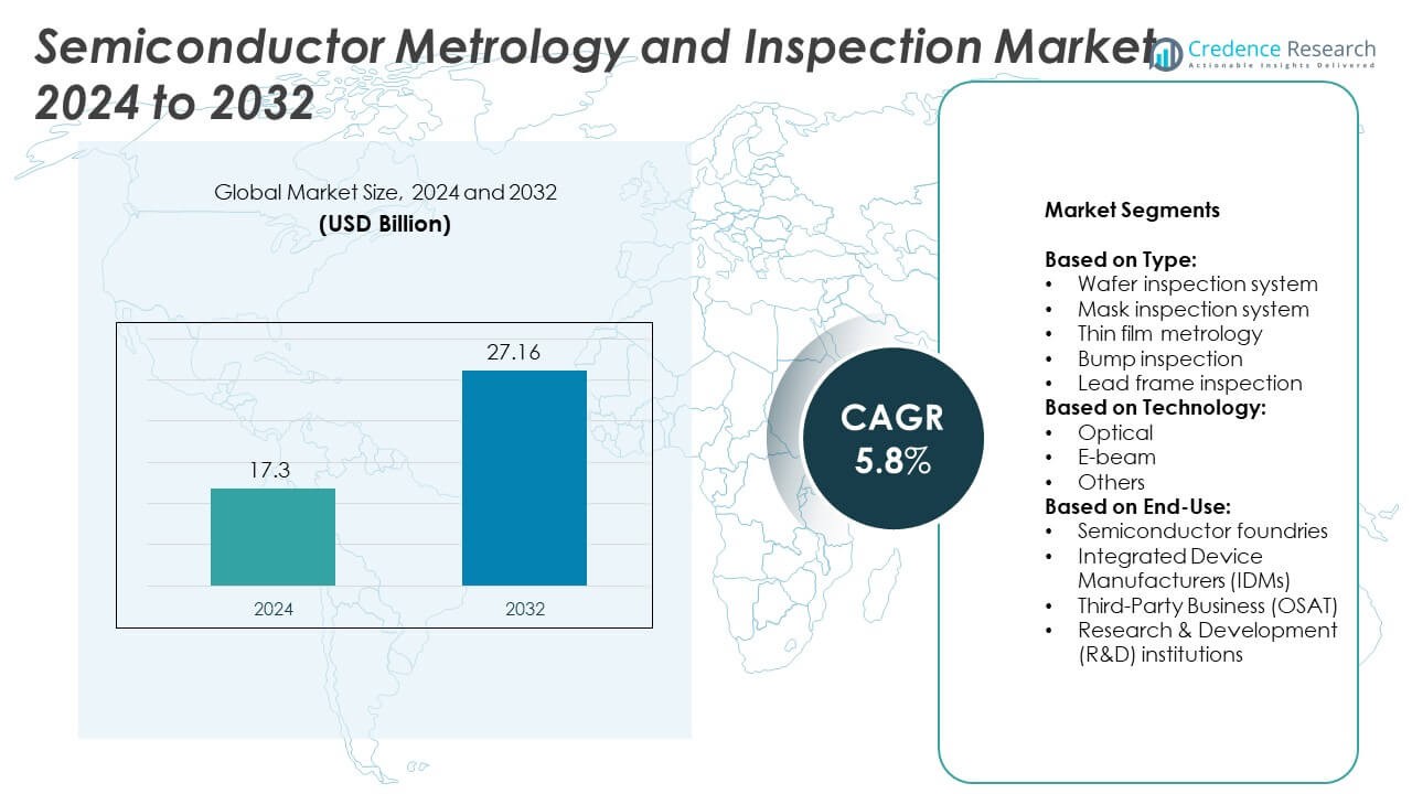
Semiconductor Metrology and Inspection Market size was valued at USD 17.3 billion in 2024 and is anticipated to reach USD 27.16 billion by 2032, growing at a CAGR of 5.8% during the forecast period.
| REPORT ATTRIBUTE |
DETAILS |
| Historical Period |
2020-2023 |
| Base Year |
2024 |
| Forecast Period |
2025-2032 |
| Semiconductor Metrology and Inspection Market Size 2024 |
USD 17.3 Billion |
| Semiconductor Metrology and Inspection Market, CAGR |
5.8% |
| Semiconductor Metrology and Inspection Market Size 2032 |
USD 27.16 Billion |
The Semiconductor Metrology and Inspection market grows due to rising demand for advanced semiconductor nodes, AI, IoT, 5G, and automotive applications. It benefits from adoption of high-precision wafer, mask, and thin film inspection systems. Manufacturers prioritize automation, inline inspection, and e-beam technologies to improve yield and reduce defects. Increasing investments by foundries, IDMs, and R&D institutions drive innovation in optical and AI-based solutions. Continuous process optimization and focus on quality control further strengthen market expansion.
North America leads the Semiconductor Metrology and Inspection market with advanced semiconductor infrastructure and strong R&D support. Europe follows with mature manufacturing ecosystems in Germany, France, and the Netherlands, emphasizing precision and compliance. Asia-Pacific grows rapidly due to expanding foundries in China, Taiwan, South Korea, and Japan, driven by high-volume production and emerging technologies. Key players, including KLA Corporation, Applied Materials, Inc., ASML, and Onto Innovation, focus on innovative inspection and metrology solutions, automation, and AI-based defect detection to meet diverse regional demands and advanced semiconductor requirements.
Access crucial information at unmatched prices!
Request your sample report today & start making informed decisions powered by Credence Research Inc.!
Download Sample
Market Insights
- The Semiconductor Metrology and Inspection market was valued at USD 17.3 billion in 2024 and is projected to reach USD 27.16 billion by 2032, growing at a CAGR of 5.8%.
- Growth is driven by increasing demand for advanced nodes, high-precision inspection, automation, and AI-enabled defect detection.
- Trends include adoption of optical and e-beam technologies, inline inspection, data analytics, and smart manufacturing integration.
- Key players like KLA Corporation, Applied Materials, Inc., ASML, Camtek, Onto Innovation, and Hitachi High-Tech Corporation focus on technological innovation and global expansion.
- Market restraints involve high equipment costs, limited skilled workforce, and challenges in adopting advanced metrology in emerging regions.
- North America leads with advanced infrastructure and strong R&D support, followed by Europe with mature manufacturing ecosystems.
- Asia-Pacific shows rapid growth due to expanding foundries, high production volumes, and government support for semiconductor manufacturing initiatives.
Market Drivers
Rising Demand for Advanced Semiconductor Devices Driving Market Expansion
The Semiconductor Metrology and Inspection market experiences strong growth due to increasing demand for advanced semiconductor devices. Miniaturization of chips and higher transistor densities require precise measurement and defect detection throughout manufacturing. It ensures product reliability and performance, reducing yield losses and production costs. Consumer electronics, automotive electronics, and high-performance computing drive continuous investment in metrology and inspection tools. Companies adopt sophisticated optical, electron, and X-ray-based inspection systems to meet stringent quality standards. Strong collaboration between semiconductor manufacturers and equipment providers enhances process control and innovation. It reinforces the market’s role in supporting next-generation semiconductor technologies.
- For instance, KLA Corporation provides automated optical inspection systems to wafer fabs in Taiwan and other semiconductor manufacturing hubs globally. KLA’s technology has been capable of defect detection below 45 nm for many years, as evidenced by product announcements dating back to 2007
Integration of Emerging Technologies Accelerating Efficiency in Semiconductor Manufacturing
Emerging technologies such as AI, machine learning, and automation enhance metrology and inspection efficiency. The Semiconductor Metrology and Inspection market benefits from faster defect detection, predictive maintenance, and improved throughput. It enables manufacturers to reduce downtime and optimize production processes while maintaining high accuracy. Advanced imaging and sensor integration allow detailed analysis of wafer surfaces and critical layers. Industrial adoption of smart manufacturing solutions supports real-time process monitoring and data-driven decision-making. This integration strengthens quality control and accelerates the development of smaller and more complex semiconductor nodes. It positions the market as essential in modern semiconductor fabrication.
- For instance, Applied Materials the company’s SEMVision eBeam review system is integrated with the Enlight optical wafer inspection system to quickly classify yield-killing defects. This integration supports high-volume manufacturing, helping chipmakers ramp production for devices with advanced geometries (sub-10 nm)
Expansion of 5G, IoT, and AI Applications Fueling Equipment Demand
The rapid deployment of 5G networks, IoT devices, and AI systems increases the need for reliable semiconductors. It drives investments in high-precision metrology and inspection tools to meet stringent performance and reliability standards. Semiconductor manufacturers deploy equipment capable of detecting nanoscale defects in advanced nodes. The Semiconductor Metrology and Inspection market grows with demand from telecommunications, automotive, and data center sectors. Manufacturers focus on improving yield and reducing scrap through precise measurements. It strengthens the adoption of automated and non-contact inspection technologies. Rising application diversity supports long-term market growth.
Stringent Quality Standards and Regulatory Compliance Strengthening Market Growth
Regulatory compliance and quality standards compel manufacturers to adopt advanced metrology and inspection solutions. It ensures defect-free production and adherence to international semiconductor standards. The Semiconductor Metrology and Inspection market benefits from tools that monitor critical parameters and maintain process consistency. Companies invest in inline and offline inspection systems for high-volume production environments. Traceability and documentation enhance accountability and product certification. It supports sustainability initiatives by reducing waste and improving material utilization. Strict quality requirements reinforce the market’s critical role in semiconductor manufacturing.
Market Trends
Adoption of High-Resolution and Multi-Dimensional Metrology Solutions Shaping Market Dynamics
The Semiconductor Metrology and Inspection market shows strong adoption of high-resolution and multi-dimensional metrology solutions. Manufacturers deploy advanced optical, electron, and X-ray systems to detect defects and measure critical dimensions at nanometer scales. It allows precise analysis of complex semiconductor structures and supports next-generation chip development. Equipment vendors focus on improving throughput while maintaining measurement accuracy. Integration of inline and offline inspection capabilities ensures comprehensive process control. The trend enhances yield management and reduces rework costs. It positions metrology tools as essential in modern semiconductor fabrication.
- For instance, in 2023, ASML shipped 53 EUV systems, demonstrating the scale of its deployment. The company’s technology has enabled significant improvements in accuracy and speed; in one documented case, the application of machine learning techniques improved overlay accuracy by a factor of two and significantly reduced the time needed for analysis
Shift Towards Automation and Artificial Intelligence Enhancing Manufacturing Precision
Automation and artificial intelligence increasingly influence the Semiconductor Metrology and Inspection market. It enables predictive analysis, faster defect identification, and real-time process adjustments. Semiconductor manufacturers implement AI-based algorithms to optimize measurement accuracy and reduce human intervention. Robotic handling and automated inspection stations increase throughput and operational efficiency. The trend supports high-volume production while maintaining consistent quality standards. Equipment providers focus on combining smart software with hardware innovations. It reinforces the market’s role in supporting complex and miniaturized semiconductor nodes.
- For instance, TEL has developed and patented systems that use machine learning to optimize plasma processes and improve defect detection. While TEL has a significant and large-scale global deployment of its equipment, including its plasma etch systems, verifiable public information does not confirm a specific number such as “over 1,500” systems delivered.
Integration of Data Analytics and Digital Twin Technology Driving Operational Insights
The Semiconductor Metrology and Inspection market benefits from data analytics and digital twin technology adoption. It provides manufacturers with actionable insights into process performance and equipment health. Advanced analytics support early detection of anomalies and process deviations, improving yield and reducing defects. Digital twins simulate wafer processes to optimize metrology strategies before physical implementation. Manufacturers use predictive modeling to enhance decision-making and reduce downtime. The trend enables continuous improvement in production efficiency and product reliability. It strengthens the market’s relevance in high-precision semiconductor manufacturing.
Demand for Non-Destructive and Inline Inspection Solutions Expanding Market Applications
Non-destructive and inline inspection solutions gain traction in the Semiconductor Metrology and Inspection market. It allows manufacturers to monitor wafers and devices without interrupting production. Inline tools detect defects early, reducing scrap and improving overall equipment efficiency. The market sees increased adoption of optical scatterometry, atomic force microscopy, and advanced X-ray inspection systems. Companies prioritize solutions that offer high speed, accuracy, and automation compatibility. It supports diverse applications across memory, logic, and advanced packaging technologies. Growing demand reinforces the market’s strategic importance in semiconductor fabrication.
Market Challenges Analysis
High Costs and Complex Integration of Advanced Metrology and Inspection Equipment Limiting Adoption
The Semiconductor Metrology and Inspection market faces challenges from the high costs of advanced measurement and inspection equipment. It requires significant capital investment, which can strain budgets, especially for smaller semiconductor manufacturers. Complex integration into existing production lines demands specialized expertise and extended setup time. Equipment maintenance and calibration add further operational expenses. Rapid technological evolution forces frequent upgrades to maintain competitiveness. It may delay adoption of new systems despite their potential to improve yield and accuracy. Vendors focus on modular designs and scalable solutions to mitigate these barriers.
Rapid Technology Evolution and Miniaturization Creating Operational and Analytical Challenges
Rapid semiconductor miniaturization and technological innovation present operational difficulties in the Semiconductor Metrology and Inspection market. It demands tools capable of detecting defects at sub-nanometer scales with high precision. Manufacturers struggle to keep pace with smaller nodes and complex 3D architectures. Limited standardization across advanced technologies complicates measurement and data interpretation. Training personnel and maintaining skilled teams remain critical for effective utilization. It increases pressure on companies to balance accuracy, throughput, and cost efficiency. These challenges slow widespread deployment despite growing market demand.
Market Opportunities
Expansion of Advanced Semiconductor Applications Creating New Growth Opportunities
The Semiconductor Metrology and Inspection market gains opportunities from the rapid expansion of advanced semiconductor applications. It benefits from rising demand in 5G, AI, IoT, and automotive electronics, which require precise measurement and defect detection. Manufacturers invest in high-resolution tools to support smaller nodes and complex chip architectures. Opportunities emerge in memory, logic, and advanced packaging technologies, where accuracy and yield control are critical. Equipment providers can offer customized solutions to meet specific application needs. It strengthens the role of metrology and inspection in ensuring reliable, high-performance semiconductor devices.
Adoption of Automation, Digital Twins, and Smart Manufacturing Driving Market Potential
Automation, digital twin technology, and smart manufacturing create significant opportunities in the Semiconductor Metrology and Inspection market. It enables real-time process monitoring, predictive maintenance, and faster defect analysis. Manufacturers can optimize production efficiency and reduce waste while maintaining high-quality standards. The integration of AI and data analytics opens potential for process optimization and enhanced decision-making. Equipment providers can develop modular and scalable solutions to serve a wider range of customers. It positions the market to support next-generation semiconductor fabrication with improved accuracy and operational efficiency.
Market Segmentation Analysis:
By Type:
The Semiconductor Metrology and Inspection market segments by type include wafer inspection systems, mask inspection systems, thin film metrology, bump inspection, and lead frame inspection. Wafer inspection systems dominate due to their role in detecting surface defects, particle contamination, and pattern deviations on wafers. Mask inspection systems ensure lithography accuracy, reducing errors in complex chip designs. Thin film metrology supports measurement of layer thickness, uniformity, and refractive properties, which are critical for high-performance devices. Bump inspection maintains reliability in flip-chip assemblies, while lead frame inspection verifies package integrity and solder quality. It ensures precise process control across the semiconductor fabrication lifecycle.
- For instance, the NanoCalc Thin Film Reflectometry System could measure layer thickness with a resolution of 0.1 nm and a repeatability of 0.3 nm
By Technology:
The market divides into optical, e-beam, and other technology-based solutions. Optical systems lead due to high throughput, non-destructive measurement, and ease of integration into production lines. E-beam inspection provides higher resolution for advanced nodes and complex geometries, supporting sub-nanometer defect detection. Other technologies, including X-ray and atomic force microscopy, complement traditional methods to address specific process requirements. It allows manufacturers to select tools that match production scale, defect sensitivity, and measurement accuracy. The choice of technology drives adoption and influences yield management strategies.
- For instance, JEOL’s e-beam lithography systems are capable of patterning features smaller than 10 nm, and its microscopy solutions have been used to analyze structures in 5 nm FinFET devices.
By End-Use:
The market segments by end-use into semiconductor foundries, integrated device manufacturers (IDMs), third-party businesses (OSATs), and research & development institutions. Foundries rely on high-throughput systems to maintain consistent quality across large production volumes. IDMs deploy comprehensive inspection and metrology tools to manage in-house fabrication with minimal defects. OSATs benefit from flexible and modular solutions to support multiple client requirements efficiently. R&D institutions use advanced systems for process development, prototype testing, and experimental validation. It highlights the critical role of metrology and inspection across production, packaging, and innovation segments.
Segments:
Based on Type:
- Wafer inspection system
- Mask inspection system
- Thin film metrology
- Bump inspection
- Lead frame inspection
Based on Technology:
Based on End-Use:
- Semiconductor foundries
- Integrated Device Manufacturers (IDMs)
- Third-Party Business (OSAT)
- Research & Development (R&D) institutions
Based on the Geography:
- North America
- Europe
- UK
- France
- Germany
- Italy
- Spain
- Russia
- Belgium
- Netherlands
- Austria
- Sweden
- Poland
- Denmark
- Switzerland
- Rest of Europe
- Asia Pacific
- China
- Japan
- South Korea
- India
- Australia
- Thailand
- Indonesia
- Vietnam
- Malaysia
- Philippines
- Taiwan
- Rest of Asia Pacific
- Latin America
- Brazil
- Argentina
- Peru
- Chile
- Colombia
- Rest of Latin America
- Middle East
- UAE
- KSA
- Israel
- Turkey
- Iran
- Rest of Middle East
- Africa
- Egypt
- Nigeria
- Algeria
- Morocco
- Rest of Africa
Regional Analysis
North America
North America holds a 35% share of the Semiconductor Metrology and Inspection market, driven by the presence of advanced semiconductor manufacturing facilities and robust R&D infrastructure. Leading countries, including the United States and Canada, invest heavily in wafer inspection, mask inspection, and thin film metrology systems. It benefits from early adoption of next-generation technologies such as EUV lithography and AI-based defect detection. Equipment providers focus on high-precision optical and e-beam systems to meet strict quality and regulatory standards. North American foundries and integrated device manufacturers (IDMs) prioritize inline inspection to enhance yield and reduce scrap. The region also supports collaboration between academic institutions and industry, fostering innovation in advanced metrology techniques. It remains a strategic market due to continuous semiconductor capacity expansions and adoption of automated inspection systems.
Europe
Europe accounts for a 22% share of the Semiconductor Metrology and Inspection market, supported by strong industrial standards and a mature semiconductor ecosystem. Countries such as Germany, France, and the Netherlands lead in high-tech equipment manufacturing and research collaborations. It benefits from stringent quality regulations, prompting semiconductor companies to invest in precise metrology and inspection solutions. Optical inspection tools dominate, while e-beam systems gain traction for advanced node fabrication. IDMs and foundries in Europe adopt automated and inline inspection systems to maintain process consistency. The region experiences steady growth through expansion in automotive electronics, industrial semiconductors, and AI applications. It positions Europe as a key market for high-accuracy and compliant semiconductor production.
Asia-Pacific
Asia-Pacific holds a 30% share, representing the fastest-growing region in the Semiconductor Metrology and Inspection market. It benefits from large-scale semiconductor manufacturing in China, Taiwan, South Korea, and Japan. It supports the expansion of wafer and mask inspection systems to address increasing production volumes and defect sensitivity requirements. Foundries in the region adopt high-throughput optical and e-beam technologies to meet global standards. Investments in smart manufacturing, automation, and AI-enabled inspection accelerate market adoption. The growth of 5G, IoT, and consumer electronics further drives demand for advanced metrology solutions. It remains a critical region due to rapid industrialization, capacity expansion, and government support for semiconductor innovation.
Latin America
Latin America holds a 6% share of the Semiconductor Metrology and Inspection market, with moderate growth driven by emerging industrial hubs in Brazil and Mexico. It faces challenges in high-cost equipment adoption and limited local manufacturing infrastructure. It relies on imports for advanced wafer, mask, and thin film inspection systems. Foundries and IDMs in the region focus on process optimization and quality control through selective deployment of optical inspection tools. The market also benefits from regional collaborations and partnerships with global equipment providers. It presents opportunities in research support, small-scale production, and maintenance services for semiconductor fabrication.
Middle East & Africa
Middle East & Africa holds a 7% share of the Semiconductor Metrology and Inspection market, driven by nascent semiconductor manufacturing initiatives in the UAE, Israel, and South Africa. It sees growing adoption of wafer inspection and thin film metrology systems for early-stage semiconductor facilities. Equipment providers supply modular, scalable solutions to meet emerging manufacturing needs. It supports regional development of electronics, defense, and research applications. Governments focus on creating favorable industrial policies and incentives for semiconductor investment. The region experiences steady growth through pilot production facilities, R&D projects, and strategic collaborations with international technology providers. It remains a niche but strategic market with long-term expansion potential.
Shape Your Report to Specific Countries or Regions & Enjoy 30% Off!
Key Player Analysis
- KLA Corporation
- Onto Innovation
- Camtek
- ASML
- SCREEN Semiconductor Solutions Co., Ltd.
- Applied Materials, Inc.
- Thermo Fisher Scientific Inc.
- Hitachi High-Tech Corporation
- Nova Ltd.
- Lasertec Corporation
Competitive Analysis
Key players in the Semiconductor Metrology and Inspection market include Applied Materials, Inc., ASML, Camtek, Hitachi High-Tech Corporation, KLA Corporation, Lasertec Corporation, Nova Ltd., Onto Innovation, SCREEN Semiconductor Solutions Co., Ltd., and Thermo Fisher Scientific Inc. These companies focus on providing advanced inspection and metrology solutions for semiconductor manufacturing, targeting wafer, mask, thin film, bump, and lead frame inspection applications. They invest heavily in research and development to enhance measurement accuracy, throughput, and automation capabilities. It emphasizes high-resolution optical and e-beam technologies to support advanced nodes and 3D semiconductor architectures. Companies expand their global footprint to serve foundries, IDMs, OSATs, and research institutions efficiently. Partnerships with semiconductor manufacturers and strategic acquisitions strengthen their product portfolios and market reach. They focus on developing modular and scalable systems that integrate inline and offline inspection solutions. Continuous innovation in AI-based defect detection and data analytics improves yield management and reduces production costs. Market competition revolves around precision, reliability, and adoption of next-generation metrology technologies. These players maintain leadership by aligning technology development with emerging semiconductor applications, including AI, IoT, 5G, and automotive electronics, securing long-term growth opportunities.
Recent Developments
- In 2025, Applied Materials, Inc. Launched advanced metrology solutions featuring AI-enhanced defect detection to support sub-5nm technology nodes for semiconductor manufacturing
- In March 2025, ASML and the research hub Imec announced a new five-year strategic partnership to develop next-generation chip technology.
- In 2024, Camtek released a new inline automated inspection system with enhanced 3D metrology for semiconductor packaging and wafer-level inspection
Report Coverage
The research report offers an in-depth analysis based on Type, Technology, End-Use and Geography. It details leading market players, providing an overview of their business, product offerings, investments, revenue streams, and key applications. Additionally, the report includes insights into the competitive environment, SWOT analysis, current market trends, as well as the primary drivers and constraints. Furthermore, it discusses various factors that have driven market expansion in recent years. The report also explores market dynamics, regulatory scenarios, and technological advancements that are shaping the industry. It assesses the impact of external factors and global economic changes on market growth. Lastly, it provides strategic recommendations for new entrants and established companies to navigate the complexities of the market.
Future Outlook
- The Semiconductor Metrology and Inspection market will grow with the adoption of advanced semiconductor nodes.
- It will benefit from increasing demand in 5G, AI, IoT, and automotive applications.
- Manufacturers will focus on higher precision and faster defect detection technologies.
- Automation and AI integration will enhance throughput and reduce human error.
- Inline and non-destructive inspection tools will see wider adoption across production lines.
- Optical and e-beam technologies will continue to evolve to support smaller geometries.
- Expansion of semiconductor foundries and IDMs will drive regional market growth.
- Data analytics and digital twin technologies will improve process control and yield.
- Emerging regions will invest in modular and scalable inspection solutions.
- Equipment providers will innovate to reduce operational costs and improve sustainability.


