Market Overview
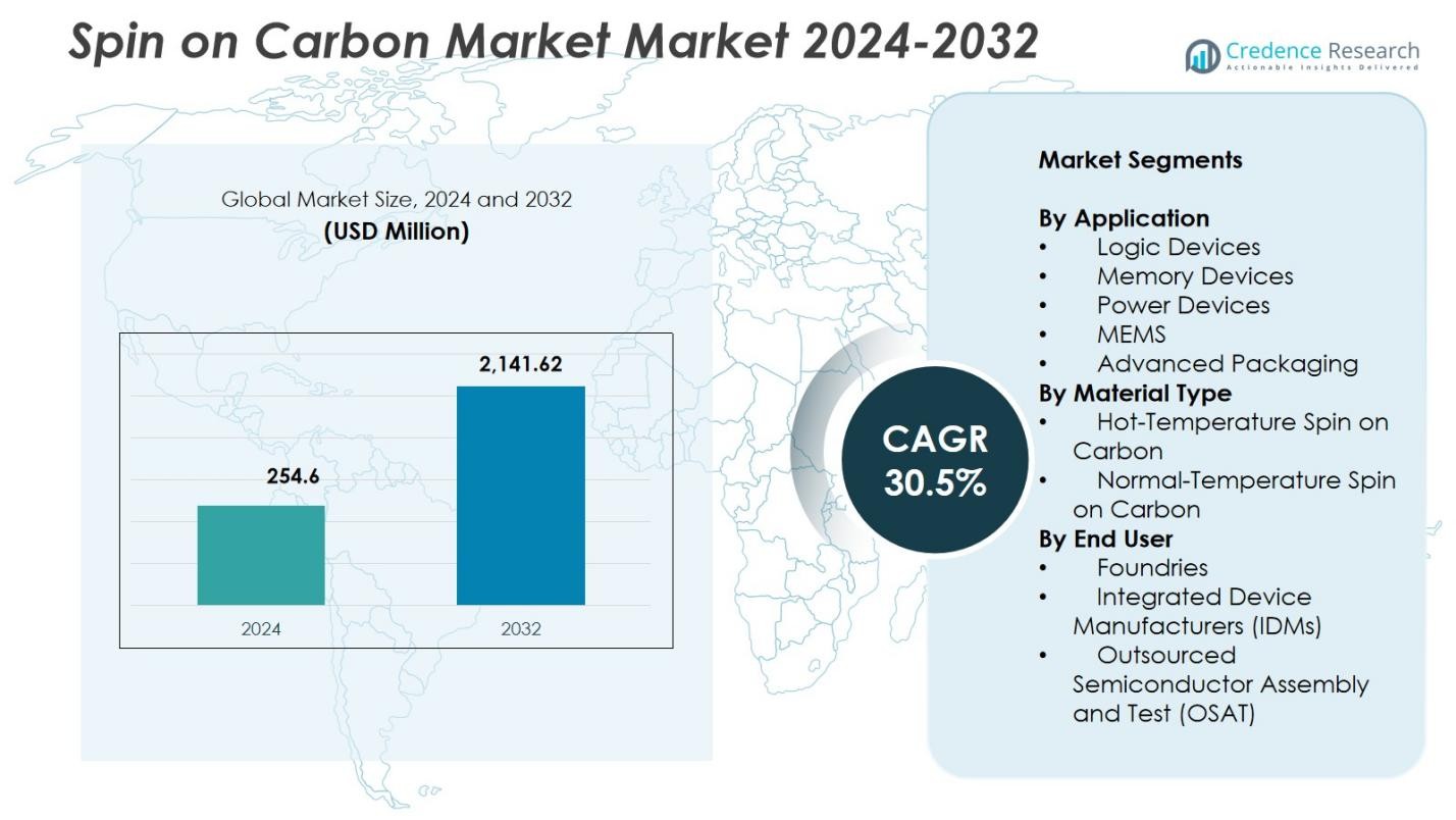
Spin on Carbon Market size was valued at USD 254.6 Million in 2024 and is anticipated to reach USD 2,141.62 Million by 2032, at a CAGR of 30.5% during the forecast period.
| REPORT ATTRIBUTE |
DETAILS |
| Historical Period |
2020-2023 |
| Base Year |
2024 |
| Forecast Period |
2025-2032 |
| Spin on Carbon Market Size 2024 |
USD 254.6 Million |
| Spin on Carbon Market, CAGR |
30.5% |
| Spin on Carbon Market Size 2032 |
USD 2,141.62 Million |
Spin on Carbon Market features leading participants such as Samsung SDI Co., Ltd., Merck KGaA, Shin-Etsu Chemical Co., Ltd., YCCHEM Co., Ltd., Brewer Science, Inc., JSR Micro, Inc., KOYJ Co., Ltd., Irresistible Materials Ltd., Nano-C, Inc., and DNF Co., Ltd., who focus on advancing high-purity, thermally stable carbon formulations for next-generation semiconductor nodes. Asia-Pacific led the global Spin on Carbon Market in 2024 with a 38.7% share, supported by extensive foundry and IDM activity in Taiwan, South Korea, China, and Japan. North America and Europe followed, driven by strong investments in advanced lithography, logic devices, and memory manufacturing.
Access crucial information at unmatched prices!
Request your sample report today & start making informed decisions powered by Credence Research Inc.!
Download Sample
Market Insights
- Spin on Carbon Market reached USD 254.6 Million in 2024 and is projected to grow at a CAGR of 30.5% through 2032.
- Market growth is driven by rising adoption of EUV lithography and advanced patterning, with logic devices holding a 38.4% share due to rapid scaling of sub-5 nm technologies.
- Key trends include increasing use of spin-on carbon in GAA transistor fabrication and expanding demand for high-temperature formulations in deep-etch semiconductor processes.
- Major players focus on developing high-purity, thermally stable materials, strengthening their presence across advanced logic, memory, and packaging applications while addressing integration challenges and process sensitivity.
- Asia-Pacific led the global market with a 38.7% share in 2024, followed by North America and Europe, supported by extensive fab expansions and strong semiconductor manufacturing capabilities.
Market Segmentation Analysis:
By Application:
In the Spin on Carbon Market, logic devices dominated the application segment with a 38.4% share in 2024, driven by the rapid scaling of advanced nodes and increased adoption of EUV lithography. Spin-on carbon materials provide exceptional etch resistance and uniformity required for multi-patterning, supporting gate-all-around (GAA) architectures and high-density interconnects. Memory devices accounted for rising usage as 3D NAND and DRAM manufacturers seek reliable hardmask solutions for deep etching. Power devices, MEMS, and advanced packaging also contributed to demand as semiconductor producers emphasize process precision, cost efficiency, and integration complexity reduction.
- For instance, Brewer Science’s OptiStack SOC450 spin-on carbon platform, launched in June 2023, targets logic and 3D architectures by providing zero shrinkage up to 550 °C, strong gap-fill, and improved pattern collapse resistance for advanced-node lithography.
By Material Type:
Hot-temperature spin-on carbon led the material type segment with a 56.7% share in 2024, owing to its superior thermal stability, high carbon content, and suitability for demanding etch processes in sub-5 nm manufacturing. Its ability to withstand aggressive plasma conditions makes it essential for high-aspect-ratio patterning steps in advanced logic and memory production. Normal-temperature spin-on carbon maintained steady adoption in less complex patterning layers where cost efficiency and process simplicity are prioritized. Growth across both materials is supported by increasing device miniaturization and expanding EUV-enabled manufacturing.
- For instance, Merck KGaA’s AZ spin-on carbon products offer high thermal stability for diverse integration flows and superior throughput versus CVD alternatives. These materials ensure high transparency for overlay control in semiconductor patterning applications.
By End User:
Foundries commanded the largest end-user share at 47.2% in 2024, driven by accelerated investments in advanced node manufacturing at 5 nm, 3 nm, and emerging 2 nm processes. Their continuous demand for reliable hardmask materials strengthens the adoption of spin-on carbon in multi-patterning and GAA transistor fabrication. Integrated Device Manufacturers (IDMs) contributed significantly as they scale both logic and memory production, while OSATs expanded usage in advanced packaging flows requiring precise pattern transfer. Rising semiconductor outsourcing and expanding fab capacity further enhance end-user adoption.
Key Growth Drivers
Increasing Adoption of EUV Lithography and Advanced Patterning
The Spin on Carbon Market expands rapidly as semiconductor manufacturers intensify the adoption of EUV lithography and advanced patterning technologies required for sub-5 nm logic and next-generation memory devices. Spin-on carbon provides high etch selectivity, dimensional stability, and uniform film coverage essential for multi-patterning steps in GAA transistors and 3D NAND architectures. Its ability to withstand aggressive plasma conditions and support high-aspect-ratio structures strengthens its role as a foundational material in advanced semiconductor fabrication.
- For instance, Samsung SDI supplies spin-on carbon materials that are integral to advanced patterning processes in their 3nm and 2nm gate-all-around (GAA) transistor production, supporting the uniform film coverage and etch selectivity needed for stacked nanosheet architectures.
Rapid Expansion of Foundry and IDM Capacity
Growing global investments in semiconductor fabrication capacity significantly drive the market for spin-on carbon. Leading foundries and IDMs—including TSMC, Samsung, Intel, and major memory manufacturers—are scaling 5 nm, 3 nm, and emerging 2 nm technologies, increasing demand for thermally stable and precise hardmask materials. Rising chip consumption across AI, automotive, HPC, and consumer electronics, combined with regional initiatives for semiconductor self-sufficiency, reinforces large-scale adoption of spin-on carbon across advanced process workflows.
- For instance, Intel facilities in the U.S., such as those in Arizona, adopted spin-on carbon materials to support sub-7nm and 3D chip architectures, optimizing lithography and dielectric steps for enhanced device performance.
Growth of Advanced Packaging and 3D Integration
The rapid transition toward advanced packaging architectures—such as 2.5D/3D stacking, chiplets, hybrid bonding, and wafer-level packaging—creates strong demand for spin-on carbon solutions. These materials deliver reliable pattern transfer, excellent gap-filling capability, and stable performance under high-temperature processes required in RDL formation, TSV etching, and micro-bump patterning. As heterogeneous integration becomes central to next-generation semiconductor design, spin-on carbon’s versatility strengthens its importance across advanced packaging and interconnect applications.
Key Trends & Opportunities
Rising Use in GAA and Vertically Scaled Semiconductor Architectures
A major trend reshaping the Spin on Carbon Market is the accelerated adoption of gate-all-around (GAA) transistors and vertically scaled memory devices. These architectures demand precise patterning, deep-etch uniformity, and reliable hardmask performance that spin-on carbon materials deliver. Their stability and narrow linewidth control make them indispensable for nanosheet and nanowire transistor fabrication. As manufacturers push beyond traditional lithographic limitations, high-temperature and next-generation carbon formulations represent a substantial long-term opportunity.
- For instance, Merck KGaA offers spin-on carbon materials with high thermal stability and transparency for overlay control, aiding reliable hardmask performance in vertically scaled memory device integration flows.
Advancements in Low-Defect and Chemically Tunable Material Formulations
The market experiences a strong opportunity from the development of low-defect, tunable spin-on carbon materials engineered to improve yield and process reliability in advanced semiconductor nodes. Suppliers increasingly offer formulations with adjustable viscosity, enhanced density, and improved compatibility with multi-patterning stacks. These advancements enable fabs to optimize patterning performance, reduce defect-related rework, and achieve better uniformity. As device architectures grow more complex, demand for customizable, high-performance carbon materials continues to expand.
- For instance, Merck KGaA’s AZ® spin-on carbon (SoC) products deliver high transparency to enhance overlay control and high thermal stability for integration in multi-patterning flows.
Key Challenges
High Process Sensitivity and Complex Integration Requirements
A significant challenge in the Spin on Carbon Market is managing the material’s sensitivity within advanced lithography and etching workflows. Achieving consistent performance requires rigorous control over film uniformity, thickness stability, thermal behavior, and defect minimization. Even minor process deviations during coating, baking, or etching can alter critical dimensions and impact yield. As semiconductor nodes shrink further, fabs must invest heavily in process optimization and material qualification to ensure smooth integration.
Competition from Alternative Hardmask and Etch-Resistant Materials
Spin-on carbon faces strong competitive pressure from other hardmask options, including amorphous carbon films (a-C), silicon-based hardmasks, and hybrid organic–inorganic materials. These alternatives may offer advantages in specific etch stacks or integration flows, prompting fabs to evaluate multiple solutions to balance cost, performance, and compatibility. This competitive landscape requires continuous innovation, improved material engineering, and stronger value differentiation from spin-on carbon suppliers to maintain adoption in emerging semiconductor technologies.
Regional Analysis
North America
North America held a 31.6% share in the Spin on Carbon Market in 2024, driven by strong semiconductor manufacturing activity, particularly in advanced logic and AI-oriented chip production. Extensive investments in new fabrication facilities, supported by government initiatives such as the U.S. CHIPS Act, continue to elevate demand for advanced patterning materials like spin-on carbon. The region benefits from leading IDM and foundry expansions, robust R&D capabilities, and a growing focus on reshoring critical semiconductor supply chains. Rising adoption of EUV-based nodes further strengthens the material’s relevance across major U.S. chip manufacturing hubs.
Europe
Europe accounted for a 22.4% share of the Spin on Carbon Market in 2024, supported by the region’s expanding semiconductor ecosystem and strategic emphasis on technological sovereignty. Key countries such as Germany, France, and the Netherlands invest heavily in advanced lithography, metrology, and patterning technologies. The presence of leading equipment manufacturers and collaborative R&D initiatives in nanofabrication drive material innovation and adoption. Europe’s increasing focus on automotive electronics, industrial automation, and green technology accelerates semiconductor demand, reinforcing the integration of spin-on carbon in advanced logic, memory, and power device manufacturing.
Asia-Pacific
Asia-Pacific dominated the global market with a 38.7% share in 2024, underpinned by its leadership in semiconductor fabrication and high-volume manufacturing. Countries including Taiwan, South Korea, China, and Japan host top-tier foundries and IDMs that aggressively scale sub-7 nm and 3 nm production. Massive investments in EUV lithography, 3D NAND, and advanced packaging propel demand for high-performance spin-on carbon materials. The region’s strong electronics supply chain, rising consumption of consumer and industrial electronics, and continuous fab expansions position Asia-Pacific as the fastest-growing market for next-generation carbon hardmask solutions.
Middle East & Africa
The Middle East & Africa represented a 3.2% share of the Spin on Carbon Market in 2024, with growth supported by emerging investments in semiconductor design, electronics manufacturing, and technology-focused economic diversification programs. Countries such as the UAE and Saudi Arabia increasingly develop innovation ecosystems targeting advanced electronics and AI applications. Although the region lacks large-scale fabrication facilities, growing partnerships with global semiconductor players and rising demand for consumer electronics support incremental adoption. Government-backed digital transformation strategies further encourage the integration of modern materials and technologies, including spin-on carbon, within niche manufacturing segments.
South America
South America captured a 4.1% share of the Spin on Carbon Market in 2024, driven by expanding demand for consumer electronics, telecommunications infrastructure, and industrial automation components. Brazil and Argentina lead regional semiconductor activity, focusing primarily on assembly, testing, and localized chip packaging. While large-scale semiconductor fabrication remains limited, increasing investments in microelectronics R&D and partnerships with international manufacturers create opportunities for specialized materials such as spin-on carbon. Market growth is supported by rising digitalization, growing adoption of advanced devices, and government initiatives aimed at strengthening technological capabilities across the region.
Market Segmentations:
By Application
- Logic Devices
- Memory Devices
- Power Devices
- MEMS
- Advanced Packaging
By Material Type
- Hot-Temperature Spin on Carbon
- Normal-Temperature Spin on Carbon
By End User
- Foundries
- Integrated Device Manufacturers (IDMs)
- Outsourced Semiconductor Assembly and Test (OSAT)
By Geography
- North America
- Europe
- Germany
- France
- U.K.
- Italy
- Spain
- Rest of Europe
- Asia Pacific
- China
- Japan
- India
- South Korea
- South-east Asia
- Rest of Asia Pacific
- Latin America
- Brazil
- Argentina
- Rest of Latin America
- Middle East & Africa
- GCC Countries
- South Africa
- Rest of the Middle East and Africa
Competitive Landscape
Competitive landscape in the Spin on Carbon Market features key players including Samsung SDI Co., Ltd., Merck KGaA, Shin-Etsu Chemical Co., Ltd., YCCHEM Co., Ltd., Brewer Science, Inc., JSR Micro, Inc., KOYJ Co., Ltd., Irresistible Materials Ltd., Nano-C, Inc., and DNF Co., Ltd. The market remains innovation-driven, with companies focusing on high-purity formulations, enhanced thermal stability, and improved etch resistance to meet the requirements of EUV lithography, multi-patterning, and advanced logic and memory manufacturing. Leading suppliers invest heavily in R&D to develop next-generation high-temperature spin-on carbon materials tailored for sub-5 nm nodes and GAA transistor structures. Strategic collaborations between material manufacturers, foundries, and equipment suppliers further strengthen product integration and process compatibility. Companies also expand production capacities and optimize supply chains to meet rising demand from advanced semiconductor fabrication hubs in Asia-Pacific, North America, and Europe, maintaining a strong competitive edge in this fast-evolving market.
Shape Your Report to Specific Countries or Regions & Enjoy 30% Off!
Key Player Analysis
- Irresistible Materials Ltd. (U.K.)
- Brewer Science, Inc. (U.S.)
- DNF Co., Ltd. (South Korea
- Merck KGaA, Darmstadt (Germany)
- JSR Micro, Inc. (U.S.)
- KOYJ Co., Ltd. (South Korea)
- Nano-C, Inc. (U.S.)
- Samsung SDI Co., Ltd. (South Korea)
- Shin-Etsu Chemical Co., Ltd. (Japan)
- YCCHEM Co., Ltd. (South Korea)
Recent Developments
- In November 2025, Hengkun New Materials (China) announced that its in-house SOC (spin-on carbon) products have reached mass production, including SOC hardmask materials, alongside other lithography materials like BARC and KrF/i-Line photoresists marking a significant commercial scale milestone for the company’s SOC product line.
- In June 2025, Merck KGaA continued to build on its earlier acquisition of Versum Materials by integrating and promoting its expanded spin-on carbon hardmask portfolio for next‑generation semiconductor manufacturing, positioning the combined business as a key materials supplier for advanced logic and memory nodes.
Report Coverage
The research report offers an in-depth analysis based on Application, Material Type, End User and Geography. It details leading market players, providing an overview of their business, product offerings, investments, revenue streams, and key applications. Additionally, the report includes insights into the competitive environment, SWOT analysis, current market trends, as well as the primary drivers and constraints. Furthermore, it discusses various factors that have driven market expansion in recent years. The report also explores market dynamics, regulatory scenarios, and technological advancements that are shaping the industry. It assesses the impact of external factors and global economic changes on market growth. Lastly, it provides strategic recommendations for new entrants and established companies to navigate the complexities of the market.
Future Outlook
- The market will experience strong growth as EUV lithography adoption expands across advanced semiconductor nodes.
- Spin-on carbon materials will gain wider use in supporting GAA transistor fabrication and nanosheet integration.
- High-temperature carbon formulations will become increasingly important for deep-etch applications in logic and memory devices.
- Foundries and IDMs will drive sustained demand through continuous capacity expansion and node scaling.
- Advanced packaging technologies, including hybrid bonding and 3D stacking, will strengthen the need for precise carbon hardmask materials.
- R&D efforts will focus on reducing defect density and improving film uniformity for next-generation patterning.
- Collaboration between material suppliers and equipment manufacturers will accelerate process optimization.
- The market will see rising adoption in Asia-Pacific as semiconductor manufacturing continues to dominate the region.
- New eco-engineered and chemically tunable carbon formulations will emerge to enhance process flexibility.
- Competitive pressure will encourage suppliers to innovate high-performance solutions for sub-3 nm semiconductor technologies.


